Note: Descriptions are shown in the official language in which they were submitted.
WO 2022/192990
PCT/CA2022/050352
AN INCOHERENT CLOCKING METHOD
TECHNICAL FIELD OF THE INVENTION
[0001] The present invention relates to a clock and timing solution for an
antenna of a
radio telescope antenna array.
BACKGROUND OF THE INVENTION
[0002] The timing of radio telescope arrays is vital to its operation. Current
methods of
timing delivery to each antenna of a radio telescope array include passive
clock
distribution via stabilized media, moving the analogue RE signal from each
element to a
central location via coax or fiber to compact the area over which clock
distribution must
occur and therefore simplify it, or active round-trip phase-corrected clock
"steering"
using specialized photon ics methods. Each of these methods has its advantages
and
limitations, in terms of distance over which the clock can be distributed,
clock frequency,
and signal fidelity. The method of "incoherent clocking" as disclosed in
Carlson, B.R.,
"Incoherent clocking in coherent radio interferometers," IEE Electronics
Letters 54(14),
909-911(2018) aims to provide a cost-effective, all-digital clock and timing
solution for
any cost, scale, and frequency of radio telescope. With incoherent clocking,
rather than
distribute a common clock to all elements, each antenna performs down-
conversion and
digitization using its own free-running independent local oscillator (LO),
measuring its
frequency sufficiently accurately in a reference/common clock domain, and then
digitally
re-sampling (i.e. interpolating) the data accordingly prior to final
operations such as
correlation and beamforming. All of these operations, including measuring and
compensating for element-to-central media instabilities, are performed using
all-digital
methods in readily available digital devices such as Field Programmable Gate
Arrays
(FPGAs), using Commercial Off-The-Shelf (COTS) digital fiber optic modules,
and the
most inexpensive fiber routing there is, namely aerial fiber using digital
communications-
grade cable (e.g. "loose-tube" without special vibration dampening gel), for
element-to-
central communications. All serial communications occurring over fiber, and
the
operation of IC itself, is within industry-established SERDES
(SERializer/DESerializer)
jitter masks ¨ there is no specialized tuning or operation outside COTS
specifications.
1
CA 03212306 2023- 9- 15
WO 2022/192990
PCT/CA2022/050352
[0003] A simplified block diagram of the incoherent clocking method is shown
in Figure
1. In this diagram each antenna performs down-conversion (if required, not
shown) and
digitization using its own antenna LO (aL0) and its timing is transferred,
intrinsically with
the clocking of digitized data into a serial stream, to the central site via
full-duplex/bi-
directional fiber link. In Figure 1, an example antenna 10 is shown of a radio
telescope
antenna array (not shown). The antenna 10 is located remotely from a central
site 20 of
the radio telescope antenna array. The antenna 10 receives an analog radio
frequency
(RE) signal 11 containing science data. In particular, the RE signal 11 is
input into an
analog to digital converter (ADC) 12. Clocking of the ADC 12 is provided by
aL0 13.
The converted digital data 14 that is output from ADC 12 is input into a
digital serial
transceiver 15. The digitized data that is output from digital serial
transceiver 15 is
transmitted as a serial stream to the central site 20 via a full-duplex fiber
link 30. As
shown, the timing of the aL0 13 is transferred intrinsically with the clocking
of the
digitized serial stream to the central site 20. At the central site 20, a
digital serial
transceiver 21 receives the digitized serial data stream transmitted over the
fiber link 30.
The timing of the aL0 13 clock is recovered from the processing of the
digitized serial
data stream in digital serial transceiver 21 and is input into block 22 along
with the
digitized data. In block 22, the digitized data is "corrected" from clocking
in the aL0 13
domain to the domain of a common central LO clock 23 of the central site 20.
The fibre
link delay of the fibre link 30 is continuously measured by the central site
20 via a round-
trip phase measurement (not shown). This measurement is included in the
"corrections"
to the digitized data received from the remote antenna 10. The digitized data
output
from block 22 is then "corrected" to the common clock 23 of the central site
20 and can
then be used for further operations such as correlation and beamforming.
[0004] One of the drawbacks with Carlson, B.R., "Incoherent clocking in
coherent radio
interferometers," IEE Electronics Letters 54(14), 909-911 (2018) may include
beating
effects due to sampling of the digital discrete-time waveform derived from the
serial
receiver 21 with the sampling frequency derived from the central LO 23. If the
frequency of the waveform is harmonically related to the sampling frequency
derived
from the central LO, then there will be indeterminate periods of time when the
discrete-
time waveform is repetitively sampled at particular phase epochs¨when the
phase of
2
CA 03212306 2023- 9- 15
WO 2022/192990
PCT/CA2022/050352
the waveform naturally drifts, at some point a discrete phase jump happens in
the
sampled phase, introducing a discontinuity in the sampled waveform to be
measured.
This effect can be entirely mitigated by ensuring that the discrete-time
waveform is at a
frequency such that it is always repetitively sampled at different phases so
that no such
phase discontinuity in the sampled waveform ever occurs.
SUMMARY OF THE INVENTION
[0005] The present invention aims to overcome the problem of beating effects
described
above.
[0006] According to an aspect of the present invention, there is provided a
method of
sampling, at a central site of a radio telescope array, a signal at a second
clock
frequency from a remote antenna when the signal is at a first clock frequency,
the
method comprising:
a. receiving the signal from a remote antenna;
b. converting the signal into a first binary format;
c. writing the signal into successive first addresses of a dual-port memory at
each clock cycle of the first clock frequency, wherein the first addresses
are generated by an address counter in the first binary format;
d. converting the first addresses in the first binary format from the address
counter into intermediate addresses in a second binary format;
e. writing the intermediate addresses in the second binary format into at
least
one register at each clock cycle of the second clock frequency, wherein
the second clock frequency is larger than the first clock frequency;
f. converting the intermediate addresses, from the at least one register, from
the second binary format into the first binary format to generate
successive read addresses; and
g. reading the signal from the dual-port memory at the generated read
addresses at each clock cycle of a multiple of the second clock frequency.
[0007] In some embodiments of the present invention, there is provided the
method as
described herein, wherein the second binary format is Gray code.
3
CA 03212306 2023- 9- 15
WO 2022/192990
PCT/CA2022/050352
[0008] In some embodiments of the present invention, there is provided the
method as
described herein, wherein the at least on register comprises a shift register.
[0009] In some embodiments of the present invention, there is provided the
method as
described herein, wherein the at least on register comprises a decimation
register.
[0010] In some embodiments of the present invention, there is provided the
method as
described herein, wherein the at least on register comprises a shift register.
[0011] In some embodiments of the present invention, there is provided the
method as
described herein, wherein the multiple of the second clock frequency comprises
0.25.
[0012] In some embodiments of the present invention, there is provided the
method as
described herein, wherein:
a. a round-trip tracer phase is measured;
b. the round-trip-measured tracer phase is transmitted to the central site;
c. the round-trip-measured tracer phase is used as a compensating factor into
the
central-site frequency tracker;
d. the central-site frequency tracker measures the tracer frequency;
e. the tracer frequency from the frequency tracker is filtered with a digital
low-pass
filter to remove confusing effects;
f. the low-pass filtered tracer frequency is used to re-sample and phase-
correct the
digitized science data; and
g. the digitized science data may be delayed by the same amount as the delay
of
the frequency tracker and low-pass filter to ensure that the measured and
filtered
tracer frequency is applied to the digitized science data at the time when the
digitized science data was down-converted and digitized at frequencies
directly
proportional to the applied tracer frequency measurement.
[0013] According to another aspect of the present invention, there is provided
a
system at a central site of a radio telescope array for sampling a signal at a
second
clock frequency from a remote antenna when the signal is at a first clock
frequency,
the system comprising:
4
CA 03212306 2023- 9- 15
WO 2022/192990
PCT/CA2022/050352
a. a transceiver that receives the signal from a remote antenna;
b. a first converter for converting the signal into a first binary format;
c. an address counter for generating successive first addresses in the first
binary format;
d. a dual-port memory that stores the signal at the successive first addresses
at each cycle of the first clock frequency;
e. a second converter for converting the first addresses in the binary format
from the address counter into intermediate addresses in a second binary
format;
f. at least one register that stores the intermediate addresses in the second
binary format at each clock cycle of the second clock frequency, wherein
the second clock frequency is larger than the first clock frequency; and
g. a third converter that converts the intermediate addresses from the at
least one register from the second binary format into the fist binary format
to generate successive read addresses,
wherein the signal from the dual-port memory is read from the dual-port memory
at the
generated ready addresses at each clock cycle of a multiple of the second
clock
frequency.
BRIEF DESCRIPTION OF THE DRAWINGS
[0014] Figure 1 shown a simplified block diagram of the incoherent clocking
method.
[0015] Figure 2 shows a more detailed implementation of the incoherent
clocking
method as shown in Figure 1.
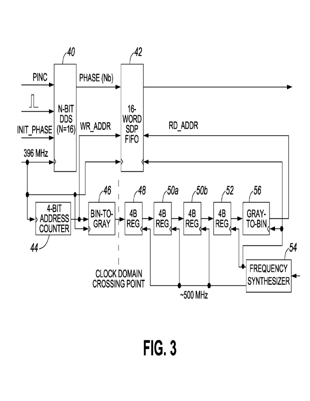
[0016] Figure 3 shows a phase generator/sampler at the central site.
DETAILED DESCRIPTION
[0017] Figure 2 shows a detailed implementation of Figure 1, which is a
typical
implementation, but not the only one. An antenna 10 is shown that is remote
from a
central site 20 of a radio telescope antenna array. The antenna 10 receives
data in form
of an RF signal 7. RF signal 7 is amplified by amplifier 8 and down conversion
9 is
CA 03212306 2023- 9- 15
WO 2022/192990
PCT/CA2022/050352
performed, if required, using the clock of the antenna LO (aL0) 13. The RF
signal 11 is
then input into ADC 12. Clocking of the ADC 12 is based on the aL0 13. The
digitized
science data 14 is then input into digital serial transceiver 15 which can be
implemented
by a field-programmable gate array (FPGA).
[0018] The digitized science data and incoherent clocking signaling from a
round-trip
phase detector 16 are merged together by multiplexer 17 into
serializer/deserializer
(SERDES) 18. SERDES 18 converts the digitized science data into a serial
stream for
transmission over the full duplex/bidirectional fiber link 30. The digitized
serial stream is
processed at the central site 20 but also looped-back to the remote antenna
10. This
loopback must retain timing information contained in the received digitized
serial
stream, although it can filter out jitter occurring on timescales faster than
aL0 frequency
variations that need to be measured and corrected.
[0019] The incoherent clocking signaling comprises "tracer" signaling, which
contains a
pulse for a round-trip delay measurement, the streaming round-trip measured
tracer
phase, and¨on the pulse¨the current tracer phase at each tracer DDS 40. The
term
"tracer" is a term used in incoherent clocking to refer to a high signal-to-
noise ratio
(SNR) complex digital tone which is typically around 10 MHz. This tone is
developed for
local use in various places by a Direct Digital Synthesizer (DDS) (not shown)
driven by
various clocks such as the SERDES CDR PLL-recovered clock. There is a fixed a
priori
established ratio, in any IC design, of the heterodyne down-conversion LO and
ADC
clock frequencies to the tracer frequency. Additionally, the tracer phase is
transferred
across digital clock domains using Gray-code methods so that phase coding
errors do
not occur, and intelligent choice of the tracer frequency prevents any beating
effects
that might occur, for instance if the aL0 frequency is, for a short period of
time, very
close to the reference clock frequency.
[0020] Returning to Figure 2, when transmitting the digitized serial stream, a
first DDS
(not shown) in the round-trip phase detector 16 is driven by aLO. When looped-
back, a
second DDS (not shown) in 16 is driven by the signal RX_CDR_CLK, which is a
clock
signal synchronous with the received data. The phase of this data-recovered
clock is
perturbed by fiber delay variations, which in turn perturbs the tracer phase
by a
6
CA 03212306 2023- 9- 15
WO 2022/192990
PCT/CA2022/050352
proportional amount. The round-trip phase detector in 16 continuously measures
the
phase of the tracer loopback return side relative to the transmit side,
divided by 2, and
sent as a continuous stream of phase measurements, typically every 10ps to the
central
site 20. The measurement is "round-trip" so it therefore measures the
contribution of
both directions of fiber, but as only one direction of the compensation is
desired, the
round-trip measurement is divided by 2. These measurements form part of the
incoherent clocking signaling that is merged with the digital science data by
multiplexer
17 before being transmitted to the central site 20.
[0021] At the central site 20, SERDES 24 at the central site 20 recovers the
digitized
science data from the digitized serial stream received over the fiber link 30.
SERDES 24
also extracts the signal RX_CDR_CLK as well as the incoherent clocking
signaling. As
described above, the incoherent clocking signaling comprises tracer signaling,
including
the streaming round-trip measured tracer phase. A demultiplexer 25
demultiplexes the
data signal output from SERDES 24 into the digitized science data and the
incoherent
clocking signaling.
[0022] An aL0 digital frequency tracker 26 at the central site 20 uses the
round-trip-
measured phase measurements from the incoherent clocking signaling as
compensating input to remove effects of fiber delay perturbations on
timescales that are
confused with aL0 frequency variations. Faster variations that cannot be
relied on due
to the length of the fiber link 30 are ultimately filtered out by the low pass
filter (LPF)
finite impulse response (FIR) filter 27. The signal RX_CDR_CLK also drives a
local
tracer DDS (not shown) in the aL0 digital frequency tracker 26 in the central
site 20.
The digitized science data is written into the digital re-sampler and mixer
28. The tracer
signaling and round trip-calculated streaming tracer phase measurements are
used by
antenna LO digital frequency tracker 26 to sufficiently and precisely measure
the local
tracer output frequency of the DDS located therein. This measurement of the
local
tracer output frequency of the DDS, after the LPF 27, must be at a sufficient
level of
accuracy and precision for correcting the digitized science data. Since there
is a delay
through the LPF 27 that can be quite large, memory in the Re-Sampler 28 can be
sized
to match it, ensuring that the frequency measurement out of the LPF is applied
at the
7
CA 03212306 2023- 9- 15
WO 2022/192990
PCT/CA2022/050352
correct time. This is a major advantage of the incoherent clocking technique
over other
round-trip clock steering approaches. Measured frequency variations can be
applied to
the data at the time when they happened rather than, effectively, some lag
time later.
[0023] The filtered tracer frequency measurements, f tracer(t), are multiplied-
up to the
antenna ADC frequency and, if equipped, the heterodyne mixer 9 frequency, and
drive
the digital re-sampler and mixer 28. The output of the digital re-sampler and
mixer 28
represents the final "corrected" output in the common clock 23 of the central
site 20.
[0024] As described above, both the phase detector 16 and the aL0 digital
frequency
tracker 26 make use of tracer signaling and the round-trip measured phase. In
both the
phase detector 16 and the aL0 digital frequency tracker 26, it is necessary to
sample
the tracer phase to a common clock domain, either to the clock domain of the
aL0 10 or
the clock domain of the central site 20. To do this, the tracer phase is
transferred across
digital clock domains using Gray-code and dual-port memory methods. The
inventor
has discovered that using these methods allows for any arbitrary tracer
frequency to be
used; with proper choice of tracer frequency any beating effects are entirely
removed.
[0025] The use of Gray-code and dual-port methods is described in more detail
in
Figure 3. The pulse of the tracer signaling is input into a 16-bit DDS 40,
although any
number of bits can be used for the DDS, as well as the tracer phase present at
the
antenna at that same pulse epoch, thereby synchronizing tracer phases across
the fiber
link. This pulse and phase representing the tracer signaling is synchronous
with the
RX_CDR_CLK clock, for example 396 MHz, The 16-bit DDS is a structure
comprising a
phase increment ("pine) register and accumulator. Every 396 MHz clock cycle a
phase
increment, pinc, is added to the phase register to produce a sawtooth PHASE
waveform. The tracer frequency f .tracer is always related to the aL0 by the
following
equation:
pinc
ftracer = 2Nb_Das X fDDS
where faDs is the aLO-derived frequency of the clock used to clock the DDS,
and
Nb DDS is the number of bits in the DDS. In the present case, fDDs is 396
MHz.The
sawtooth waveform represents the tracer phase synchronous with the 396 MHz
clock.
8
CA 03212306 2023- 9- 15
WO 2022/192990
PCT/CA2022/050352
[0026] The output signal of the 16-bit DDS 40 is a 16-bit binary number
sampled at
396MHz. The next step is to sample the tracer phase into a clock domain of the
central
site 20 which is different from the remote antenna clock domain, present at
the central
site as the RX_CDR_CLK domain. Attempting to simply sample the 16-bit DDS
output
into a different clock domain will result in coding errors. On a sampling
clock edge, if the
setup and hold times of the input signal to a digital storage register are
incorrect, the
sampled output is indeterminate resulting in coding errors when more than 1
bit of a
word with an arbitrary bit pattern is sampled. Accordingly, the inventor
decided to use a
memory structure to store the tracer phase. In particular, the tracer phase is
written into
a memory structure such as a simple dual port first-in, first-out (FIFO)
buffer 42. The
FIFO buffer 42 has a write port with a corresponding independent write clock
and a read
port with a corresponding independent read clock. The FIFO buffer 42 comprises
random-access memory (RAM). At each clock cycle of the 396MHz reference clock,
the
output of the 16-bit DDS 40 representing the tracer phase is written into the
FIFO buffer
42. The invention is not limited to a 16-bit DDS. A DDS of any number of bits
can be
used. A 4-bit address counter 44 provides the write addresses for the FIFO
buffer 42.
When the tracer phase is read out from FIFO buffer 42, the reference clock of
the
central site 20 is used. The tracer phase is written into the FIFO buffer 42
without error.
[0027] To ensure that the tracer phase is accurately read out, it is important
that coding
errors are avoided. An established method of ensuring there are no coding
errors
across digital clock domain crossings is to use Gray code. Gray code is an
ordering of
the binary numeral system where two successive values differ in only one bit.
As only
one bit is being changed the chance of sampled code errors is eliminated
compared to
binary numeral system where multiple bits can change between successive
values,
provided the sampling clock frequency is sufficiently higher than the source
clock
frequency. The conversion from binary to Gray code is done by binary-to Gray
code
converter 46 which uses a well-known algorithm to convert the output of the 4-
bit
address counter 44 into Gray code. It is known that Gray code will only work
if there are
2n states where n is the number of bits. As the input to the binary-to-Gray
code
converter 46 is 4 bits, there will be 16 states. It is also possible to
combine the functions
of the 4-bit address counter 44 and the binary-to-Gray code converter 46 by
simply
9
CA 03212306 2023- 9- 15
WO 2022/192990
PCT/CA2022/050352
using a Gray-code counter. The output of the binary-to-Gray code converter 46
is input
into a 4-bit register 48. It is here that the clock domain crosses over from
the 396MHz
domain into the clock domain of the central site 20. The clock domain of the
central site
20 should be sufficiently larger than the originating clock domain to ensure
that no state
is missed which would result in Gray-code errors when the clock domain crosses
over
from one clock domain to the next. It is important that no state is missed.
The inventor
realized that a clock domain of -500 MHz would work, although any appropriate
frequencies for both can be used. Every 396 MHz, the output of the binary-to-
Gray
converter 46 changes by one bit. This one bit change every 396 MHz is put into
4-bit
register 48, but register 48 is clocked at 500 MHz.
[0028] From the 4-bit register 48, the Gray code passes into metastability
resolution
registers 50a and 50b. To ensure reliable operation, the input to a register
must be
stable for a minimum time before the clock edge (setup time) and for a minimum
time
after the clock edge (hold time). The register output is then available after
a specified
clock-to-output delay. If a data signal transition violates a register's setup
or hold time
requirements, the output of the register may go into a metastable state. In a
metastable
state, the register output hovers at a value between high and low states for
some period
of time inversely proportional to the register's speed, which means the output
transition
to a defined high or low state is delayed beyond the specified clock-to-output
delay. To
minimize the failures due to metastability in clock domain crossovers, a
sequence of
registers in the 500 MHz clock domain is used to resynchronize the Gray code
signal to
the new 500 MHz clock domain. The Gray code signal being output from the
metastability resolution registers 50a and 50b is now correctly being sampled
at the new
500 MHz clock domain. While subsequent processes can continue to be sampled at
500 MHz clock domain, it is more challenging to meet timing requirements in
digital
logic at this speed. Accordingly, to simplify timing, a 500 MHz/4 =125 MHz
clock can be
used for decimation register 52, and all subsequent processing of the sampled
tracer
phase. The FIFO and Gray code ensure there are no sampled tracer phase code
errors.
Once the tracer phase is sampled, it is possible to just use and process every
Nth
phase sample (i.e. decimate), provided that Nyquist zone-1 sampling of the
tracer
phase is satisfied. This allows the following logic to run at a lower speed.
CA 03212306 2023- 9- 15
WO 2022/192990
PCT/CA2022/050352
[0029] The 500 MHz and 125 MHz clocks can be supplied by a frequency
synthesizer
54, for example. The 125 MHz is not a requirement of the invention, but rather
an
embodiment of the invention that simplifies the digital logic timing. The
output of
decimation register 52 is then input into a Gray code-to-binary converter 56
and a binary
read address is output. This read address is inherently delayed by binary-to-
Gray
converter 46, registers 48, 50a, 50b and 52 and Gray-to-binary converter 56,
so it lags
the write address, to avoid RAM write/read memory access contention. However,
this
lag can't be more than the 4-bit repeat sequence¨if so, then 4 bits can be
increased to,
for example, 5 bits; similarly, 4 bits can be decreased to, for example, 3
bits if the lag
from binary-to-Gray converter 46, registers 48, 50a, 50b and 52, and Gray-to-
binary
converter 56 is small enough. This binary address is used as a read address
for the
FIFO buffer 42 to select the phase at this given read address. The phase is
then read
out at a clock frequency at each clock cycle of a multiple of the 500 MHz
clock, for
example 125 MHz. The phase output is now sampled at a multiple of the central
clock.
This phase output is then sent on for further processing.
[0030] The combination of the FIFO 42 and Gray-code phase sampling 44-56
allows for
any arbitrary pinc to be chosen; with appropriate choice, beating effects
previously
mentioned, can be entirely avoided.
11
CA 03212306 2023- 9- 15