Note: Descriptions are shown in the official language in which they were submitted.
WO 2022/213097
PCT/US2022/071453
Cavity Resonance Suppression Using Thermal Pedestal Arrangements
in Active Electronically Scanned Array
FIELD
100011 A low-cost easy to manufacture solution to address thermal, EMI
(Electro-Magnetic Interference), volume and location requirements for an
AESA (Active Electronically Scanned Array) is presented. The AESA includes
passive thermal pedestals interspersed in an arrangement with the AESA active
devices. The thermal pedestals are electrically and thermally conductive. The
AESA may be used in satellite communications and radar systems.
BACKGROUND
100021 The prior art uses a combination of thermal pedestals, EMI
gasketing material, and EMI ground tape to address the thermal, EMI, and
AESA active device placement requirements. The manufacture of the prior art
is relatively more expensive and has relatively more fabrication complexity.
Moreover, the reliability of the EMI ground tape is questionable.
SUMMARY
100031 This Summary is provided to introduce a selection of concepts in a
simplified form that is further described below in the Detailed Description.
This Summary is not intended to identify key features or essential features of
the claimed subject matter, nor is it intended to be used to limit the scope
of the
claimed subject matter.
100041 The present teachings provide a low-cost easy to manufacture
solution to address thermal, EMI (Electro-Magnetic Interference), volume and
location requirements for an AESA (Active Electronically Scanned Array). The
AESA thermal pedestals meet the EMI performance requirements by
suppressing cavity resonances of the AESA below a frequency greater than the
Rx and Tx frequency bands of the AESA. For example, when the upper limit of
the RX and TX frequency bands is 14.5 GHz, resonances below 15.5, 16.5, 17.5
1
CA 03212426 2023- 9- 15
WO 2022/213097
PCT/ITS2022/071453
or the like GHz are suppressed. The present teachings are applicable to RF
(Radio Frequency) communication systems, for example, RF communications
via LEO (Low Earth Orbit), ME0 (Medium Earth Orbit) or GEO
(Geosynchronous Earth Orbit) satellites and radar systems.
[0005] An AESA (Active Electronically Scanned Array), including: a
PCB (Printed Circuit Board) substrate having an obverse surface; TRMs
(Transmit/Receive Modules) disposed on the obverse surface; thermal pedestals
wherein each thermal pedestal includes a wall, having a wall height, including
wall surfaces and one of the wall surfaces being a contact surface; and a TIM
(Thermal Interface Material), having a TIM height, disposed between a
respective contact surface of the thermal pedestals and the obverse surface. A
plurality of the thermal pedestals are physically interconnected, the TIM is
electrically and thermally conductive, and the wall height plus the TIM height
is
sufficient to suppress resonances of the TRMs below a frequency greater than a
Tx and Rx frequency band of the TRMs.
[0006] The AESA may include a heat sink, wherein the thermal pedestals
extend from the heat sink.
[0007] The AESA may include fins extending from a first surface of the
heat sink, where the thermal pedestals extend from a second surface of the
heat
sink different than the first surface of the heat.
100081 The AESA where the heat sink, the fins and the thermal pedestals
are of a unitary, one-piece construction made, for example, from a metal
casting
process.
[0009] The AESA may include a ground layer disposed in the PCB and in
contact with the TIM.
[0010] The AESA where the arrangement of the thermal pedestals is
shaped as a waffle pattern.
[0011] The AESA where the thermal pedestals are organized with
substantial bilateral symmetry along both a first axis and a second axis
2
CA 03212426 2023- 9- 15
WO 2022/213097
PCT/ITS2022/071453
orthogonal to the first axis.
100121 The AESA where the TRMs are disposed in a non-equilateral
triangular lattice, an equilateral triangular lattice, a rectangular lattice,
or an
aperiodic lattice.
100131 The AESA may include antenna elements and a radome layer
disposed over a reverse surface of the PCB.
100141 The AESA may include a polarizer integrated with the radome.
100151 The AESA where the thermal pedestals, the TIM and the PCB
together form a stack having a cross-section depth less than or equal to 100
mils
(2.54 millimeter).
100161 The AESA where the thermal pedestals are of a unitary, one-piece
construction.
100171 The AESA where a thermal pedestal encircles, without contacting,
a respective one of the TRMs.
100181 The AESA where the interconnecting includes a web
interconnecting a plurality of the thermal pedestals.
100191 The AESA where the AESA is configured to operate in Ku and X
frequency bands.
100201 The AESA where the upper limit of the Tx and Rx frequency
bands is less than or equal to 14.5 GHz and the suppressed resonances are less
than equal to 16 GHz.
100211 The AESA is configured to operate with a scan angle 0 from 0 to
45 and a cp scan angle from 0 and 360 .
100221 The AESA is configured to operate with an upper end of the Tx
and Rx frequency bands less than or equal to 14.5 GHz with a scan angle 0 from
0 to 45 and a cp scan angle from 0 < < 360 .
100231 An AESA (Active Electronic Scanned Array) , including: a PCB
(Printed Circuit Board) substrate having an obverse surface; TRMs
(Transmit/Receive Modules) disposed on the obverse surface; thermal pedestals
3
CA 03212426 2023- 9- 15
WO 2022/213097
PCT/ITS2022/071453
wherein each thermal pedestal includes a wall, having a wall height, including
wall surfaces and one of the wall surfaces being a contact surface; a TIM
(Thermal Interface Material), having a TIM height, disposed between a
respective contact surface of the thermal pedestals and the obverse surface;
and
a heat sink including fins. In the AESA, a plurality of the thermal pedestals
are
physically interconnected, and the TIM is electrically and thermally
conductive,
the wall height plus the TIM height is sufficient to suppress resonances of
the
TRMs below a frequency greater than the Tx and Rx frequency bands of the
TRMs. In the AESA, the fins extend from a first surface of the heat sink and
the thermal pedestals extend from a second surface of the heat sink different
than the first surface of the heat. In the AESA, the heat sink, the fins and
the
thermal pedestals are of a unitary, one-piece construction, and the AESA is
configured to operate with an upper limit of the Tx and Rx frequency bands of
less than or equal to 14.5 GHz with a scan angle 0 from 0 to 450 and a y scan
angle from 00 < < 3600
.
10()241 Additional features will be set forth in the description that follows,
and in part will be apparent from the description, or may be learned by
practice
of what is described.
DRAWINGS
100251 In order to describe the manner in which the above-recited and
other advantages and features may be obtained, a more particular description
is
provided below and will be rendered by reference to specific embodiments
thereof which are illustrated in the appended drawings. Understanding that
these drawings depict only typical embodiments and are not, therefore, to be
limiting of its scope, implementations will be described and explained with
additional specificity and detail with the accompanying drawings.
100261 FIG. lA illustrates a top view of an exemplary thermal pedestal
according to various embodiments.
100271 FIG. 1B illustrates a cross-sectional view of an exemplary thermal
4
CA 03212426 2023- 9- 15
WO 2022/213097
PCT/ITS2022/071453
pedestal arrangement according to various embodiments.
100281 FIG. IC illustrates a top view of an exemplary thermal pedestal
arrangement.
100291 FIG. 2 illustrates a top view of a heat sink including thermal
pedestals according to various embodiments.
100301 FIG. 3 illustrates a cross-sectional view of an AESA according to
various embodiments.
100311 Throughout the drawings and the detailed description, unless
otherwise described, the same drawing reference numerals will be understood to
refer to the same elements, features, and structures. The relative size and
depiction of these elements may be exaggerated for clarity, illustration, and
convenience.
DETAILED DESCRIPTION
100321 Embodiments are discussed in detail below. While specific
implementations are discussed, this is done for illustration purposes only. A
person skilled in the relevant art will recognize that other components and
configurations may be used without parting from the spirit and scope of the
subject matter of this disclosure.
100331 The terminology used herein is for describing embodiments only
and is not intended to be limiting of the present disclosure. As used herein,
the
singular forms "a," "an" and "the" are intended to include the plural forms as
well, unless the context clearly indicates otherwise. Furthermore, the use of
the
terms "a," "an," etc. does not denote a limitation of quantity but rather
denotes
the presence of at least one of the referenced items. The use of the terms
"first,"
"second," and the like does not imply any order, but they are included to
either
identify individual elements or to distinguish one element from another. It
will
be further understood that the terms "comprises" and/or "comprising", or
"includes" and/or "including" when used in this specification, specify the
presence of stated features, regions, integers, steps, operations, elements,
and/or
CA 03212426 2023- 9- 15
WO 2022/213097
PCT/ITS2022/071453
components, but do not preclude the presence or addition of one or more other
features, regions, integers, steps, operations, elements, components, and/or
groups thereof. Although some features may be described with respect to
individual exemplary embodiments, aspects need not be limited thereto such
that features from one or more exemplary embodiments may be combinable
with other features from one or more exemplary embodiments.
100341 A low-cost solution to address thermal, electromagnetic
interference (EMI), and AESA active device volume and location requirements
is disclosed. Thermal pedestals are a passive means to remove heat generated
by active devices of the AESA. The active devices may include an TRM or the
like.
100351 Thermal pedestals conduct the heat from the surface of a printed
circuit board to a metal surface enclosing an AESA cavity. The thermal
pedestals may serve as electromagnetic grounding vias. The EMI requirements
may be addressed by placing the thermal pedestals in an arrangement
throughout the AESA cavity. The density of the thermals suppresses in-band
resonances in the AESA cavity and removes heat. The resonance and heat
removal allow for safe operation of the AESA. The arrangement of the thermal
pedestals leaves adequate room to place the AESA active device. In some
embodiments, the AESA active devices may be placed per a Triangular shape
AESA geometrical arrangement.
100361 The present teachings provide a very low-cost approach that is easy
to fabricate into the AESA. An AESA's in band cavity resonance may be
suppressed without sacrificing the system performance. The AESA may be used
in RF communication systems including LEO and ME0 satellite systems, and
GEO satellite systems with mobile or small form factor user terminals and in
radar system.
100371 FIG. lA illustrates a top view of an exemplary thermal pedestal
according to various embodiments.
6
CA 03212426 2023- 9- 15
WO 2022/213097
PCT/ITS2022/071453
100381 A thermal pedestal 102 may include a wall 106 shaped as a
polygon, for example, a closed polygon, including a void 130 (See FIG. 1B)
therein. A width of the wall 106 may vary over its length. A TRM 122 may be
encircled or ringed by the wall 106. The TRM 122 may be disposed in the void
130. Portions of the void 130 may provide an airgap extending from a surface
123 of the TRM 122 to a heat sink 114 (see FIG. 1B; heat sink 114 is not
illustrated in FIG. lA or FIG. 1C for clarity). The walls 106 may extend from
the heat sink 114. At a contact surface 104, the wall 106 may contact a TIM
110
extending from the surface 124 of the PCB 126. The heat sink 114 and the wall
106 may be of a unitary, one-piece construction.
100391 The wall 106 may include portions having a lengthj and a width I.
The wall 106 may include portions having a length / and a width k. Widths of
the wall 106 may range from 1 mm to 20 mm, for example, 80 mils, 160 mils.
Lengths of the wall 106 may range from 1 mm to 20 mm, for example, 330
mils, 410 mils. The portions of the wall 106 may be connected by rounded
corners or sharp corners. The rounded corners of the wall 106 may have an
inner radius in and an outer radius n from 1 mm to 20 mm, for example, 40
mils,
230 mils. In some embodiments, the sharp corners of the wall 106 may be
angled, for example, at a 90-degree angle.
100401 FIG. 1B illustrates a cross-sectional view of an exemplary thermal
pedestal arrangement according to various embodiments.
100411 FIG. 1B illustrates a cross-sectional view of an exemplary thermal
pedestal arrangement 100. The thermal pedestal arrangement 100 may include
the thermal pedestal 102 and a TIM 110. The thermal pedestal 102 may include
a contact surface 104 to affix the thermal pedestal 102 with the TIM 110. The
TIM 110 may include a PCB contact surface 112 to affix the TIM 110 to a PCB
126 on a surface 124 of the PCB 126. The thermal pedestal 102 may have a
wall height p. In exemplary embodiments, the wall height c may be from 1 mm
to 20 mm, for example, 160 mils. The TIM 110 may be of a wall height q
7
CA 03212426 2023- 9- 15
WO 2022/213097
PCT/ITS2022/071453
ranging from 5 mils to 100 mils (a mil is a unit of length equal to 0.001
inches
or 0.0254 mm), for example, 5, 10, 11, 12, 13, 14, 15, 16, 17, 18 or 20 mils.
The TRM 122 may have a wall height r ranging from 1 mm to 10 mm, for
example, 40 mils.
100421 The PCB 126 may include a ground wire (not shown) of the PCB
126 may be electrically connected to the TRMs 122. The PCB 126 may include
an exposed ground wire 116 that corresponds to the TIM 110. The exposed
ground wire 116 may electrically connect the TIM 110 to a ground. The
thermal pedestals 102 may be electrically connected to the exposed ground wire
116 of the PCB 126 via the electrically conductive TIM 110. The thermal
pedestals 102 may be thermally connected to the TRMs 122 via the PCB 126
and thermally conductive TIM 110. The TIM 110 may be of a unitary, single-
body construction, for example, a sticker disposed on the PCB 126.
100431 FIG. 1C illustrates a top view of an exemplary thennal pedestal
arrangement.
100441 An AESA 120 may include the PCB 126 including the surface 124.
An arrangement, for example, a periodic arrangement, of thermal pedestals 102
may be interspersed with TRMs 122. The TIM 110 (not visible in FIG. 1C)
may be disposed between the thermal pedestals 102 and the surface 124 of the
PCB 126. Walls 106 of the thermal pedestals 102 may be arranged to encircle
in a ring 128 (see FIG. 1A) one of the TRMs 122. The wall 106 encircling one
of the TRMs 122 may be unfragmented or contiguous. Some of the thermal
pedestals 102 may be arranged in a row 132. Some of the thermal pedestals
may be arranged in a column 134. The row 132 may be orthogonal to the
column 134 (for example, see FIG. 1C). The row 132 may be non-orthogonal
to the column 134 to form a triangular grid 136 for/with the thermal pedestals
and the TRMs. The triangular grid may form a non-equilateral triangle.
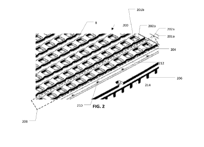
100451 FIG. 2 illustrates a top view of a AESA including a heat sink and
thermal pedestals according to various embodiments.
8
CA 03212426 2023- 9- 15
WO 2022/213097
PCT/ITS2022/071453
100461 An AESA 200 may include a heat sink 214 and a series 208 of
thermal pedestals. The heat sink 214 and the series 208 of thermal pedestals
may be of a unibody, one-piece construction. Two thermal pedestals 201a, 201b
of the series 208 may share a nominally width-wise wall 204. Thermal
pedestals included in the series 208 may share a nominally length-wise wall
210
(a web 210) connecting the thermal pedestals of the series 208.
100471 An Electrically Conductive Thermal Interface Material may be
applied to the top of the heatsink thermal pedestals. The series 208 may be
disposed on an obverse surface 212 of the heat sink 214. Fins 206 may be
disposed on a reverse surface (not shown) of the heat sink 214. Antenna
elements may be disposed on the reverse surface to correspond to the
arrangements of the TRMs ringed by the thermal pedestals. The heat sink 214,
the series 208 and the fins 206 may be of a unibody, one-piece construction. A
PCB may be mounted to a perimeter ledge of the obverse surface 212 around a
plurality of series of the thermal pedestals.
100481 Individual "ringed" thermal pedestals may be tied together, for
example, with a common "web" to improve manufacturability. Metal
manufacturing processes such as casting (expendable or permanent mold
casting), powder metallurgy, deformation, material removal, nontraditional
(lasers, electron beams, chemical erosion, electric discharge and
electrochemical
energy), or joining and assembly may be used to form the thermal pedestals
along with the heat sink and fins as desired.
100491 The wall for the thermal pedestal may be unbroken when
encircling or ringing the void. A ringed void may isolate the electromagnetic
energy of a first TRM from the electromagnetic energy of a second TRM in an
AESA. The wall may be shared between two or more thermal pedestals.
Interconnected thermal pedestals share a fragment of their defining walls with
one another. The defining walls may be a portion of web interconnecting a
plurality of thermal pedestals.
9
CA 03212426 2023- 9- 15
WO 2022/213097
PCT/ITS2022/071453
100501 FIG. 3 illustrates a cross-sectional view of an AESA according to
various embodiments.
100511 An AESA 300 may include a plurality of layers including a radome
302, a polarizer 304, all air gap 306, a PCB 308, and a heat sink 314. TRMs
310 may be disposed on the PCB 308. A TIM 312 may contact the PCB 308
and thermal pedestals 318. Thermal pedestals 318 may extend from a heat sink
314. Fins 316 may extend from the heat sink 314. Heat from the TRMs 310
may be exchanged (convectively) with an ambient environment via the heat
sink 314. In some embodiments, the heat may be conducted from the TRMs
310 to the TIM 312 to the thermal pedestals 318 to the heat sink 314 to the
fins
316. The heat sink 314 may be a heat sink.
100521 Although the subject matter has been described in language
specific to structural features and/or methodological acts, it is to be
understood
that the subject matter in the appended claims is not necessarily limited to
the
specific features or acts described above. Rather, the specific features and
acts
described above are disclosed as example forms of implementing the claims.
Other configurations of the described embodiments are part of the scope of
this
disclosure. Further, implementations consistent with the subject matter of
this
disclosure may have more or fewer acts than as described or may implement
acts in a different order than as shown. Accordingly, the appended claims and
their legal equivalents should only define the invention, rather than any
specific
examples given.
CA 03212426 2023- 9- 15