Note: Descriptions are shown in the official language in which they were submitted.
DUAL PATH SWITCHABLE REPEATER
BACKGROUND
[0001] Repeaters can be used to increase the quality of wireless communication
between a wireless device and a wireless communication access point, such as a
cell tower. Repeaters can increase the quality of the wireless communication
by
amplifying, filtering, and/or applying other processing techniques to uplink
and
downlink signals communicated between the wireless device and the wireless
communication access point.
[0002] As an example, the repeater can receive, via an antenna, downlink
signals
from the wireless communication access point. The repeater can amplify the
downlink signal and then provide an amplified downlink signal to the wireless
device. In other words, the repeater can act as a relay between the wireless
device and the wireless communication access point. As a result, the wireless
device can receive a stronger signal from the wireless communication access
point. Similarly, uplink signals from the wireless device (e.g., telephone
calls and
other data) can be received at the repeater. The repeater can amplify the
uplink
signals before communicating, via an antenna, the uplink signals to the
wireless
communication access point.
BRIEF DESCRIPTION OF THE DRAWINGS
[0003] Features and advantages of the disclosure will be apparent from the
detailed description which follows, taken in conjunction with the accompanying
drawings, which together illustrate, by way of example, features of the
disclosure;
and, wherein:
[0004] FIG. la illustrates a frequency division duplex (FDD) full duplexing
scheme
in accordance with an example;
[0005] FIG. lb illustrates a time division duplex (TDD) half duplexing scheme
in
accordance with an example;
[0006] FIG. 2 illustrates a TDD repeater in a wireless communication system in
accordance with an example;
[0007] FIG. 3a illustrates UL/DL configurations for 3GPP E-UTRA in accordance
1
Date Recue/Date Received 2023-09-22
with an example;
[0008] FIG. 3b-3c illustrates UL/DL configurations for 3GPP 5G NR in
accordance
with an example;
[0009] FIG. 4 illustrates a TDD repeater in accordance with an example;
[0010] FIG. 5a illustrates a TDD repeater with circulators in accordance with
an
example;
[0011] FIG. 5b illustrates a TDD switchable repeater with circulators in
accordance with an example;
[0012] FIG. 5c illustrates a TDD switchable repeater with signal directing
components in accordance with an example;
[0013] FIG. 5d illustrates a TDD switchable repeater with duplexers in
accordance
with an example;
[0014] FIG. 5e illustrates an FDD/TDD dual path repeater having a split mode
and a multiple input multiple output (MIMO) mode in accordance with an
example;
[0015] FIG. 5f illustrates another example embodiment of a TDD repeater with
circulators in accordance with another example;
[0016] FIG. 5g illustrates a block diagram of a software defined filter (SDF)
in
accordance with an example;
[0017] FIG.5h illustrates an example bandpass filter produced by the SDF of
FIG.
Sc in accordance with an example;
[0018] FIG. Si illustrates an example of finite impulse response (FIR)
coefficients
used in the SDF to form the bandpass filter of FIG. 5h in accordance with an
example;
[0019] FIG. 6a illustrates a TDD switchable repeater with switches in
accordance
with an example;
[0020] FIG. 6b illustrates a TDD switchable repeater for TDD multiband
communication in accordance with an example;
[0021] FIG. 7a illustrates a two path multiple input multiple output
(MIMO)/multi-
2
Date Recue/Date Received 2023-09-22
path mode switchable TDD repeater configured to operate in an SBHD mode in
accordance with an example;
[0022] FIG. 7b illustrates a two path MIMO/multi-path mode switchable TDD
repeater configured to operate in a MIMO mode in accordance with an example;
[0023] FIG. 7c illustrates a two path MIMO/multi-path mode switchable TDD
repeater with circulators in accordance with an example;
[0024] FIG. 8a illustrates an E-UTRA downlink radio protocol stack in
accordance
with an example;
[0025] FIG. 8b illustrates an E-UTRA uplink radio protocol stack in accordance
with an example;
[0026] FIG. 8c illustrates an E-UTRA UUDL TDD frame structure in accordance
with an example;
[0027] FIGs. 9a and 9b illustrate a flow chart depicting functionality for
configuring
a dual path repeater having a split mode and a multiple input multiple output
(MIMO) mode in accordance with an example; and
[0028] FIG. 10 illustrates a user equipment (UE) in accordance with an
example.
[0029] Reference will now be made to the exemplary embodiments illustrated,
and specific language will be used herein to describe the same. It will
nevertheless be understood that no limitation of the scope of the invention is
thereby intended.
DETAILED DESCRIPTION
[0030] Before the present invention is disclosed and described, it is to be
understood that this invention is not limited to the particular structures,
process
steps, or materials disclosed herein, but is extended to equivalents thereof
as
would be recognized by those ordinarily skilled in the relevant arts. It
should also
be understood that terminology employed herein is used for the purpose of
describing particular examples only and is not intended to be limiting. The
same
reference numerals in different drawings represent the same element. Numbers
provided in flow charts and processes are provided for clarity in illustrating
steps
and operations and do not necessarily indicate a particular order or sequence.
3
Date Recue/Date Received 2023-09-22
EXAMPLE EMBODIMENTS
[0031] An initial overview of technology embodiments is provided below and
then
specific technology embodiments are described in further detail later. This
initial
summary is intended to aid readers in understanding the technology more
quickly
but is not intended to identify key features or essential features of the
technology
nor is it intended to limit the scope of the claimed subject matter.
[0032] Wireless communication standards use duplexing schemes to separate
the transmission and reception of wireless communication signals. Transmission
of a wireless communication signal from a wireless communication access point,
such as a base station (BS), to a wireless device, such as a user equipment
(UE)
is typically referred to as a downlink (DL) transmission. Reception of a
wireless
communication signal at a BS that was sent from a UE is typically referred to
as
an uplink (UL) transmission. Typical duplexing schemes include Frequency
Division Duplex (FDD) and Time Division Duplex (TDD).
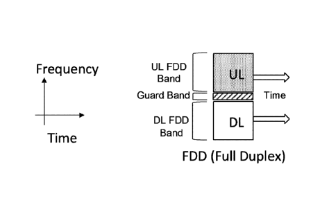
[0033] FIGs. la and lb provide graphical examples of different types of
duplexing
schemes. FIG. la illustrates a typical FDD duplexing scheme. In this example,
an UL FDD band is allocated and is used to continuously transmit an uplink
signal
over the UL FDD band. Similarly, a DL FDD band is allocated to continuously
transmit a downlink signal over the DL FDD band. Because the UL and DL
signals can be transmitted continuously and simultaneously, the FDD duplexing
scheme is referred to as full duplex.
[0034] The UL FDD band and DL FDD band in FIG. la are separated by a guard
band. The guard band is used to enable a receiver to receive the UL and DL
signals without interference from the adjacent signal.
[0035] FIG. lb illustrates a typical TDD duplexing scheme. In this example, a
TDD band is used to transmit an UL signal for the duration of an UL time slot.
In
contrast with the FDD scheme, the bandwidth for the UL signal does not have to
be shared with a bandwidth for a DL signal. Rather, the TDD band can comprise
the full frequency allocation for the selected TDD band. A DL signal can be
transmitted over the full TDD band for the duration of the DL time slot.
Because
transmission of the UL signal and DL signal is not simultaneous, and is shared
in
time, the TDD duplexing scheme is referred to as half duplex.
4
Date Recue/Date Received 2023-09-22
[0036] A guard period is designated in FIG. 1b between the UL time slot and
the
DL time slot. The guard period is used to allow a transceiver time to switch
between transmission and reception modes. In addition, the guard period is
selected based on the time of flight for the UL or DL signal between the BS
and
the UE.
[0037] Repeaters can increase the quality of wireless communication between a
wireless device, such as a UE and a wireless communication access point, such
as a BS, by amplifying, filtering, or applying other processing techniques to
uplink
and downlink signals communicated between the wireless device and the
wireless communication access point.
[0038] In one example, as illustrated in FIG. 2, a time division duplex (TDD)
repeater 200 can include a first port 202 (e.g., a server port), a second port
204
(e.g., a donor port), and one or more amplification paths (not shown) coupled
between the first port 202 and the second port 204. The TDD repeater is
configured to be connected to a donor antenna 205 and a server antenna 203 via
the second port 204 and the first port 202, respectively. The TDD repeater 200
can be configured to receive a TDD UL signal from a UE 210 and send the TDD
UL signal to a node 220 and/or a node 230. The TDD repeater 200 can be
configured to receive a TDD DL signal from the node 220 and/or node 230 at the
second port 204 and send the TDD DL signal to the UE 210.
[0039]
[0040] The repeater 200 can boost signals configured based on selected
wireless
standards, such as the Third Generation Partnership Project (3GPP) Evolved
Universal Terrestrial Radio Access (E-UTRA) Release 8, 9, 10, 11, 12, 13, 14,
15,
16, or 17 standards or Institute of Electronics and Electrical Engineers
(IEEE)
802.16. The E-UTRA standards were previously referred to as fourth generation
(4G) standards, with Releases 10-17 also referred to as 4G Long Term Evolution
(LTE) standards. The terms E-UTRA, 4G, and LTE are used synonymously in
this document, unless otherwise noted. In one configuration, the repeater 200
can boost signals for 3GPP LTE Release 17.4.0 (January 2022) or other desired
releases.
[0041] The repeater 200 can boost signals from the 3GPP Technical
Specification
5
Date Recue/Date Received 2023-09-22
(TS) 36.101 (Release 17 January 2021) Evolved Universal Terrestrial Radio
Access (E-UTRA) TDD frequency bands. The repeater 200 may also be
configured to boost E-UTRA FDD frequency bands. In addition, the repeater 200
can boost selected frequency bands based on the country or region in which the
repeater is used, including any of TDD bands 33-53, or other bands, as
disclosed
in 3GPP TS 36.104 V17.4.0 (January 2022), and depicted in Table 1.
Table 1:
6
Date Recue/Date Received 2023-09-22
E-UTRA Uplink (UL) operating band Downlink (DL) operating band Duplex
Operating BS receive BS transmit Mode
Band UE transmit UE receive
FuL _low ¨ FUL_high FDL_low ¨ FDL_high
1 1920 MHz ¨ 1980 MHz 2110 MHz ¨ 2170 MHz FDD
2 1850 MHz ¨ 1910 MHz 1930 MHz ¨ 1990 MHz FDD
3 1710 MHz ¨ 1785 MHz 1805 MHz ¨ 1880 MHz FDD
4 1710 MHz ¨ 1755 MHz 2110 MHz ¨ 2155 MHz FDD
824 MHz ¨ 849 MHz 869 MHz ¨ 894MHz FDD
6 830 MHz 840 MHz 875 MHz 885 MHz
FDD
(NOTE 1) ¨ ¨
7 2500 MHz ¨ 2570 MHz 2620 MHz ¨ 2690 MHz FDD
8 880 MHz ¨ 915 MHz 925 MHz ¨ 960 MHz FDD
1749.9 ¨ ¨ FDD
9 1784.9 MHz 1844.9 MHz 1879.9 MHz
MHz
1710 MHz ¨ 1770 MHz 2110 MHz ¨ 2170 MHz FDD
1427.9 ¨ 1447.9 MHz 1475.9 MHz ¨ 1495.9 MHz FDD
11
MHz
12 699 MHz ¨ 716 MHz 729 MHz ¨ 746 MHz FDD
13 777 MHz ¨ 787 MHz 746 MHz ¨ 756 MHz FDD
14 788 MHz ¨ 798 MHz 758 MHz ¨ 768 MHz FDD
Reserved Reserved FDD
16 Reserved Reserved FDD
17 704 MHz ¨ 716 MHz 734 MHz ¨ 746 MHz FDD
18 815 MHz ¨ 830 MHz 860 MHz ¨ 875 MHz FDD
19 830 MHz ¨ 845 MHz 875 MHz ¨ 890 MHz FDD
832 MHz ¨ 862 MHz 791 MHz ¨ 821 MHz FDD
21 1447.9 ¨ 1462.9 MHz 1495.9 MHz ¨ 1510.9 MHz FDD
MHz
22 3410 MHz ¨ 3490 MHz 3510 MHz ¨ 3590 MHz FDD
231 2000 MHz ¨ 2020 MHz 2180 MHz ¨ 2200 MHz FDD
249 1626.5 ¨ 1660.5 MHz 1525 MHz ¨ 1559 MHz
FDD
MHz
1850 MHz ¨ 1915 MHz 1930 MHz ¨ 1995 MHz FDD
26 814 MHz ¨ 849 MHz 859 MHz ¨ 894 MHz FDD
27 807 MHz ¨ 824 MHz 852 MHz ¨ 869 MHz FDD
28 703 MHz ¨ 748 MHz 758 MHz ¨ 803 MHz FDD
717 MHz ¨ 728 MHz FDD
29 N/A (NOTE
2)
2305 MHz ¨ 2315 MHz 2350 MHz ¨ 2360 MHz FDD
31 452.5 MHz ¨ 457.5 MHz 462.5 MHz ¨ 467.5 MHz FDD
N/A 1452 MHz ¨ 1496 MHz FDD
32 (NOTE
2)
33 1900 MHz ¨ 1920 MHz 1900 MHz ¨ 1920 MHz TDD
34 2010 MHz ¨ 2025 MHz 2010 MHz ¨ 2025 MHz TDD
1850 MHz ¨ 1910 MHz 1850 MHz ¨ 1910 MHz TDD
36 1930 MHz ¨ 1990 MHz 1930 MHz ¨ 1990 MHz TDD
37 1910 MHz ¨ 1930 MHz 1910 MHz ¨ 1930 MHz TDD
38 2570 MHz ¨ 2620 MHz 2570 MHz ¨ 2620 MHz TDD
39 1880 MHz ¨ 1920 MHz 1880 MHz ¨ 1920 MHz TDD
2300 MHz ¨ 2400 MHz 2300 MHz ¨ 2400 MHz TDD
41 2496 MHz ¨ 2690 MHz 2496 MHz ¨ 2690 MHz TDD
42 3400 MHz ¨ 3600 MHz 3400 MHz ¨ 3600 MHz TDD
43 3600 MHz ¨ 3800 MHz 3600 MHz ¨ 3800 MHz TDD
44 703 MHz ¨ 803 MHz 703 MHz ¨ 803 MHz TDD
1447 MHz ¨ 1467 MHz 1447 MHz ¨ 1467 MHz TDD
46 5150 MHz ¨ 5925 MHz 5150 MHz ¨ 5925 MHz TDD
(NOTE
3,
NOTE
4)
7
Date Recue/Date Received 2023-09-22
E-UTRA Uplink (UL) operating band Downlink (DL) operating band Duplex
Operating BS receive BS transmit Mode
Band UE transmit UE receive
FuLlow FUL_high FDL_low FDL_high
47 5855 MHz ¨ 5925 MHz 5855 MHz ¨ 5925 MHz
TDD
48 3550 MHz ¨ 3700 MHz 3550 MHz ¨ 3700 MHz
TDD
49 3550 MHz ¨ 3700 MHz 3550 MHz ¨ 3700 MHz
TDD
(NOTE
8)
50 1432 MHz - 1517 MHz 1432 MHz - 1517 MHz
TDD
51 1427 MHz - 1432 MHz 1427 MHz - 1432 MHz
TDD
52 3300 MHz - 3400 MHz 3300 MHz - 3400 MHz
TDD
53 2483.5 - 2495 MHz 2483.5 MHz - 2495 MHz
TDD
MHz
65 1920 MHz ¨ 2010 MHz 2110 MHz ¨ 2200 MHz
FDD
66 1710 MHz ¨ 1780 MHz 2110 MHz ¨ 2200 MHz
FDD
(NOTE
5)
67 N/A 738 MHz ¨ 758 MHz FDD
(NOTE
2)
68 698 MHz ¨ 728 MHz 753 MHz ¨ 783 MHz FDD
69 N/A 2570 MHz ¨ 2620 MHz
FDD
(NOTE
2)
70 1695 MHz ¨ 1710 MHz 1995 MHz ¨ 2020 MHz
FDD6
71 663 MHz ¨ 698 MHz 617 MHz ¨ 652 MHz FDD
72 451 MHz ¨ 456 MHz 461 MHz ¨ 466 MHz FDD
73 450 MHz ¨ 455 MHz 460 MHz ¨ 465 MHz FDD
74 1427 MHz ¨ 1470 MHz 1475 MHz ¨ 1518 MHz
FDD
75 N/A 1432 MHz ¨ 1517 MHz
FDD
(NOTE
2)
76 N/A 1427 MHz ¨ 1432 MHz
FDD
(NOTE
2)
85 698 MHz ¨ 716 MHz 728 MHz ¨ 746 MHz
FDD
87 410 MHz ¨ 415 MHz 420 MHz ¨ 425 MHz
FDD
88 412 MHz ¨ 417 MHz 422 MHz ¨ 427 MHz
FDD
NOTE 1: Band 6, 23 are not applicable.
NOTE 2: Restricted to E-UTRA operation when carrier aggregation is configured.
The
downlink operating band is paired with the uplink operating band (external) of
the carrier aggregation configuration that is supporting the configured Pcell.
NOTE 3: This band is an unlicensed band restricted to licensed-assisted
operation using
Frame Structure Type 3.
NOTE 4: Band 46 is divided into four sub-bands as in Table 5.5-1A.
NOTE 5: The range 2180 ¨ 2200 MHz of the DL operating band is restricted to E-
UTRA
operation when carrier aggregation is configured.
NOTE 6: The range 2010-2020 MHz of the DL operating band is restricted to E-
UTRA
operation when carrier aggregation is configured and TX-RX separation is 300
MHz. The range 2005-2020 MHz of the DL operating band is restricted to E-
UTRA operation when carrier aggregation is configured and TX-RX separation
is 295 MHz.
NOTE 7: Void
NOTE 8: This band is restricted to licensed-assisted operation using Frame
Structure
Type 3.
NOTE 9: DL operation is restricted to 1526-1536 MHz frequency range. UL
operation is
restricted to 1627.5¨ 1637.5 MHz and 1646.5¨ 1656.5 MHz per FCC Order
DA 20-48.
[0042] In another configuration, the repeater 200 can boost TDD signals from
the
3GPP Technical Specification (TS) 38.104 (Release 17 January 2021) bands or
8
Date Recue/Date Received 2023-09-22
5G frequency bands, referred to as new radio operating bands. These bands
typically begin with the prefix "n". In addition, the repeater 200 can boost
selected frequency bands based on the country or region in which the repeater
is
used, including any of TDD bands n34 ¨ n53, n77-n79, n90, or n96 in frequency
range 1 (FR1), n257 ¨ n262 in frequency range 2 (FR2), or other bands, as
disclosed in 3GPP TS 38.104 V17.4.0 (January 2022), and depicted in Table 2
and Table 3:
Table 2:
9
Date Recue/Date Received 2023-09-22
NR Uplink (UL) operating band Downlink (DL) operating band Duplex
operating BS receive / UE transmit BS transmit! UE
receive mode
band FuL,low ¨ FUL,high FDL,low ¨ FDL,high
n1 1920 MHz¨ 1980 MHz 2110 MHz ¨ 2170 MHz FDD
n2 1850 MHz ¨ 1910 MHz 1930 MHz ¨ 1990 MHz FDD
n3 1710 MHz ¨ 1785 MHz 1805 MHz ¨ 1880 MHz FDD
n5 824 MHz ¨849 MHz 869 MHz ¨894 MHz FDD
n7 2500 MHz ¨ 2570 MHz 2620 MHz ¨ 2690 MHz FDD
n8 880 MHz ¨915 MHz 925 MHz ¨960 MHz FDD
n12 699 MHz ¨ 716 MHz 729 MHz ¨ 746 MHz FDD
n13 777 MHz ¨787 MHz 746 MHz ¨756 MHz FDD
n14 788 MHz ¨798 MHz 758 MHz ¨768 MHz FDD
n18 815 MHz ¨830 MHz 860 MHz ¨875 MHz FDD
n20 832 MHz ¨862 MHz 791 MHz ¨821 MHz FDD
n247 1626.5 MHz¨ 1660.5 MHz 1525 MHz¨ 1559
MHz FDD
n25 1850 MHz ¨ 1915 MHz 1930 MHz ¨ 1995 MHz FDD
n26 814 MHz ¨849 MHz 859 MHz ¨894 MHz FDD
n28 703 MHz ¨ 748 MHz 758 MHz ¨803 MHz FDD
n29 N/A 717 MHz ¨ 728 MHz SDL
n30 2305 MHz ¨2315 MHz 2350 MHz ¨2360 MHz FDD
n34 2010 MHz ¨ 2025 MHz 2010 MHz ¨ 2025 MHz TDD
n38 2570 MHz ¨2620 MHz 2570 MHz ¨2620 MHz TDD
n39 1880 MHz ¨ 1920 MHz 1880 MHz ¨ 1920 MHz TDD
n40 2300 MHz ¨2400 MHz 2300 MHz ¨2400 MHz TDD
n41 2496 MHz ¨2690 MHz 2496 MHz ¨2690 MHz TDD
n46 5150 MHz ¨5925 MHz 5150 MHz ¨5925 MHz TDD3
n48 3550 MHz ¨3700 MHz 3550 MHz ¨3700 MHz TDD
n50 1432 MHz ¨ 1517 MHz 1432 MHz ¨ 1517 MHz TDD
n51 1427 MHz ¨ 1432 MHz 1427 MHz ¨ 1432 MHz TDD
n53 2483.5 MHz ¨2495 MHz 2483.5 MHz ¨ 2495 MHz TDD
n65 1920 MHz ¨ 2010 MHz 2110 MHz ¨ 2200 MHz FDD
n66 1710 MHz ¨ 1780 MHz 2110 MHz ¨ 2200 MHz FDD
n67 N/A 738 MHz ¨ 758 MHz SDL
n70 1695 MHz¨ 1710 MHz 1995 MHz ¨ 2020 MHz FDD
n71 663 MHz ¨698 MHz 617 MHz ¨652 MHz FDD
n74 1427 MHz ¨ 1470 MHz 1475 MHz ¨ 1518 MHz FDD
n75 N/A 1432 MHz ¨ 1517 MHz SDL
n76 N/A 1427 MHz ¨ 1432 MHz SDL
n77 3300 MHz ¨4200 MHz 3300 MHz ¨4200 MHz TDD
n78 3300 MHz ¨3800 MHz 3300 MHz ¨3800 MHz TDD
n79 4400 MHz ¨ 5000 MHz 4400 MHz ¨ 5000 MHz TDD
n80 1710 MHz ¨ 1785 MHz N/A SUL
n81 880 MHz ¨ 915 MHz N/A SUL
n82 832 MHz ¨862 MHz N/A SUL
n83 703 MHz ¨748 MHz N/A SUL
n84 1920 MHz ¨ 1980 MHz N/A SUL
n85 698 MHz ¨ 716 MHz 728 MHz ¨ 746 MHz FDD
n86 1710 MHz ¨ 1780 MHz N/A SUL
n89 824 MHz ¨849 MHz N/A SUL
n90 2496 MHz ¨2690 MHz 2496 MHz ¨2690 MHz TDD
n91 832 MHz ¨ 862 MHz 1427 MHz ¨ 1432 MHz FDD2
n92 832 MHz ¨ 862 MHz 1432 MHz¨ 1517 MHz FDD2
n93 880 MHz ¨ 915 MHz 1427 MHz ¨ 1432 MHz FDD2
n94 880 MHz ¨ 915 MHz 1432 MHz¨ 1517 MHz FDD2
n951 2010 MHz ¨ 2025 MHz N/A SUL
n964 5925 MHz ¨ 7125 MHz 5925 MHz ¨ 7125 MHz TDD3
n975 2300 MHz ¨2400 MHz N/A SUL
n985 1880 MHz ¨ 1920 MHz N/A SUL
n996 1626.5 MHz -1660.5 MHz N/A SUL
Date Recue/Date Received 2023-09-22
NOTE 1: This band is applicable in China only.
NOTE 2: Variable duplex operation does not enable dynamic variable duplex
configuration
by the network, and is used such that DL and UL frequency ranges are supported
independently in any valid frequency range for the band.
NOTE 3: This band is restricted to operation with shared spectrum channel
access as
defined in [20].
NOTE 4: This band is applicable in the USA only subject to FCC Report and
Order [FCC 20-
51].
NOTE 5: The requirements for this band are applicable only where no other NR
or E-UTRA
TDD operating band(s) are used within the frequency range of this band in the
same geographical area. For scenarios where other NR or E-UTRA TDD operating
band(s) are used within the frequency range of this band in the same
geographical
area, special co-existence requirements may apply that are not covered by the
3GPP specifications.
NOTE 6: UL operation is restricted to 1627.5¨ 1637.5 MHz and 1646.5¨ 1656.5
MHz per
FCC Order DA 20-48.
NOTE 7: DL operation is restricted to 1526-1536 MHz frequency range. UL
operation is
restricted to 1627.5¨ 1637.5 MHz and 1646.5¨ 1656.5 MHz per FCC Order DA
20-48.
Table 3:
NR Uplink (UL) and Downlink (DL) Duplex
operating operating band mode
band BS transmit/receive
UE transmit/receive
FuLoow ¨ FUL,high
FDL,low FDL,high
n257 26500 MHz ¨ 29500 MHz TDD
n258 24250 MHz ¨ 27500 MHz TDD
n259 39500 MHz ¨43500 MHz TDD
n260 37000 MHz ¨40000 MHz TDD
n261 27500 MHz ¨ 28350 MHz TDD
n262 47200 MHz ¨48200 MHz TDD
[0043] For E-UTRA, each operating band can be divided into different channel
bandwidths, depending on the size of the operating band. The channel
bandwidths are disclosed in 3GPP TS 36.104 V17.4.0 (January 2022), and
depicted in Table 4. The table shows the number of physical resource blocks
(NRB) in each channel. The definition of a physical resource block (PRB) for
EUTRA, also called a resource block (RB) is well known and is defined in 3GPP
TS 36.211 V 17.4.0 (January 2022).
Table 4:
Channel
bandwidth 1.4 3 5 10 15 20
BWChannel [M Hz]
Transmission
bandwidth 6 15 25 50 75 100
configuration NRB
11
Date Recue/Date Received 2023-09-22
[0044] For 5G, the New Radio (NR) operating bands can also be divided into
different channel bandwidths. 5G was designed to have more flexibility,
allowing
for a number of different modalities than previous generations of cellular
communication. Each NR operating band has different channel bandwidths that
can be used. Each channel can include different subcarrier spacing (SCS).
Table 5, shown below, provides an example of channel bandwidths for the NR
operating bands in FR 1 and the available SCS for each NR operating band. The
channel bandwidths are disclosed in 3GPP TS 36.101-1 V17.4.0 (January 2022).
Table 6 shows the NR operating bands in FR 2, as disclosed in 3GPP TS 36.101-
2 V17.4.0 (January 2022)
Table 5:
NR Band SCS UE Channel bandwidth (MHz)
(kHz) 5 10 15 20 25 30 35 40 45 50 60 70 80 90 100
n1 15 5 10 15 20 25 30 40 454 50
30 10 15 20 25 30 40 454 50
60 10 15 20 25 30 40 454 50
n2 15 5 10 15 20 25 30 354 40
30 10 15 20 25 30 354 40
60 10 15 20 25 30 354 40
n3 15 5 10 15 20 25 30 354 40 454 50
30 10 15 20 25 30 354 40 454 50
60 10 15 20 25 30 354 40 454 50
n5 15 5 10 15 20 253
30 10 15 20 253
n7 15 5 10 15 20 25 30 354 40 50
30 10 15 20 25 30 354 40 50
60 10 15 20 25 30 354 40 50
5 353,
n8 15 10 15 20 4
10 353,
30 15 20 4
n12 15 5 10 15
30 10 15
n13 15 5 10
30 10
n14 15 5 10
30 10
n18 15 5 10 15
30 10 15
n20 15 5 10 15 20
30 10 15 20
60
12
Date Recue/Date Received 2023-09-22
NR Band SCS UE Channel bandwidth (MHz)
(kHz) 5 10 15 20 25 30 35 40 45 50 60 70 80 90 100
n24 15 5 10
30 10
60 10
15 5 10 15 20 25 30 354 40 453'
n25 4
30 10 15 20 25 30 354 40 453,
4
60 10 15 20 25 30 354 40 453,
4
n26 15 5 10 15 20
30 10 15 20
n28 15 5 10 15 207 307
30 10 15 207 307
n29 15 5 10
30 10
n30 15 5 10
30 10
n34 15 5 10 15
30 10 15
60 10 15
n38 15 5 1015 15 2015 25 3015 4015
30 1015 15 2015 25 3015 4015
60 1015 15 2015 25 3015 4015
n39 15 5 10 15 20 25 30 40
30 10 15 20 25 30 40
60 10 15 20 25 30 40
n40 15 55 10 15 20 25 30 40 50
30 10 15 20 25 30 40 50 60 70 80 90
100
60 10 15 20 25 30 40 50 60 70 80 90
100
n41 15 10 15 20 30 40 50
30 10 15 20 30 40 50 60 70 80 90 100
60 10 15 20 30 40 50 60 70 80 90 100
n46 15 105 20 40
30 105 20 40 60 80
60 105 20 40 60 80
n47 15 1015 2015 3015 4015
30 1015 2015 3015 4015
60 1015 2015 3015 4015
n48 15 55 10 15 20 30 40 506
30 10 15 20 30 40
506 606 706 806 906, 1006
4
60 10 15 20 30 40
506 606 706 806 906' 1
006
4
n50 15 55 10 15 20 30 40 50
30 10 15 20 30 40 50 60 803
60 10 15 20 30 40 50 60 803
n51 15 5
60
n53 15 5 10
30 10
13
Date Recue/Date Received 2023-09-22
NR Band SCS UE Channel bandwidth (MHz)
(kHz) 5 10 15 20 25 30 35 40 45 50 60 70 80 90 100
60 10
n65 15 5 10 15 20 50
30 10 15 20 50
60 10 15 20 50
n66 15 5 10 15 20 25 30 354 40 454
30 10 15 20 25 30 354 40 454
60 10 15 20 25 30 354 40 454
n67 15 5 10 15 20
30 10 15 20
n70 15 5 10 15 203 253
30 10 15 203 253
60 10 15 203 253
5 253 303 353,
n71 15 10 15 20 4
10 15 20 253 303 353,
4
n74 15 5 10 15 20
30 10 15 20
60 10 15 20
n75 15 5 10 15 20 25 30 40 50
30 10 15 20 25 30 40 50
60 10 15 20 25 30 40 50
n76 15 5
60
n77 15 10 15 20 25 30 40 50
30 10 15 20 25 30 40 50 60 704 80 904 100
60 10 15 20 25 30 40 50 60 704 80 904 100
n78 15 10 15 20 25 30 40 50
30 10 15 20 25 30 40 50 60 704 80 90 100
60 10 15 20 25 30 40 50 60 704 80 90 100
n79 15 10 20 30 40 50
30 10 20 30 40 50 60 704 80 90 100
60 10 20 30 40 50 60 704 80 90 100
n80 15 5 10 15 20 25 30 40
30 10 15 20 25 30 40
60 10 15 20 25 30 40
n81 15 5 10 15 20
30 10 15 20
n82 15 5 10 15 20
30 10 15 20
n83 15 5 10 15 20 307
30 10 15 20 307
n84 15 5 10 15 20 25 30 40 50
30 10 15 20 25 30 40 50
60 10 15 20 25 30 40 50
n85 15 5 10 15
30 10 15
n86 15 5 10 15 20 40
14
Date Recue/Date Received 2023-09-22
NR Band SCS UE Channel bandwidth (MHz)
(kHz) 5 10 15 20 25 30 35 40 45 50 60 70 80 90 100
30 10 15 20 40
60 10 15 20 40
n89 15 5 10 15 20
30 10 15 20
60 50
n90 15 10 15 20 30 40 50
30 10 15 20 30 40 50 60 80 90 100
60 10 15 20 30 40 50 60 80 90 100
n91 15 5 108
60
n92 15 5 10 15 20
30 10 15 20
n93 15 5 108
60
n94 15 5 10 15 20
30 10 15 20
n95 15 5 10 15
30 10 15
60 10 15
n96 15 20 40
30 20 40 60 80
60 20 40 60 80
n97 15 5 10 15 20 25 30 40 50
30 10 15 20 25 30 40 50 60 70 80 90 100
60 10 15 20 25 30 40 50 60 70 80 90 100
n98 15 5 10 15 20 25 30 40
30 10 15 20 25 30 40
60 10 15 20 25 30 40
15 5 10
n99 30 10
60 10
NOTE 1: Void.
NOTE 2: Void.
NOTE 3: This UE channel bandwidth is applicable only to downlink.
NOTE 4: This UE channel bandwidth is optional in this release of the
specification.
NOTE 5: For this bandwidth, the minimum requirements are restricted to
operation when carrier is configured as an SCell
part of DC or Carrier Aggregation (CA) configuration.
NOTE 6: For this bandwidth, the minimum requirements are restricted to
operation when carrier is configured as a
downlink Secondary Cell (SCell) part of CA configuration.
NOTE 7: For the 20 MHz bandwidth, the minimum requirements are specified for
NR UL carrier frequencies confined to
either 713-723 MHz or 728-738 MHz. For the 30MHz bandwidth, the minimum
requirements are specified for
NR UL transmission bandwidth configuration confined to either 703-733 or 718-
748 MHz.
NOTE 8: This UE channel bandwidth is applicable only to uplink.
NOTE 9: Void.
NOTE 10: These UE channel bandwidths are applicable to sidelink operation
Date Recue/Date Received 2023-09-22
Table 6:
UE channel bandwidth
Operating SCS (MHz)
band (kHz)
50 100 200 4001
n257 60 50 100 200
120 50 100 200 400
n258 60 50 100 200
120 50 100 200 400
n259 60 50 100 200
120 50 100 200 400
n260 60 50 100 200
120 50 100 200 400
n261 60 50 100 200
120 50 100 200 400
n262 60 50 100 200
120 50 100 200 400
NOTE 1: This UE channel bandwidth is optional in
this release of the specification.
[0045] The 3GPP E-UTRA standard (Rel. 8-17) is configured to transmit and
receive TDD signals based on a subframe granularity. A predetermined uplink-
downlink configuration (UL/DL Config) can be used to determine which
subframes are used for uplink and which subframes are used for downlink. In an
example, the 3GPP E-UTRA frame structure is configured with a radio frame of
length 10 milliseconds (ms) that can include two half-frames of length 5 ms
each.
Each half-frame can include 5 subframes of length 1 ms. Each subframe can
include two slots of length 0.5 ms each. The uplink-downlink configuration in
a
cell can vary between frames and controls in which a subframes uplink or
downlink transmission can take place in the current frame. The supported
uplink-
downlink configurations can be configured as listed in FIG. 3a where, for each
subframe in a radio frame, "D" can denote a downlink subframe reserved for
downlink transmissions, "U" can denote an uplink subframe reserved for uplink
transmissions, and "S" can denote a special subframe. The special subframes
are used to communicate control information. Uplink-downlink configurations
with both 5 ms and 10 ms downlink-to-uplink switch-point periodicity can be
supported. In the case of 5 ms downlink-to-uplink switch-point periodicity,
the
special subframe can exist in both half-frames (slots). In the case of 10 ms
downlink-to-uplink switch-point periodicity, the special subframe can exist in
the
first half-frame only. In the 3GPP E-UTRA Version 8 standard, there are seven
different preconfigured uplink-downlink configurations, numbered between 0 and
6, as illustrated in FIG. 3a.
16
Date Recue/Date Received 2023-09-22
[0046] A 3GPP E-UTRA base station can be configured to transmit which of the
seven UL/DL configurations will be used. In another example, a repeater can be
configured to receive the UL/DL configuration indication from the base
station.
The configuration information is typically transmitted from the base station
via
higher layer signaling, such as radio resource control (RRC) signaling. In
another
example, for each radio frame, the repeater can demodulate and/or decode
control information in a physical downlink control channel (PDCCH) or physical
downlink shared channel (PDSCH) using a downlink control information (DCI)
format type to receive UL/DL configuration. In one example, a repeater can be
coupled to a TDD switch controller, such as a TDD sync detection module (SDM)
or a modem that can be used to receive the 3GPP LTE UL/DL configuration
information from a base station for a cellular signal associated with the base
station. Alternatively, a UE can receive and decode the UL/DL configuration
information from the base station (i.e. evolved Node B or eNB or next
generation
Node B or gNB) and communicate the UL/DL configuration information to the
repeater via a wireless transmission using a predetermined wireless standard,
such as Bluetooth or Wi-Fi (IEEE 802.11).
[0047] FIGS. 3b and 3c provide example UL/DL configurations for 3GPP 5G
communication, as described in 3GPP 38.213 V 17Ø0 (December 2021). In 5G
NR communication systems, a frame of 10 ms duration can include ten
subframes of 1 ms duration, as in the E-UTRA standard. However, in the NR
standard, each frame can comprise 2u slots, where U is 1, 2, 3 or 4 and is a
multiple of the SCS of 15 kilohertz (kHz). Each slot can include 14 orthogonal
frequency division multiplexing (OFDM) symbols. The OFDM symbols in each
slot can be classified as downlink 'D', flexible 'F', or uplink 'Ll. In a slot
in a
downlink frame, downlink transmissions can only occur in 'downlink' or
'flexible'
symbols. In a slot in an uplink frame, the uplink transmission can only occur
in
'uplink' or 'flexible' symbols.
[0048] The UL/DL slot configurations for 5G NR are illustrated in FIGS. 3b and
3c.
A slot format can be identified by a corresponding format index ranging from 0
to
55 where 'D' can denote a symbol for downlink transmission, 'Ll can a symbol
for
uplink transmission, and 'F' can denote a flexible symbol. In another example,
a
17
Date Recue/Date Received 2023-09-22
slot format index 255 can have a slot format as disclosed in 3GPP TS 38.213
V17Ø0 (2021-12). Slot index formats 56¨ 254 are currently reserved.
[0049] In another example, a repeater can be configured to receive the UL/DL
configuration for the slot format per slot in one or more higher layer
parameters
via higher layer signaling (such as RRC signaling). The higher layer
parameters
can provide a reference subcarrier spacing, a slot configuration period, a
number
of downlink symbols, or a number of uplink symbols. In another example, the
repeater can be configured to receive a higher layer parameter that can
override
only the flexible symbols per slot over a number of slots as provided by
another
higher layer parameter.
[0050] In another example, a repeater can be configured to receive a higher
layer
parameter that includes a set of slot format combinations, in which each slot
format combination can include one or more slot formats as illustrated in
FIGS.
3b and 3c. In another example, a repeater can be configured to demodulate
and/or decode control information on a physical control channel or physical
shared channel that includes a slot format. In one example, async detection
module (SDM) or modem can be used to receive the 3GPP 5G UL/DL
configuration information from a base station for a cellular signal associated
with
the base station. The SDM / modem is discussed near the end of the
specification.
[0051] A repeater, can be configured to amplify and filter a time division
duplex
(TDD) frequency band in a wireless communications system for transmission
from a wireless device, such as a UE, to a base station, such as a gNode B
(gNB) and for transmission from a base station to the wireless device. The
repeater can be coupled to a TDD sync detection module (SDM) or a modem that
is configured to receive an UL/DL configuration and timing information for a
TDD
signal received at the repeater. A TDD repeater can use a TDD SDM to control
switching and filtering of the TDD signals between transmission from a
wireless
device to a base station (e.g., an uplink (UL) transmission) and transmission
from
a base station to a wireless device (e.g., a downlink (DL) transmission). An
SDM
may be configured to identify the UL/DL configuration for multiple signals.
Alternatively, a repeater can include multiple SDMs, with each SDM configured
to
18
Date Recue/Date Received 2023-09-22
determine the UUDL configuration for a single TDD signal in a single TDD
operating band.
[0052] FIG. 4 provides an example of a TDD repeater 400 that can use an SDM
or modem to switch a first switch, such as a single pull double throw (SPDT1)
between a TDD UL path and a TDD DL path. The SDM or modem can also
switch a second switch, such as SPDT2 between the TDD UL path and the TDD
DL path. Each path can include a low noise amplifier (LNA), a variable
attenuator, a TDD bandpass filter (BPF) configured for the TDD operating band,
and a power amplifier (PA). In one example, a TDD UL signal can be received
from the UE at the server antenna, filtered by the BPF, and switched to the
TDD
UL path for amplification and filtering, then switched for additional bandpass
filtering and transmitted from the donor antenna to a base station. Similarly,
a
TDD DL signal transmitted from a base station, such as an eNB for E-UTRA or a
gNB for 5G, and received at the donor antenna, filtered in the bandpass
filter,
switched at SPDT2 to the TDD DL path for amplification and filtering, then
switched using SPDT 1 for additional bandpass filtering and directed to the
server
antenna for transmission to a UE.
[0053] FIG. 5a provides an example of an alternative embodiment of a TDD
repeater 500. In this example, the repeater 500 includes circulators 506, 508
instead of using switches, such as the SPDT1 and SPDT2 of the repeater of FIG.
4. In addition, software defined filters (SDF) 510, 512 are configured to
filter the
TDD signals received at the donor port 504 from the donor antenna 505 and at
the server port 502 from the server antenna 503. The SDFs 510, 512 can be
communicatively coupled to an SDM/modem 514 via a controller 516. The SDFs
510, 512 can be separate processors or a single processor used for both of a
first
amplification and filtering path 537a and a second amplification and filtering
path
527a. The SDM/modem can provide an UL/DL configuration and timing
information to the SDF 510, 512. In one embodiment, a single SDM/modem 514
can provide the UL/DL configuration and timing to both SDFs 510, 512.
Alternatively, separate SDMs or modems (i.e. two SDMs, two modems, or one
SDM and one modem) can provide the UL/DL configuration and timing to the
SDFs 510, 512.
19
Date Recue/Date Received 2023-09-22
[0054] In the example illustrated in FIG. 4, the switches SPDT1 and SPDT2 are
configured with the SDM so that the TDD UL signals are routed along the TDD
UL path, and the TDD DL signals are routed along the TDD DL path. In contrast,
in the example of FIG. 5a, the circulators 506, 508 operate differently than
the
switches. A circulator is a radio frequency device with 3 or 4 ports. A signal
entering a port in the circulator will exit at the next port. In this example,
the
fourth port is set to ground. A circulator provides about 16 to 25 dB of
isolation
between each port in the circulator. A repeater typically requires a greater
level of
total loop isolation/attenuation than the total amount of loop gain of the
repeater.
If the loop gain (as measured in decibels) is greater than the loop
isolation/attenuation (as measured in decibels), then the repeater can
destructively resonate or oscillate and cause problems in the communication
network.
[0055] A switched TDD repeater 400, as illustrated in FIG. 4, has the
advantage
of being able to disable components in the 'off' path. This allows the
repeater to
operate without the need for the switches to provide all of the necessary
isolation.
Disabling components reduces the overall loop gain and increases the
attenuation.
[0056] In contrast, a bi-directional TDD repeater, such as the TDD repeater
500
illustrated in the example of FIG. 5a, is designed to obtain substantially all
of the
isolation/attenuation from the circulators 506, 508 and SDF(s) 510, 512. The
SDF(s) 510, 512 can provide filters with a sufficiently sharp roll-off to
effectively
create a guard band between the UL and DL channels of TDD signals with
different frequencies.
[0057] The use of circulators 506 and 508 in FIG. 5a typically provide about
16 to
25 dB of isolation and 0.2 to 1.0 dB of insertion loss (IL) as the signal
passes
through the circulator. The passband filters 528 and 518 can also provide some
isolation, such as 0.5 dB to 3 dB for a typical passband filter. The variable
attenuators 540 and 530 can be used to reduce the amplitude of the signals in
the TDD UL path and TDD DL path.
[0058] In one example, a gain of 20 dB can be assumed per LNA (528, 538) and
PA (542, 544). An additional loss of approximately 2 dB per passive component
Date Recue/Date Received 2023-09-22
(i.e. 518, 528, 530, 540) provides for 8 dB of loss, for a total loop gain of
72 dB.
[0059] Each SDF 510, 512 can provide 30 to 50 dB of isolation. Each circulator
506, 508 can provide 16 dB of isolation. With 30 dB of isolation at each SDF,
the
total loop crossover isolation is 16 + 16 + 30 + 30 = 92 dB of isolation.
Accordingly, in this example, the total loop crossover isolation is 20 dB
greater
than the total loop gain, which enables the repeater to operate without going
into
oscillation.
[0060] The actual isolation provided by each SDF 510, 512 can depend on the
frequency bands that are filtered. When two cellular signals with relatively
low
.. bandgaps are filtered, the isolation of the SDF can be reduced. However,
the
overall system can be designed with a total loop gain that is less than a
total loop
crossover isolation. This will be discussed more fully in the proceeding
paragraphs.
[0061] In one example embodiment, a TDD signal can be received at the donor
port 504 of the repeater 500 in FIG. 5a. The TDD signal received at the donor
port can include both DL signals received from one or more base stations, and
UL
signals received from one or more UEs. The received TDD signals will be half-
duplexed (HD) such that the UL signals and DL signals will be separated into
UL
time slots and DL time slots, as shown in FIG. lb. The TDD signal can be
filtered
using a bandpass filter (BPF) 518 that is configured to allow the TDD signal
of a
selected operating band, such as a 3GPP E-UTRA TDD band or a 3GPP NR
TDD band, to pass to a first port 522 of the circulator 508 and exit at the
second
port 524 of the circulator 508 along the TDD DL path 527. At this point, the
TDD
signal will include both UL signals in UL time slots, and DL signals in DL
time
slots, as shown in FIG. lb. The received TDD signal can be amplified with an
amplifier, such as a low noise amplifier (LNA) 529 or another desired type of
amplifier, and attenuated a selected amount, if desired, using a variable
attenuator 530. The TDD signal is then directed from the variable attenuator
530
to the SDF 512, where the TDD signal can be digitized and filtered. The TDD
signal output from the SDF 512 can be amplified with a power amplifier (PA)
544
and directed to the fourth port 536 of the circulator 506, where the TDD
signal will
exit the first port 532, pass through the BPF 528, and be directed to the
server
21
Date Recue/Date Received 2023-09-22
port 502 for transmission at the server antenna 503.
[0062] Similarly, a TDD signal received at the server port 502 of the repeater
500
can be filtered using the BPF 528 that is configured to allow the TDD signal
of the
selected TDD operating band to pass to a first port 532 of a second circulator
506
.. and exit at the circulator's 506 second port 534 along a TDD UL path 537
for
amplification with an LNA 538 or another type of amplifier and attenuation, if
needed, using an attenuator, such as a variable attenuator 540. The TDD signal
is then directed from the variable attenuator 540 to the SDF 510, where the
TDD
signal can be digitized, filtered, and output with a predetermined gain. The
predetermined gain can be a positive gain, a negative gain, or a unitary gain.
The TDD signal output from the SDF 510 can be amplified with a power amplifier
(PA) 542 and directed to the fourth port 526 of the circulator 508, where the
TDD
signal will exit the first port 522, pass through the BPF 518, and be directed
to the
donor port 504 for transmission at the donor antenna 505.
[0063] In one alternative, a switch, such as an SPDT switch can be used in
place
of each circulator 506, 508 as shown in FIG. 4. The SPDT can be switched by
the controller 516 that is in communication with the SDM/modem 514 based on
the UL/DL configuration and signal timing of the TDD signal that is received
by
the SDM/modem 514 for the TDD signals communicated to the donor port 504 or
server port 502.
[0064] While port numbering for the circulators 506, 508 has been provided for
clarity, the numbering is not intended to be limiting. A TDD signal may enter
any
port of the circulator and exit at the next port, as can be appreciated.
[0065] FIG. 5b provides another example embodiment of a TDD repeater. In this
example, a TDD switchable repeater 550 is configured with two separate TDD
sections 552a and 552b. In this embodiment, each section 552a and 552b is
coupled to a separate donor port 504a and 504b, and server port 502a and 502b,
respectively. The donor port 504a is configured to be coupled to a first donor
antenna 505a. The donor port 504b is configured to be coupled to a second
donor antenna 505b. Similarly, server port 502a is configured to be coupled to
a
first server antenna 503a and server port 502b is configured to be coupled to
a
second server antenna 503b.
22
Date Recue/Date Received 2023-09-22
[0066] The first TDD section 552a can include a first amplification and
filtering
path 537a and a second amplification and filtering path 527a. The first
amplification and filtering path 537a can be communicatively coupled between
the first server port 502a and the first donor port 504a. The first
amplification and
filtering path 537a can include a first SDF configured to filter a first first-
direction
signal in a first TDD band.
[0067] The second amplification and filtering path 527a can be communicatively
coupled between the first server port 502a and the first donor port 504a. The
second amplification and filtering path 527a can include a second SDF
configured to filter a first second-direction signal in the first TDD band.
[0068] The first SDF and the second SDF can be separate processors or a single
processor used for both of the first amplification and filtering path 537a and
the
second amplification and filtering path 527a.
[0069] The second TDD section 552b can include a third amplification and
filtering path 537b and a fourth amplification and filtering path 527b. The
third
amplification and filtering path 537b can be communicatively coupled between
the second server port 502b and the second donor port 504b. The third
amplification and filtering path 537b can include a third SDF configured to
filter a
second first-direction signal or the first first-direction signal in a second
TDD band
or the first TDD band, respectively.
[0070] A fourth amplification and filtering path 527b can be communicatively
coupled between the second server port 502b and the second donor port 504b.
The fourth amplification and filtering path can include a fourth SDF
configured to
filter a second second-direction signal or the first second-direction signal
in a
second TDD band or the first TDD band, respectively.
[0071] The third SDF and the fourth SDF can be separate processors or a single
processor used for both of the third amplification and filtering path 537b and
the
fourth amplification and filtering path 527a.
[0072] The TDD switchable repeater 550 can further comprise a TDD SDM 514
configured to determine one or more of: UUDL configuration information and
signal timing for the first first-direction signal in the first TDD band and
the first
23
Date Recue/Date Received 2023-09-22
second-direction signal in the first TDD band; or UL/DL configuration
information
and signal timing for the second first-direction signal in the second TDD band
and
the second second-direction signal in the second TDD band. The TDD SDM 514
can operate in a similar manner as previously described in FIG. 4 and 5a. A
controller 516 can be coupled to the TDD SDM 514. The TDD SDM 514 can be
coupled to the first TDD section 552a via a first sync detection path 556 and
coupled to the second TDD section 552b via a second sync detection path 558,
as shown in FIG. 5b. A switch can be used to enable the TDD SDM/modem 514
to switch between the first sync detection path 556 and the second sync
detection path 558. Alternatively, the TDD SDM/modem 514 can be coupled to
both of the first TDD section 552a and the second TDD section 552b to
continuously receive UL/DL configuration information and signal timing for the
TDD UL/DL signals received at both of the first TDD section 552a and the
second
TDD section 552b. In another embodiment, a separate TDD SDM 514 can be
coupled to each of the first TDD section 552a and the second TDD section 552b.
Each SDM can be coupled to the controller 516.
[0073] In another example, the TDD switchable repeater 550 can be configured
to
provide multiple input multiple output (MIMO) communication with the first
SDF,
the second SDF, the third, SDF and the fourth SDF all configured to filter a
TDD
UL/DL signal in the first TDD band. In this example, a TDD UL/DL signal in the
same E-UTRA or 5G TDD band can be received at each server port 502a, 502b
and donor port 504a, 504b for filtering and amplification in the respective
sections
552a and 552b to provide the repeater with MIMO repeating capability.
[0074] The first, second, third and fourth SDFs in the TDD switchable repeater
550 can be rapidly configured (i.e. typically in less than one microsecond) to
filter
either the same TDD band or different TDD bands to switch the TDD switchable
repeater 550 into a MIMO TDD repeater or a multi-band TDD repeater.
[0075] In one example, the controller 516 in the TDD switchable repeater 550
is
configured to provide the UUDL configuration information and signal timing for
the first first-direction signal in the first TDD band and the first second-
direction
signal in the first TDD band to the first SDF, the second SDF, the third SDF
and
the fourth SDF to enable the TDD switchable repeater 550 to provide MIMO
24
Date Recue/Date Received 2023-09-22
communication.
[0076] In another embodiment, the controller 516 can provide the UL/DL
configuration information and signal timing for the first first-direction
signal in the
first TDD band and the first second-direction signal in the first TDD band to
the
first SDF and the second SDF, and the UUDL configuration information and
signal timing for the second first-direction signal in the second TDD band and
the
second second-direction signal in the second TDD band to the third SDF and the
fourth SDF to enable the TDD switchable repeater 550 to provide TDD
communication on multiple TDD bands.
[0077] In one embodiment, the TDD switchable repeater 550 can further comprise
a first TDD server signal directing component 506a communicatively coupled to
the first server port 502a, the first amplification and filtering path 537a,
and the
second amplification and filtering path 527a. A first TDD donor signal
directing
component 508a can be communicatively coupled to the first donor port 504a,
the first amplification and filtering path 537a, and the second amplification
and
filtering path 527a. A second TDD server signal directing component 506b can
be communicatively coupled to the second server port 502b, the third
amplification and filtering path 537b, and the fourth amplification and
filtering path
527b. A second TDD donor signal directing component 508b can be
communicatively coupled to the second donor port 504b, the third amplification
and filtering path 537b, and the fourth amplification and filtering path 527b.
In the
example of FIG. 5a, each signal directing component is a circulator. In an
alternative embodiment, each signal directing component can be a duplexer. In
another embodiment, one or more circulators and one or more duplexers may be
used.
[0078] The first amplification and filtering path 537a can include an
amplifier, such
as a first server low noise amplifier 538a communicatively coupled between the
first server circulator 506a and the first SDF. A first server variable
attenuator
540a can be communicatively coupled between an output of the first server LNA
538a and the first SDF. A first server power amplifier 542a can be coupled
between the first SDF and the first donor circulator 508a.
[0079] The second amplification and filtering path 527a can include an
amplifier,
Date Recue/Date Received 2023-09-22
such as a first donor low noise amplifier 529a communicatively coupled between
the first donor circulator 508a and the second SDF. A first donor variable
attenuator 530a can be communicatively coupled between an output of the first
donor LNA 529a and the second SDF. A first donor power amplifier 544a can be
coupled between the second SDF and the first server circulator 506a.
[0080] The third amplification and filtering path 537b can include an
amplifier,
such as a second server low noise amplifier 538b communicatively coupled
between the second server circulator 506b and the third SDF. A second server
variable attenuator 540b can be communicatively coupled between an output of
.. the second server LNA 538b and the third SDF. A second server power
amplifier
542b can be coupled between the third SDF and the second donor circulator
508b.
[0081] The fourth amplification and filtering path 527b can include an
amplifier,
such as a second donor low noise amplifier 529b communicatively coupled
between the second donor circulator 508b and the fourth SDF. A second donor
variable attenuator 530b can be communicatively coupled between an output of
the second donor LNA 529b and the fourth SDF. A second donor power amplifier
544b can be coupled between the fourth SDF and the second server circulator
506b.
[0082] TDD bandpass filters (BPF) 560 can be coupled between the first server
port 502a and the first server circulator 506a, the first donor circulator
508a and
the first donor antenna port 504a, the second server port 502b and the second
server circulator 506b, and the second donor port 504b and the second donor
circulator 508b, as shown in FIG. 5b. In the example of FIG. 5b, each of the
TDD
bandpass filters can be configured to filter the same E-UTRA or 5G TDD band
when the TDD switchable repeater 550 is configured to provide MIMO
communication (i.e. the same TDD band).
[0083] The use of circulators illustrated in the example of FIG. 5b is not
intended
to be limiting to the TDD switchable repeater 550. For instance, a number of
different types of signal directing components could be used in place of a
circulator. In one embodiment, illustrated in FIG. Sc, the TDD switchable
repeater
550 can further comprise a first TDD server signal directing component 566a
26
Date Recue/Date Received 2023-09-22
communicatively coupled to the first server port 502a, the first amplification
and
filtering path 537a, and the second amplification and filtering path 527a. A
first
TDD donor signal directing component 568a can be communicatively coupled to
the first donor port 504a, the first amplification and filtering path 537a,
and the
second amplification and filtering path 527a. A second TDD server signal
directing component 566b can be communicatively coupled to the second server
port 502b, the third amplification and filtering path 537b, and the fourth
amplification and filtering path 527b. A second TDD donor signal directing
component 568b can be communicatively coupled to the second donor port 504b,
the third amplification and filtering path 537b, and the fourth amplification
and
filtering path 527b.
[0084] In another embodiment, illustrated in FIG. 5d, the TDD switchable
repeater
550 can further comprise a first TDD server duplexer 576a communicatively
coupled to the first server port 502a, the first amplification and filtering
path 537a,
and the second amplification and filtering path 527a. A first TDD donor
duplexer
578a can be communicatively coupled to the first donor port 504a, the first
amplification and filtering path 537a, and the second amplification and
filtering
path 527a. A second TDD server duplexer 576b can be communicatively coupled
to the second server port 502b, the third amplification and filtering path
537b, and
the fourth amplification and filtering path 527b. A second TDD donor duplexer
578b can be communicatively coupled to the second donor port 504b, the third
amplification and filtering path 537b, and the fourth amplification and
filtering path
527b.
[0085] In the example of FIG. 5b, each signal directing component is a
circulator.
In an alternative embodiment, each signal directing component can be a
duplexer
(FIG. 5d) or a switch (FIG. 6a). In another embodiment, one or more
circulators,
switches and/or duplexers may be used in the TDD switchable repeater 550.
[0086] In another embodiment, FIG. Sc illustrates an example off a dual path
time
division duplex (TDD) repeater 550 comprising a first server antenna port 502a
.. and a first donor antenna port 504a. A first bidirectional TDD
amplification and
filtering path 552a can be coupled between the first server antenna port 502a
and
the first donor antenna port 504a. The first bidirectional TDD amplification
and
27
Date Recue/Date Received 2023-09-22
filtering path 552a can comprise a first software defined filter SDF (SDF
#1/2)
configured to filter: at least a first TDD uplink (UL) signal of a first TDD
frequency
range within a first TDD band and output the first TDD UL signal with a
predetermined gain; or at least a first TDD downlink (DL) signal of the first
TDD
frequency range within the first TDD band and output the first TDD DL signal
with
a predetermined gain. While SDF #1 and SDF #2 are illustrated as two separate
SDFs in FIGs. 5b and 5c, this is not intended to be limiting. The SDF#1 and
SDF#2 can be implemented as in a single processor, as previously discussed.
[0087] The dual path TDD repeater 550 can further comprise a second server
antenna port 502b and a second donor antenna port 504b. A second
bidirectional TDD amplification and filtering path 552b can be coupled between
the second server antenna port 502b and the second donor antenna port 504b.
The second bidirectional TDD amplification and filtering path 552b can
comprise
a second SDF (SDF #3/4) configured to filter: at least a second TDD uplink
(UL)
signal of a second TDD frequency range within a second TDD band and output
the second TDD UL signal with a predetermined gain; or at least a second TDD
downlink (DL) signal of the second TDD frequency range within the second TDD
band and output the second TDD DL signal with a predetermined gain. While
SDF #3 and SDF #4 are illustrated as two separate SDFs in FIGs. 5b and Sc,
this
is not intended to be limiting. The SDF#3 and SDF#4 can be implemented as in
a single processor, as previously discussed.
[0088] The dual path TDD repeater 550 can further comprise a controller 516
configured to be coupled to provide a timing signal and an UL/DL configuration
for one or more of the first TDD UL signal, the first TDD DL signal, the
second
TDD UL signal, and the second TDD DL signal. At least one TDD sync detection
module (SDM) 514 can be coupled to the controller. The at least one SDM is
configured to receive the timing signal and the UL/DL configuration and send
it to
the controller for the one or more of the first TDD UL signal and the first
TDD DL
signal and the second TDD UL signal and the second TDD DL signal. The SDM
514 can be coupled to one or more of the first bidirectional amplification and
filtering path 552a or the second bidirectional amplification and filtering
path
552b. The SDM 514 can be coupled to the paths 552a and/or 552b directly, or
28
Date Recue/Date Received 2023-09-22
via a switch.
[0089] In another embodiment, the dual path TDD repeater 550 can further
comprise at least one modem 514 configured to receive the timing signal and
the
UL/DL configuration and send it to the controller 516 for the one or more of
the
first TDD UL signal and the first TDD DL signal and the second TDD UL signal
and the second TDD DL signal.
[0090] The first bidirectional TDD amplification and filtering path 552a of
the dual
path TDD repeater 550 can further comprise a first first-direction
amplification and
filtering path 537a configured to carry the at least the first TDD UL signal
of the
first TDD frequency range within the first TDD band, and a first second-
direction
amplification and filtering path 527a configured to carry the at least the
first TDD
DL signal of the first TDD frequency range within the first TDD band. A first
signal
directing component 566a is configured to communicatively couple the first
server
antenna port 502a to the first first-direction amplification and filtering
path 537a
and the first-second-direction amplification and filtering path 527a. A second
signal directing component 568a is configured to communicatively couple the
first
donor antenna port 504a to the first first-direction amplification and
filtering path
537a and the first-second-direction amplification and filtering path 527a.
[0091] The first first-direction amplification and filtering path 537a can
further
comprise a low noise amplifier (LNA) 538 coupled between the first signal
directing component 566a and an input of the first SDF (SDF #1/2). A variable
attenuator 540a can be coupled between the LNA 538a and the input of the first
SDF (SDF #1/2). A power amplifier (PA) 542a can be coupled between an output
of the first SDF (SDF #1/2) and the second signal directing component 568a.
[0092] The first second-direction amplification and filtering path 527a can
further
comprise a low noise amplifier (LNA) 529a coupled between the second signal
directing component 568a and an input of the first SDF (SDF #1/2). A variable
attenuator 530a can be coupled between the LNA 529a and the input of the first
SDF (SDF #1/2). A power amplifier (PA) 544a can be coupled between an output
of the first SDF (SDF #1/2) and the first signal directing component 566a.
[0093] In one embodiment, the first signal directing component 566a and the
second signal directing component 568a are one or more of a circulator (i.e.
29
Date Recue/Date Received 2023-09-22
506a, 508a in FIG. 5b) or a switch (666a, 668a in FIG. 6a) or a duplexer.
[0094] The first bidirectional TDD amplification and filtering path 552a can
further
comprise a first TDD bandpass filter 560 coupled between the first server
antenna port 502a and the first signal directing component 566a. A second TDD
bandpass filter 560 can be coupled between the first donor antenna port 504a
and the second signal directing component 568a. The first TDD bandpass filter
560 and the second TDD bandpass filter can each be comprised of a switchable
bank of bandpass filters 680, 682 (FIG. 6b), respectively, to enable multiple
different TDD bands to be directed through the first bidirectional TDD
amplification and filtering path 552a.
[0095] The second bidirectional TDD amplification and filtering path 552b of
the
dual path TDD repeater can further comprise a second first-direction
amplification
and filtering path 537b configured to carry the at least the second TDD UL
signal
of the second TDD frequency range within the second TDD band, and a second
second-direction amplification and filtering path 527b configured to carry the
at
least the second TDD DL signal of the second TDD frequency range within the
second TDD band. A third signal directing component 566b is configured to
communicatively couple the second server antenna port 502b to the second first-
direction amplification and filtering path 537b and the second second-
direction
amplification and filtering path 527b. A fourth signal directing component
568b is
configured to communicatively couple the second donor antenna port 504b to the
second first-direction amplification and filtering path 537b and the second
second-direction amplification and filtering path 527b.
[0096] The second first-direction amplification and filtering path 537b can
further
comprise a low noise amplifier (LNA) 538b coupled between the third signal
directing component 566b and an input of the second SDF (SDF #3/4). A
variable attenuator 540b can be coupled between the LNA 538b and the input of
the second SDF (SDF #3/4). A power amplifier (PA) 542b can be coupled
between an output of the second SDF (SDF #3/4) and the fourth signal directing
component 568b.
[0097] The second second-direction amplification and filtering path 527b can
further comprise a low noise amplifier (LNA) 529b coupled between the fourth
Date Recue/Date Received 2023-09-22
signal directing component 568b and an input of the second SDF (SDF #3/4). A
variable attenuator 530b can be coupled between the LNA 529b and the input of
the second SDF (SDF #3/4). A power amplifier (PA) 544h can be coupled
between an output of the second SDF (SDF #3/4) and the third signal directing
component 566b.
[0098] The third signal directing component 566b and the fourth signal
directing
component 56b can be one or more of a circulator (506b, 508b in FIG. 5b) or a
switch (666b, 668b in FIG. 6a) or a duplexer.
[0099] The second bidirectional TDD amplification and filtering path 552b can
further comprise a first TDD bandpass filter 560 coupled between the second
server antenna port 502b and the third signal directing component 566b. A
second TDD bandpass filter 560 can be coupled between the second donor
antenna port 504b and the fourth signal directing component 568b.
[00100] The first TDD bandpass filter 560 can be comprised of a first
switchable
bank of bandpass filters 680 and the second TDD bandpass filter 560 can be
comprised of a second switchable bank of bandpass filters 682 to enable
different
TDD bands to be directed through the second bidirectional TDD amplification
and
filtering path 552b.
[00101] In another embodiment, as illustrated in the example of FIG. 5e, a
dual
.. path repeater 580 having a split mode and a multiple input multiple output
(MIMO) mode is disclosed. In this example, the dual path repeater 580 can be
configured for TDD signals or FDD signals. The TDD/FDD repeater 580 can be
configured to operate in a split mode, in which separate TDD or FDD bands are
filtered and amplified on each path. Alternatively, the TDD/FDD repeater 580
can
be configured to operate in a MIMO mode, in which the same TDD or FDD bands
are filtered and amplified on each path.
[00102] The dual path repeater 580 can be configured to provide a dual band
repeater or a single band 2x2 MIMO repeater for TDD or FDD signals. This is
not
intended to be limiting. The repeater 580 can be an N path repeater for TDD or
.. FDD signals, where N is a whole number equal to or greater than 2, to
provide an
N band repeater or a single band N x N MIMO repeater with N server antenna
ports and N donor antenna ports. The server antenna ports are configured to be
31
Date Recue/Date Received 2023-09-22
coupled to server antennas, and the donor antenna ports are configured to be
coupled to donor antennas.
[00103] In one example, the dual path repeater 580 having a split mode and a
MIMO mode can comprise a first server antenna port 502a and a first donor
antenna port 504a. A first bidirectional amplification and filtering path 552a
can
be coupled between the first server antenna port 502a and the first donor
antenna port 504a or between the first donor antenna port 504a and the first
server antenna port 502a is disclosed. The first bidirectional amplification
and
filtering path 552a can comprise a first software defined filter (SDF) (i.e.
SDF
#1/2) configured to filter at least a first uplink (UL) signal of a first UL
frequency
range within a first UL frequency band and output the first UL signal with a
predetermined gain; or at least a first downlink (DL) signal of the first DL
frequency range within a first DL frequency band and output the first DL
signal
with a predetermined gain. The SDF #1 and SDF #2 can be a single SDF (i.e. a
first SDF).
[00104] The dual path repeater 580 having a split mode and a MIMO mode can
further comprise a second server antenna port 502b and a second donor antenna
port 504b. A second bidirectional amplification and filtering path 552b can be
coupled between the second server antenna port 502b and the second donor
antenna port 504b or between the second donor antenna port 504b and the
second server antenna port 502b. The second bidirectional amplification and
filtering path 552b can comprise a second SDF (i.e. SDF #3/4) configured to
filter:
at least a second uplink (UL) signal of a second UL frequency range within a
second UL band and output the second UL signal with a predetermined gain; or
at least a second downlink (DL) signal of the second DL frequency range within
a
second DL band and output the second DL signal with a predetermined gain.
The SDF#3 and SDF#4 can be a single SDF (i.e. a second SDF).
[00105] The dual path repeater 580 having a split mode and a MIMO mode can
further comprise a controller 516 operable to configure one or more of the
first
SDF and the second SDF to operate the dual path repeater in one of: a split
mode with the first SDF and the second SDF configured for the first UL
frequency
range to be different from the second UL frequency range and the first DL
32
Date Recue/Date Received 2023-09-22
frequency range to be different from the second DL frequency range; and a
multiple-input multiple-output (MIMO) mode with the first SDF and the second
SDF configured for the first UL frequency range to be the same as the second
UL
frequency range and the first DL frequency range to be the same as the second
DL frequency range.
[00106] In one embodiment, the controller 516 can be operable to configure the
first SDF and the second SDF to filter frequency division duplex (FDD) signals
within one or more of the first UL frequency band, the first DL frequency
band, the
second UL frequency band, or the second DL frequency band, wherein the first
UL frequency band is a first FDD UL frequency band and the first DL frequency
band is a first FDD DL frequency band; and the second UL frequency band is a
second FDD UL frequency band and the second DL frequency band is a second
FDD DL frequency band. The FDD signals can be allocated as channels within
the FDD UL and DL frequency bands.
[00107] In another embodiment, the controller 516 is operable to configure the
first SDF and the second SDF to filter time division duplex (TDD) signals,
wherein
the first UL frequency band and the first DL frequency band are a same first
frequency band that is a first TDD frequency band; and the second UL frequency
band and the second DL frequency band are a same second frequency band that
is a second TDD frequency band.
[00108] In another embodiment, the dual path repeater 580 having a split mode
and a MIMO mode can further comprise at least one TDD sync detection module
514 (SDM) configured to receive a timing signal and an UL/DL configuration and
send it to the controller 516 for the one or more of the first UL signal and
the first
DL signal in the first TDD frequency band and the second UL signal and the
second DL signal in the second TDD frequency band. The SDM can be coupled
to one or more of the first bidirectional amplification and filtering path
552a or the
second bidirectional amplification and filtering path 552b.
[00109] In another embodiment, the dual path repeater 580 having a split mode
and a MIMO mode can further comprise at least one modem 514 configured to
receive a timing signal and an UL/DL configuration and send it to the
controller for
the one or more of the first UL signal and the first DL signal and the second
UL
33
Date Recue/Date Received 2023-09-22
signal and the second DL signal.
[00110] In one embodiment, the first frequency band and the second frequency
band can be within a single third generation partnership project (3GPP) TDD
band. Alternatively, the first frequency band and the second frequency band
are
.. within separate third generation partnership project (3GPP) TDD bands.
[00111] In one embodiment, the controller 516 is further configured to be
coupled to provide a timing signal and an UL/DL configuration for one or more
of
the first TDD UL signal, the first TDD DL signal, the second TDD UL signal,
and
the second TDD DL signal.
[00112] In another embodiment the first bidirectional amplification and
filtering
path 552a can further comprise: a first first-direction amplification and
filtering
path 537a configured to carry the at least the first UL signal of the first UL
frequency range within the first UL frequency band; a first second-direction
amplification and filtering path 527a configured to carry the at least the
first DL
.. signal of the first DL frequency range within the first DL frequency band;
a first
signal directing component 576a configured to communicatively couple the first
server antenna port 502a to the first first-direction amplification and
filtering path
537a and the first-second-direction amplification and filtering path 527a; and
a
second signal directing component 578a configured to communicatively couple
.. the first donor antenna port 504a to the first first-direction
amplification and
filtering path 537a and the first-second-direction amplification and filtering
path
527a.
[00113] In one embodiment, the first first-direction amplification and
filtering
path 537a further comprises: a low noise amplifier (LNA) 538a coupled between
the first signal directing component 576a and an input of the first SDF (SDF
#1);
a variable attenuator 540a coupled between the LNA 538a and the input of the
first SDF (SDF #1); and a power amplifier (PA) 542a coupled between an output
of the first SDF (SDF #1) and the second signal directing component 578a.
[00114] In one embodiment, the first second-direction amplification and
filtering
path 527a further comprises an LNA 529a coupled between the second signal
directing component 578a and an input of the first SDF (SDF #2); a variable
attenuator 530a coupled between the LNA 529a and the input of the first SDF
34
Date Recue/Date Received 2023-09-22
(SDF #2); and a power amplifier (PA) 544a coupled between an output of the
first
SDF (SDF #2) and the first signal directing component 576a.
[00115] In one embodiment, the first signal directing component 576a and the
second signal directing component 578a are one or more of a circulator or a
switch or a duplexer.
[00116] In another embodiment, the first bidirectional amplification and
filtering
path 527a further comprises a first time division duplex (TDD) bandpass filter
561
coupled between the first server antenna port 502a and the first signal
directing
component 576a. The first TDD bandpass filter 561 can be configured to filter
a
first TDD signal in a first UL frequency band and a first DL frequency band
that
are a same first frequency band that is a TDD frequency band. A second TDD
bandpass filter 562 can be coupled between the first donor antenna port 504a
and the second signal directing component 578a. The second TDD bandpass
filter 562 can be configured to filter the first TDD signal in the first UL
frequency
band and the first DL frequency band that are the same first frequency band
that
is a TDD frequency band.
[00117] In one embodiment, the first TDD bandpass filter 561 is comprised of a
first switchable bank of bandpass filters (i.e. 680 (FIG. 6b)) coupled to the
controller 516 and the second TDD bandpass filter 562 is comprised of a second
switchable bank of bandpass filters (i.e. 682 (FIG. 6b)) coupled to the
controller
516 to enable the controller 516 to select different TDD bandpass filters to
enable
different TDD bands to be directed through the first bidirectional
amplification and
filtering path 552a.
[00118] In one embodiment, the first bidirectional amplification and
filtering path
552a further comprises a first frequency division duplex (FDD) bandpass filter
561 coupled between the first server antenna port 502a and the first signal
directing component 576a. The first FDD bandpass filter 561 is configured to
filter a first FDD UL signal in a first FDD UL frequency band and a first FDD
DL
signal in a first FDD DL frequency band. A second FDD bandpass filter 562 is
coupled between the first donor antenna port 504a and the second signal
directing component 576a, wherein the second FDD bandpass filter 562 is
configured to filter the first FDD UL signal in the FDD first UL frequency
band and
Date Recue/Date Received 2023-09-22
the first FDD DL signal in the first FDD DL frequency band. The first FDD
bandpass filter 561 can be comprised of a first switchable bank of bandpass
filters (i.e. 680 (FIG. 6b)) coupled to the controller 516 and the second FDD
bandpass filter 562 is comprised of a second switchable bank of bandpass
filters
(i.e. 682 (FIG. 6b)) coupled to the controller 516 to enable the controller
516 to
select different FDD bandpass filters so that different FDD bands can be
directed
through the first bidirectional amplification and filtering path 552a.
[00119] In one embodiment, the second bidirectional amplification and
filtering
path 552b further comprises a second first-direction amplification and
filtering
path 537b configured to carry the at least the second UL signal of the second
frequency range within the second UL frequency band; a second second-
direction amplification and filtering path 527b configured to carry the at
least the
second DL signal of the second frequency range within the second DL frequency
band; a third signal directing component 576b configured to communicatively
couple the second server antenna port 502b to the second first-direction
amplification and filtering path 537b and the second second-direction
amplification and filtering path 527b; and a fourth signal directing component
578b configured to communicatively couple the second donor antenna port 504b
to the second first-direction amplification and filtering path 537b and the
second
second-direction amplification and filtering path 527b.
[00120] In one embodiment, the second first-direction amplification and
filtering
path 537b further comprises: a low noise amplifier (LNA) 538b coupled between
the third signal directing component 576b and an input of the second SDF (SDF
#3); a variable attenuator 540b coupled between the LNA 538b and the input of
the second SDF (SDF#3); and a power amplifier (PA) 542b coupled between an
output of the second SDF (SDF#3) and the fourth signal directing component
578b.
[00121] In one embodiment, the second second-direction amplification and
filtering path 527b further comprises: a low noise amplifier (LNA) 529b
coupled
between the fourth signal directing component 578b and an input of the second
SDF (SDF #4); a variable attenuator 530b coupled between the LNA 529b and
the input of the second SDF (SDF#4); and a power amplifier (PA) 544b coupled
36
Date Recue/Date Received 2023-09-22
between an output of the second SDF (SDF#4) and the third signal directing
component (576b).
[00122] In one embodiment, the third signal directing component 576b and the
fourth signal directing component 578b are one or more of a circulator or a
switch
or. a duplexer.
[00123] In one embodiment, the second bidirectional amplification and
filtering
path 552b further comprises a third time division duplex (TDD) bandpass filter
563 coupled between the second server antenna port 502b and the third signal
directing component 576b. The third TDD bandpass filter 563 is configured to
filter a second TDD signal in a second UL frequency band and a second DL
frequency band that are a same second frequency band that is a TDD frequency
band. A fourth TDD bandpass filter 564 is coupled between the second donor
antenna port 504b and the fourth signal directing component 578b. The fourth
TDD bandpass filter 564 is configured to filter the second TDD signal in the
second UL frequency band and the second DL frequency band that are the same
frequency band that is a TDD frequency band.
[00124] In one embodiment, the third TDD bandpass filter 563 is comprised of a
first switchable bank of bandpass filters (i.e. 680 (FIG. 6b)) coupled to the
controller 516 and the fourth TDD bandpass filter 564 is comprised of a second
switchable bank of bandpass filters (i.e. 682 (FIG. 6b)) coupled to the
controller
516 to enable the controller 516 to select different TDD bandpass filters to
enable
different TDD bands to be directed through the second bidirectional
amplification
and filtering path 552b.
[00125] In one embodiment, the second bidirectional amplification and
filtering
path further comprises a third frequency division duplex (FDD) bandpass filter
563 coupled between the second server antenna port 502b and the third signal
directing component 576b, wherein the third FDD bandpass filter 563 is
configured to filter a second FDD UL signal in a second FDD UL frequency band
and a second FDD DL signal in a second FDD DL frequency band. A fourth FDD
bandpass filter 564 can be coupled between the second donor antenna port 504b
and the fourth signal directing component 578b, wherein the fourth FDD
bandpass filter 564 is configured to filter the second FDD UL signal in the
second
37
Date Recue/Date Received 2023-09-22
FDD UL frequency band and the second FDD DL signal in the second FDD DL
frequency band.
[00126] In one embodiment, the third FDD bandpass filter 563 is comprised of
a first switchable bank of bandpass filters (i.e. 680 (FIG. 6b)) coupled to
the
controller 516 and the fourth FDD bandpass filter 564 is comprised of a second
switchable bank of bandpass filters (i.e. 682 (FIG. 6b)) coupled to the
controller
516 to enable the controller 516 to select different FDD bandpass filters so
that
different FDD bands can be directed through the second bidirectional
amplification and filtering path 552b.
[00127] In one embodiment, the first bidirectional amplification and
filtering path
552a can be a single direction amplification and filtering path that includes
one of
paths 537a or 527a. In addition, the second bidirectional amplification and
filtering path 552b can be a single direction amplification and filtering path
that
includes one or paths 537b or 527b. When single direction amplification and
filtering paths are used then the signal directing components 576a, 578a and
576b, 578b are not necessary. The single direction amplification and filtering
path 537a or 527a can be coupled directly between BPF 561 and BPF 562, and
the single direction amplification and filtering path 537b or 527b can be
directly
coupled between BPF 563 and BPF 564.
[00128] In one example embodiment, a dual path repeater 580 having a split
mode
and a multiple input multiple output (MIMO) mode is disclosed, as illustrated
in FIG. 5e.
The dual path repeater comprises a first server antenna port 502a and a first
donor
antenna port 504a. A first amplification and filtering path 537a is coupled
between the
first server antenna port 502a and the first donor antenna port 504a or the
amplification
and filtering path 527a is coupled between the first donor antenna port 504a
and the first
server antenna port 502a. Accordingly, in this embodiment, the amplification
and filtering
path 527a or 537a can be a single direction (UL or DL) amplification and
filtering path.
The amplification and filtering path 527a or 537a comprises a first software
defined filter
(SDF#1 or #2) configured to filter at least a first uplink (UL) signal of a
first UL frequency
range within a first UL frequency band and output the first UL signal with a
predetermined
gain; or at least a first downlink (DL) signal of a first DL frequency range
within a first DL
frequency band and output the first DL signal with a predetermined gain.
[00129] The dual path repeater 580 further comprises a second server antenna
38
Date Recue/Date Received 2023-09-22
port 502b and a second donor antenna port 504b. A second amplification and
filtering
path 537b can be coupled between the second server antenna port 502b and the
second
donor antenna port 504b or the second amplification and filtering path 537 can
be
coupled between the second donor antenna port 504b and the second server
antenna
port 502b. Accordingly, the second amplification and filtering path can be a
single
direction (UL or DL) amplification and filtering path. The second
amplification and
filtering path 527b or 537b comprises a second SDF (SDF #3 or #4) configured
to filter at
least a second uplink (UL) signal of a second UL frequency range within a
second UL
band and output the second UL signal with a predetermined gain; or at least a
second
downlink (DL) signal of a second DL frequency range within a second DL band
and
output the second DL signal with a predetermined gain.
[00130] The dual path repeater 580 further comprises a controller 516 that is
operable to configure one or more of the first SDF (i.e. SDF#1 or #2) and the
second
SDF (i.e. SDF #3 or #4) to operate the dual path repeater in one of: a split
mode with the
first SDF and the second SDF configured for the first UL frequency range to be
different
from the second UL frequency range or the first DL frequency range to be
different from
the second DL frequency range; and a multiple-input multiple-output (MIMO)
mode with
the first SDF and the second SDF configured for the first UL frequency range
to be the
same as the second UL frequency range or the first DL frequency range to be
the same
as the second DL frequency range.
[00131] In one embodiment, the controller 516 is operable to configure
the first SDF
(SDF #1 or #2) and the second SDF (SDF#3 or #4) to filter frequency division
duplex
(FDD) signals. In the case of filtering FDD signals, the first UL frequency
band is a first
FDD UL frequency band or the first DL frequency band is a first FDD DL
frequency band.
Similarly, the second UL frequency band is a second FDD UL frequency band or
the
second DL frequency band is a second FDD DL frequency band.
[00132] In another embodiment, the controller 516 is operable to
configure the first
SDF (SDF #1 or #2) and the second SDF (SDF #3 or #4) to filter time division
duplex
(TDD) signals. In the case of filtering TDD signals, the first UL frequency
band or the
first DL frequency band are a same first frequency band that is a first TDD
frequency band. Similarly, the second UL frequency band or the second DL
frequency band are a same second frequency band that is a second TDD
frequency band.
[00133] The dual path repeater 580 can further comprise at least one TDD sync
39
Date Recue/Date Received 2023-09-22
detection module (SDM) 514 that can be configured to receive a timing signal
and an UL/DL configuration for the TDD signals in one or more of the first TDD
frequency band and the second TDD frequency band; and send the timing signal
and the UL/DL configuration to the controller 516 for the first SDF (SDF#1 or
SDF#2) to provide timing at the first SDF to filter one or more of the first
UL signal
or the first DL signal; and send the timing signal and the UL/DL configuration
information to the controller 516 for the second SDF (SDF#3 or #4) to provide
timing at the second SDF to filter one or more of the second UL signal or the
second DL signal.
[00134] FIG. 6a provides another example embodiment of a TDD switchable
repeater 650 in which the signal directing components are switches. In this
example, single pull double throw switches are used, but other types of
switches
may also be used. In this example, the switches can be controlled via a first
path
switch control line 670a and a second path switch control line 670b. As
discussed with respect to FIG. 4, the switches can be controlled by the
controller
616 via UL/DL configuration information and signal timing for the TDD signals
from the SDM/modem 614 so that the TDD UL signals are routed along the TDD
UL path, and the TDD DL signals are routed along the TDD DL path.
[00135] The filters in the SDF1, SDF2, SDF3, and SDF 4 can be selected to
filter a single E-UTRA or 5g TDD band to provide MIMO communication. The
TDD switchable repeater can be configured to operate in the same manner
previously described in FIG. 5b.
[00136] In the embodiment of FIG. 6a, the TDD switchable repeater 650 can
further comprise a first TDD server switch 666a communicatively coupled to a
first server port 602a, the first amplification and filtering path 637a, and
the
second amplification and filtering path 627a. A first TDD donor switch 668a
can
be communicatively coupled to the first donor port 604a, the first
amplification
and filtering path 637a, and the second amplification and filtering path 627a.
A
second TDD server switch 666b can be communicatively coupled to the second
server port 602b, the third amplification and filtering path 637b, and the
fourth
amplification and filtering path 627b. A second TDD donor signal directing
component 668b can be communicatively coupled to the second donor port 604b,
Date Recue/Date Received 2023-09-22
the third amplification and filtering path 637b, and the fourth amplification
and
filtering path 627b.
[00137] In one example, the controller 616 is configured to switch the first
TDD
server switch 666a, the first TDD donor switch 668a, the second TDD server
switch 666b, and the second TDD donor switch 668b based on the UL/DL
configuration information for the first first-direction signal in the first
TDD band
and the first second-direction signal in the first TDD band to provide the
MIMO
communication.
[00138] In another example, the controller 616 is configured to switch the
first
TDD server switch 666a and the first TDD donor switch 668a based on the UL/DL
configuration information for the first first-direction signal in the first
TDD band
and the first second-direction signal in the first TDD band, and the second
TDD
server switch 666b, and the second TDD donor switch 668b based on the UL/DL
configuration information for the second first-direction signal in the second
TDD
band and the second second-direction signal in the second TDD band to provide
TDD communication on the first and the second TDD bands.
[00139] FIG. 6b provides an example illustration of an embodiment of the TDD
switchable repeater 650 that includes switchable bandpass filters are used. In
this example, switchable bandpass filters are implemented on path 2 of the TDD
switchable repeater 650. The server switchable bandpass filters 680 at the
server port 602b and the donor switchable bandpass filters 682 at the donor
port
604b enables the path 2 to operate on two or more separate E-UTRA or 5g TDD
bands. A BPF in the server switchable bandpass filters 680 at the server port
602b and the donor switchable bandpass filters 682 at the donor port 604b can
be selected to enable a TDD signal to pass through the TDD UL path 2 and TDD
DL path 2. The server switchable bandpass filters 680 can also be used at the
first server port 602a and the first donor port 604a to enable multiple TDD
bands
to pass through TDD UL path 1 and TDD DL path 1.
[00140] As previously described, the filters in the SDF1, SDF2, SDF3, and SDF
4 can be selected to filter a single E-UTRA or 5g TDD band to provide MIMO
communication. In the embodiment of FIG. 6b, the filters in the SDF1, SDF2,
SDF3, and SDF 4 can be selected to filter multiple different TDD bands to
provide
41
Date Recue/Date Received 2023-09-22
multi-band TDD communication. The TDD switchable repeater 650 can be
configured to operate in the same manner previously described in FIGs. 5b and
6a.
[00141] FIG. 7a provides an example of a two path TDD repeater 750 that can
be configured for either a multiple input multiple output (MIMO) mode of
communication or a dual path mode. In this example, the two path TDD repeater
750 is configured to provide dual path communication on Path 1 and Path 2. The
repeater paths can be split to receive signals from 2 gNBs that are network
time
aligned, but can have different UL/DL configurations. The gNBs can belong to
the same or different network operator. Path 1 and Path 2 are typically time
synchronous, but may not be DL/UL coincident. This can occur when the slot
timing is synchronous on the cellular network, but the DL slot on one path may
occur during a DL or UL slot on the other path. The SDM/modem 714 can
receive a signal from either Path 1 or Path 2 and synchronize the UL/DL TDD
switching timing for both paths. The switching can be performed using a
controller 716 in communication with the SDM/modem 714, the SPDT switches,
and the SDFs 710, 712.
[00142] In the example of FIG. 7a, a first gNB B1 can transmit and receive
SBHD signals Fl and F2. Fl and F2 are TDD bands in a TDD frequency band. A
second gNB B2 can transmit and receive TDD signals F3 and F4. F3 and F4 are
TDD bands in a TDD frequency band. The TDD frequency band for F3 and F4
may be the same or a different TDD frequency band from the TDD band bands
Fl and F2 belong to. The gNBs can transmit and receive bands that have
different UL/DL configurations. The SDM/modem 714 can determine the network
frame/slot timing and UL/DL configuration for Fl, F2 and F3, F4.
Alternatively, a
first SDM/Modem can be used to determine the network frame/slot timing and
UL/DL configuration for Fl and F2, and a second SDM/Modem can be used to
determine the network frame/slot timing and UL/DL configuration for F3 and F4.
The SDM/modem(s) 714 can couple to a single path or both paths of Path 1 and
Path 2. The SDM/modem(s) 714 can communicate the signal timing and UL/DL
configuration to a controller 716 that can communicate with the SPDT switches
and the SDFs 710, 712. The SDF 710 in Path 1 is configured to filter and
amplify
42
Date Recue/Date Received 2023-09-22
UL and DL signals for band F1 and band F2. The SDF 712 in Path 2 is
configured to filter and amplify UL and DL signals for band F3 and band F4.
[00143] In the example of FIG. 7a, Path 1 and Path 2 can both have parallel
filtering channels F1/F2 and F3/F4 respectively. The SDFs 710, 712 can each be
configured to filter two separate channels, F1/F2 and F3/F4, respectively. The
frequency band F1 can equal F3 or F4 and F2 can equal F4 or F3. Alternatively,
F1, F2, F3, and F4 can all be different bands. F1, F2, F3 and F4 can have the
same or different bandwidths.
[00144] In one example, a TDD band F1 and/or F2 UL signal can be received
.. at server antenna 1 703, directed to the two path TDD repeater 750 via a
server
antenna 1 port 702 in the repeater 750 and switched at SPDT1 and SPDT2 to be
directed along Path 1. The TDD F1 and/or F2 UL signal can travel along Path 1,
where the signal may be filtered, amplified, and attenuated prior to
communication to SDF 710. The SDF 710 can digitally filter and amplify the F1
and/or F2 UL signal. Any TDD F1 or F2 DL signals in the TDD signal that are on
a different frequency band can be blocked by the SDF 710. For example, DL
signal(s) that are received at the server antenna 1 703 at the same time as
the
UL signal(s) will be blocked by the SDF as long as the DL signal(s) are on a
different frequency band from the UL signal(s). The digitally filtered TDD F1
and/or F2 UL signal output from SDF 710 can then be amplified with a power
amplifier, filtered, and switched through SPDT3 and SPDT 4 and directed to
donor antenna 1 port 704 for transmission from the donor antenna 1 705 to gNB
BI.
[00145] A TDD band F1 and/or F2 DL signal can be received at donor antenna
1 705 from the gNB B1, directed to the two path TDD repeater 750 via a donor
antenna 1 port 704 and switched at SPDT4 and SPDT2 to be directed along Path
1. The TDD F1 and/or F2 DL signal can travel along path 1, where the signal
may be filtered, amplified, and attenuated prior to communication to SDF 710.
The SDF 710 can digitally filter and amplify the F1 and/or F2 DL signal. Any
TDD
F1 or F2 UL signals in the TDD signal that are on a different frequency band
can
be blocked by the SDF 710. The digitally filtered TDD F1 and/or F2 DL signal
output from SDF 710 can then be amplified with a power amplifier, filtered,
and
43
Date Recue/Date Received 2023-09-22
switched through SPDT3 and SPDT 1 and directed to server antenna 1 port 702
for transmission from the server antenna 1 703 to a UE, such as the UE
illustrated in FIG. 9.
[00146] A TDD band F3 and/or F4 UL signal can be received at server antenna
2 707, directed to the two path TDD repeater 750 via a server antenna 2 port
711
in the repeater 750 and switched at SPDT8 and SPDT6 to be directed along Path
2. The TDD F3 and/or F4 UL signal can travel along path 2, where the signal
may be filtered, amplified, and attenuated prior to communication to SDF 712.
The SDF 712 can digitally filter and amplify the F3 and/or F4 UL signal. Any
TDD
F3 or F4 DL signals in the TDD signal that are on a different frequency band
can
be blocked by the SDF 712. The digitally filtered TDD F3 and/or F4 UL signal
output from SDF 712 can then be amplified with a power amplifier, filtered,
and
switched through SPDT7 and SPDT 7 and directed to donor antenna 2 port 724
for transmission from the donor antenna 2 709 to gNB B2.
[00147] A TDD band Fl and/or F2 DL signal can be received at donor antenna
1 705 from the gNB B1, directed to the two path TDD repeater 750 via a donor
antenna 1 port 704 in the repeater 750 and switched at SPDT4 and SPDT2 to be
directed along Path 1. The TDD Fl or F2 DL signal can travel along path 1,
where the signal may be filtered, amplified, and attenuated prior to
communication to SDF 710. The SDF 710 can digitally filtered and amplify the
Fl
and/or F2 DL signal. Any TDD Fl or F2 UL signals in the TDD signal that are on
a different frequency band can be blocked by the SDF 710. The digitally
filtered
TDD Fl and/or F2 DL signal output from SDF 710 can then be amplified with a
power amplifier, filtered, and switched through SPDT3 and SPDT 1 and directed
to server antenna 1 port 702 for transmission from the server antenna 1 703 to
a
UE, such as the UE illustrated in FIG. 10.
[00148] FIG. 7b provides an example embodiment of a two path TDD repeater
750 that can be configured for either a MIMO mode of communication or a multi-
path mode of communication. In the example illustrated in FIG. 7b, the two
path
TDD repeater 750 is configured to provide MIMO communication on Path 1 and
Path 2. The repeater Path 1 and Path 2 can be time synchronous and DL/UL
coincident. TDD channels Fl and F2 are used for both UL and DL. In 2 x 2
44
Date Recue/Date Received 2023-09-22
MIMO, both Path 1 and Path 2 can have the same parallel filtering channels Fl
and F2. Fl and F2 can have the same or differing bandwidths. The
SDM/modem 714 can receive a signal from either Path 1 or Path 2 and
synchronize the UL/DL TDD switching timing for both paths. The switching can
be performed using a controller 716 in communication with the SDM/modem 714,
the SPDT switches, and the SDFs 710, 712.
[00149] In the example of FIG. 7b, gNB B1 can transmit and receive signals Fl
and F2 with MIMO communication. Fl and F2 are TDD bands in a TDD
frequency band. The gNB can transmit and receive bands Fl and F2 that have
.. the same UL/DL configuration and frame/slot timing for MIMO communication.
The SDM/modem 714 can determine the network frame/slot timing and UL/DL
configuration for Fl and F2. The SDF 710 in Path 1 is configured to filter and
amplify UL and DL signals for band Fl and band F2. The SDF 712 in Path 2 is
configured to substantially simultaneously filter and amplify UL and DL
signals for
.. the same band Fl and F2. The timing of the UL signals arriving at the
antenna
ports 702 and 711 can depend on the location of the UE relative to the two
path
TDD repeater 750 and the server antenna 1 703 and server antenna 2 707.
Reflections of the UL signal in bands Fl and F2 can also affect the timing of
the
received signals. Similarly, the timing of the received DL signals at antenna
ports
704 and 724 can be affected by a path length of the Fl and F2 signals
transmission from the gNB(s) and any reflections that may occur in the
transmission.
[00150] In one example, a TDD band Fl and/or F2 UL signal can be received
at server antenna 1 703, directed to the two path TDD repeater 750 via a
server
antenna 1 port 702 in the repeater 750 and switched at SPDT1 and SPDT2 to be
directed along Path 1. The TDD Fl and/or F2 UL signal can travel along path 1,
where the signal may be filtered, amplified, and attenuated prior to
communication to SDF 710. The SDF 710 can digitally filter and amplify the Fl
and/or F2 UL signal. Any TDD Fl or F2 DL symbols in the TDD signal can be
blocked by the SDF 710. The digitally filtered TDD Fl and/or F2 UL signal
output
from SDF 710 can then be amplified with a power amplifier, filtered, and
switched
through SPDT3 and SPDT 4 and directed to donor antenna 1 port 704 for
Date Recue/Date Received 2023-09-22
transmission from the donor antenna 1 705 to gNB B1.
[00151] Substantially simultaneously, the same TDD band Fl and/or F2 UL
signal received at server antenna 1 703 can be received at server antenna 2
707,
directed to the two path TDD repeater 750 via a server antenna 2 port 711 in
the
repeater 750 and switched at SPDT8 and SPDT6 to be directed along Path 2.
The TDD Fl and/or F2 UL signal can travel along path 2, where the signal may
be filtered, amplified, and attenuated prior to communication to SDF 712. The
SDF 712 can digitally filter and amplify the Fl and/or F2 UL signal. Any TDD
Fl
or F2 DL symbols in the TDD signal can be blocked by the SDF 712. The
digitally
filtered TDD Fl and/or F2 UL signal output from SDF 712 can then be amplified
with a power amplifier, filtered, and switched through SPDT7 and SPDT 5 and
directed to donor antenna 2 port 724 for transmission from the donor antenna 2
709 to gNB B1. The two UL receptions at server antenna 1 703 and server
antenna 2 707, followed by the two UL transmissions at donor antenna 1 705 and
donor antenna 2 709 enables MIMO UL communication between the UE and the
gNB B1 using the two path TDD repeater 750.
[00152] A TDD band Fl and/or F2 DL signal can be received at donor antenna
1 705 from the gNB B1, directed to the two path TDD repeater 750 via a donor
antenna 1 port 704 in the repeater 750 and switched at SPDT4 and SPDT2 to be
directed along Path 1. The TDD Fl and/or F2 DL signal can travel along path 1,
where the signal may be filtered, amplified, and attenuated prior to
communication to SDF 710. The SDF 710 can digitally filtered and amplify the
Fl
and/or F2 DL signal. Any TDD Fl or F2 UL symbols in the TDD signal can be
blocked by the SDF 710. The digitally filtered TDD Fl and/or F2 DL signal
output
from SDF 710 can then be amplified with a power amplifier, filtered, and
switched
through SPDT3 and SPDT1 and directed to server antenna 1 port 702 for
transmission from the server antenna 1 703 to a UE, such as the UE illustrated
in
FIG. 9.
[00153] Substantially simultaneously, the same TDD band Fl and/or F2 DL
signal received at donor antenna 1 705 can be received at donor antenna 2 709,
directed to the two path TDD repeater 750 via a donor antenna 2 port 724 in
the
repeater 750 and switched at SPDT5 and SPDT6 to be directed along Path I.
46
Date Recue/Date Received 2023-09-22
The TDD Fl and/or F2 DL signal can travel along path 1, where the signal may
be filtered, amplified, and attenuated prior to communication to SDF 712. The
SDF 712 can digitally filter and amplify the Fl and/or F2 DL signal. Any TDD
Fl
and/or F2 UL symbols in the TDD signal can be blocked by the SDF 712. The
digitally filtered TDD Fl and/or F2 DL signal output from SDF 712 can then be
amplified with a power amplifier, filtered, and switched through SPDT7 and
SPDT8 and directed to server antenna 2 port 711 for transmission from the
server
antenna 2 707 to a UE, such as the UE illustrated in FIG. 9.
[00154] FIG. 7c provides an example illustration in which a different type of
signal directing component has been used for SPDT1, SPDT4, SPDT5, and
SPDT8. In this example, a circulator has been used in place of SPDT1, SPDT4,
SPDT5, and SPDT8. The circulator allows the signal to pass through without the
need for switching, as previously discussed. The two-path repeater 750 will
otherwise operate as discussed with respect to FIGs. 7a and 7b.
.. [00155] In another embodiment, a dual path repeater 750 having a split mode
and a
multiple input multiple output (MIMO) mode is disclosed, as illustrated in
FIGs. 7a-7c.
The dual path repeater comprises a first server antenna port 702 and a first
donor
antenna port 704. A first amplification and filtering path (Path 1) is coupled
between the
first server antenna port 702 and the first donor antenna port 704 or the
amplification and
filtering path (Path 1) is coupled between the first donor antenna port 704
and the first
server antenna port 702. Accordingly, in this embodiment, the Path 1
amplification and
filtering path can be a single direction (UL or DL) amplification and
filtering path. The
Path 1 amplification and filtering path comprises a first software defined
filter (SDF) 710
configured to filter at least a first uplink (UL) signal of a first UL
frequency range within a
first UL frequency band and output the first UL signal with a predetermined
gain; or at
least a first downlink (DL) signal of a first DL frequency range within a
first DL frequency
band and output the first DL signal with a predetermined gain.
[00156] The dual path repeater 750 further comprises a second server antenna
port 711 and a second donor antenna port 724. A second amplification and
filtering path
(Path 2) can be coupled between the second server antenna port 711 and the
second
donor antenna port 724 or the second amplification and filtering path, Path 2,
can be
coupled between the second donor antenna port 724 and the second server
antenna
port 711. Accordingly, the second amplification and filtering path, Path 2,
can be a single
direction (UL or DL) amplification and filtering path. The second
amplification and
47
Date Recue/Date Received 2023-09-22
filtering path, Path 2, comprises a second SDF 712 configured to filter at
least a second
uplink (UL) signal of a second UL frequency range within a second UL band and
output
the second UL signal with a predetermined gain; or at least a second downlink
(DL)
signal of a second DL frequency range within a second DL band and output the
second
DL signal with a predetermined gain.
[00157] The dual path repeater 750 further comprises a controller 716 that is
operable to configure one or more of the first SDF 710 and the second SDF 712
to
operate the dual path repeater 750 in one of: a split mode with the first SDF
710 and the
second SDF 712 configured for the first UL frequency range to be different
from the
second UL frequency range or the first DL frequency range to be different from
the
second DL frequency range; and a multiple-input multiple-output (MIMO) mode
with the
first SDF 710 and the second SDF 712 configured for the first UL frequency
range to be
the same as the second UL frequency range or the first DL frequency range to
be the
same as the second DL frequency range.
[00158] In one embodiment, the controller 716 is operable to configure the
first SDF
710 and the second SDF 712 to filter frequency division duplex (FDD) signals.
In the
case of filtering FDD signals, the first UL frequency band is a first FDD UL
frequency
band or the first DL frequency band is a first FDD DL frequency band.
Similarly, the
second UL frequency band is a second FDD UL frequency band or the second DL
frequency band is a second FDD DL frequency band.
[00159] In another embodiment, the controller 716 is operable to
configure the first
SDF 710 and the second SDF 712 to filter time division duplex (TDD) signals.
In the
case of filtering TDD signals, the first UL frequency band or the first DL
frequency band
are a same first frequency band that is a first TDD frequency band. Similarly,
the second
UL frequency band or the second DL frequency band are a same second frequency
band
that is a second TDD frequency band.
[00160] The dual path repeater 750 can further comprise at least one TDD sync
detection module (SDM) 714 that can be configured to receive a timing signal
and an
UL/DL configuration for the TDD signals in one or more of the first TDD
frequency band
and the second TDD frequency band; and send the timing signal and the UL/DL
configuration to the controller 716 for the first SDF 710 to provide timing at
the first SDF
710 to filter one or more of the first UL signal or the first DL signal; and
send the timing
signal and the UL/DL configuration information to the controller 716 for the
second SDF
712 to provide timing at the second SDF 712 to filter one or more of the
second UL
signal or the second DL signal.
48
Date Recue/Date Received 2023-09-22
Software Defined Filters (SDF)
[00161] Software defined filters are digital processors configured to provide
digital filtering of a TDD signal. A software-defined filtering module can
include a
digital signal processor (DSP) and digital baseband filters. A software-
defined
filtering module can receive an analog signal, convert the analog signal to a
digital signal and perform digital processing at baseband on the digital
signal. In
one embodiment, the SDF can convert the digitally filtered signal from
baseband
back to an analog signal, such as the RF carrier frequency received at the
input
of the SDF. Alternatively, the SDF can output the digitally filtered signal
without
conversion to analog. In one embodiment, a software-defined filtering module
can
be configured to down convert a radio frequency (RF) analog cellular signal
received at the SDF at an RF carrier frequency to baseband, digitize the
baseband signal. Digital signal processing or digital filtering (e.g., Finite
Impulse
Response (FIR) filtering or Infinite Impulse Response (IIR) filtering) can
then be
applied to the digital signal at baseband. In one embodiment, the digital
signal
can then be converted to analog and upconverted to the same RF carrier
frequency the signal was received at. The RF analog signal that is outputted
from
the software-defined filtering module can be considered a repeated analog
signal.
Additional amplification and filtering can be performed on the RF analog
signal
output from the SDF module. Alternatively, the digital signal can be
communicated digitally to another SDF module that can then convert the digital
signal to analog and upconvert to the RF carrier frequency. The SDF module can
perform digital channelized filtering for repeaters that can be useful to
address
near-far problems associated with repeaters.
[00162] The UUDL configuration can be used to determine when to make a
change in filtering based on the subframe in a 3GPP E-UTRA TDD configuration
and the slot in a 3GPP NR TDD configuration. Table 7 compares time domain
parameters of 3GPP E-UTRA and 3GPP NR.
Table 7
49
Date Recue/Date Received 2023-09-22
Parameter LTE NR
Radio
frame 10 ms 10 ms
length
Subframe
1 ms 1 ms
length
No. of
OFDM
14 14
symbols in
a slot
No. of
Numerology
slots in a 2
dependent
subframe
[00163] In an NR configuration, the number of OFDM symbols per slot are
fixed, with 14 symbols per slot for a normal cyclic prefix (CP) and 12 symbols
per
slot for an extended CP. In an E-UTRA configuration, the number of slots per
subframe is fixed at 2 slots per subframe. However, in the NR configuration,
the
number of slots per subframe varies with the numerology. The number of slots
per subframe increases with the subcarrier spacing (SCS). Accordingly, the
duration of an OFDM symbol in the NR configuration is reduced with an
increasing SCS. Since the number of OFDM symbols per slot are fixed, slot
duration is reduced with an increased SCS. Since slot duration is reduced,
while
subframe duration is fixed, more slots can fit within a subframe. Table 8
shows
the number of slots in a subframe/frame in a NR configuration for each
numerology for a normal CP.
Table 8
No. of No. of slots
slot
slots per per radio p SCS duration
subframe frame = 10 *
=2P 2P (ms)
0 15 kHz 1 10 1
1 30 kHz 2 20 0.5
2 60 kHz 4 40 0.25
Date Recue/Date Received 2023-09-22
3 120 kHz 8 80 0.125
4 240 kHz 16 160 0.0625
[00164] In a configuration using TDD, a slot may not be configured to be fully
used for downlink or for uplink. Similar to an E-UTRA TDD configuration, a
guard
period (gp) is used to allow time for transceiver switching from downlink to
uplink
and to allow for timing advance in the uplink.
[00165] As previously discussed, NR TDD uses a flexible slot configuration,
with OFDM symbols in a slot classified as 'downlink', 'flexible', or 'uplink'.
A
flexible symbol can be configured either for uplink or for downlink
transmissions.
In addition, the flexible symbols within a slot can be used to provide the
desired
guard period in NR TDD. Accordingly, a flexible symbol can be used to provide
a
guard period between the UL symbols and the DL symbols. The 3GPP NR
configuration has set a switching time from DL to UL (TX to RX) and UL to DL
(RX to TX) for FR1 (bands n1 ¨ n95) and FR2 (bands n257 ¨ n262) as shown in
Table 9, and defined in 3GPP TS 138 133 V. 15.3.0 (2018-10) table 7.1.2-2.
Table 9
Transition
FR1 FR2
time
Tx-Rx 25600 13792
Rx-Tx 25600 13792
[00166] The values for FR1 and FR2 represent multiples of Tc, the NR basic
time unit, as defined in 3GPP TS 38.211. The basic time unit Tc is provided by
the expression:
T, =1 I (Al..- N f)
where Af max is the subcarrier spacing (SCS) and Nf is the Fast Fourier
Transform (FFT) size. For p = 2, the SCS is 60 kHz. An example Nf is 4096.
This provides a Tc of 1/(60,000 *4096) = 4.069 x 10⁻⁹. Accordingly, the
transition
time for FR1 is 25600 * 4.069 x 10-9 = 1.04 x 10⁻⁴ seconds, or about 104
microseconds. In this example, the software defined filter (SDF) can be
51
Date Recue/Date Received 2023-09-22
configured to switch between an UL filter and a DL filter in a period that is
less
than 104 microseconds. The SDF can be configured to be able to switch
between a filter for an UL symbol and a filter for a DL symbol for a desired
NR
band and SCS at a selected FFT size in less than or equal to 1 microsecond
(uS). Switching between different filters during UL-to-DL slot transitions or
between OFDM symbols within flexible slots can be done with switching times of
luS or less. This SDF filter switching speed can be accomplished by switching
in/out pre-configured SDF filter blocks. The DL-to-UL switching times can be
much longer because of the guard period that allows DL-to-UL switching and UE
timing advance.
[00167] In one example, an UL filter can be a passband filter configured to
pass
a desired UL signal, or a stopband filter configured to substantially stop the
transmission of an UL signal for the UL time slot for a desired band or sub-
band.
Similarly, a DL filter can be a passband filter configured to pass a desired
DL
signal, or a stopband filter configured to substantially stop the transmission
of a
DL signal for the DL time slot for a desired band or sub-band. The passband
and
stopband filters can be achieved using digital filtering to provide a passband
or
stopband filter with desired characteristics based on the signals to be
received
and transmitted by the repeater 500. The SDF can also enable a specific signal
to be amplified or attenuated by a predetermined amount to output the signal
from the SDF with a desired amplitude. The attenuation can be provided using
the digital filtering. The SDF can be comprised of a single processor, such as
an
application specific integrated circuit (ASIC) or field programmable gate
array
(FPGA). The SDF can enable multiple signals to be simultaneously input,
filtered, and output. For example, in the example of FIG. 5a, the SDFs 510,
512
can be comprised of a single FPGA or ASIC processor. Alternatively, each SDF
can be a separate processor. In one example, an Analog Devices AD9371
integrated dual RF transceiver can be used as an SDF. The AD9371 can be used
to perform filtering on two separate frequency bands or sub-bands
simultaneously. The AD9371 can be used in each of the examples illustrated in
FIGs. 5a, 5b, Sc, 6a, 6b, 7a, 7b, and 7c, and throughout the application. This
example is not intended to be limiting. Other types of FPGAs or ASIC
processors
can also be used for the SDF to perform the digital filtering, attenuation,
and
52
Date Recue/Date Received 2023-09-22
amplification, as described herein.
[00168] FIG. 5f provides another example embodiment of a bi-directional TDD
repeater 500. In this example, a first-direction signal, such as an uplink
signal,
can be received at a server antenna 503 and directed by circulator 506 to a
first-
direction amplification and filtering path 536. The uplink signal can be
amplified
by an LNA 538, attenuated by a digital signal attenuator 540, filtered with a
bandpass filter 528 designed to pass the uplink signal, and sent to the input
of
the SDF 510. In this example, the input of the SDF is represented as input A.
The uplink signal is shown as time varying signal S(t). In this example, the
signal
is quadrature modulated, with in-phase (I) and quadrature-phase (Q) components
that are 90 degrees out of phase. The output of the signal from the SDF 510 is
indicated at point B, where the signal is amplified 527, filtered with BPF
518,
attenuated with DSA 540, further amplified 527, filtered with BPF 518, and
amplified with a power amplifier (PA) 542. The power amplified uplink signal
is
then directed by circulator 508 to a donor antenna 505 for transmission to a
base
station (i.e. 230, FIG. 2). A similar amplification and filtering process can
occur
for a second-direction signal, such as a downlink signal, that can be received
at
donor antenna 505, directed to the second-direction amplification and
filtering
path 526 by the circulator 508, amplified and filtered as discussed with the
first-
direction amplification and filtering path 536, and directed by circulator 506
to the
server antenna 503 for transmission to a user equipment (UE) such as a
cellular
telephone.
[00169] FIG. 5g provides an example of an SDF functional diagram for a
software defined filter, such as SDF 510 or 512. In this example, the complex
RF
modulated signal S(t) is input at point A into the SDF 510, 512 and split into
an in-
phase RF signal (I) and a quadrature phase RF signal (Q). A complex mixer can
be used to downconvert the signal. In this example, the signal is
downconverted
to baseband (i.e. zero intermediate frequency (IF)). An in-phase local
oscillator
signal cosine(2rrFLot), where FLo is the frequency of the local oscillator and
t is
time, is used to downconvert the in-phase RF signal with an in-phase down
mixer
that outputs an in-phase baseband signal. The in-phase baseband analog signal
is then passed through a lowpass filter and digitized with an analog to
digital
53
Date Recue/Date Received 2023-09-22
converter (ADC). The digitized in-phase signal is then filtered using, in this
example, a finite impulse response (FIR) filter. The digitized, filtered in-
phase
signal is then output to a digital to analog converter (DAC) and mixed with an
in-
phase local oscillator signal at an in-phase up mixer to form an in-phase
filtered
RF signal. In one embodiment, the same LO signal can be used at both the in-
phase down mixer and in-phase up mixer.
[00170] Similarly, a quadrature-phase local oscillator signal -
sin(2rrFLot), where
FLo is the frequency of the local oscillator and t is time, is used at a
quadrature-
phase mixer to downconvert the quadrature-phase RF signal and output a
quadrature phase baseband analog signal. The quadrature-phase baseband
analog signal is then passed through a lowpass filter and digitized with an
analog
to digital converter (ADC). The digitized quadrature phase signal is then
filtered
using, in this example, a finite impulse response (FIR) filter. The digitized,
filtered
quadrature-phase signal is then output to a digital to analog converter (DAC)
and
mixed with a quadrature-phase local oscillator signal at a quadrature phase up
mixer to form a quadrature-phase filtered RF signal. In one embodiment, the
same LO signal can be used at both the in-phase down mixer and in-phase up
mixer.
[00171] The in-phase filtered RF signal and the quadrature-phase filtered RF
signal output from the in-phase up mixer and the quadrature-phase up mixer can
be summed to form a complex RF filtered signal S(t) that is output at point B
of
the bi-directional always-on TDD repeater 500, as shown in FIG. 5b.
[00172] FIG. 5h illustrates an example of a 20 MHz bandwidth passband filter
that is implemented using the SDF illustrated in FIG. 5g. In this example, the
center of the passband is noted at Marker (Mkr) 5, at approximately 800 MHz
with a power level of -15.42 decibels relative to milliwatts (dBm). The edges
of
the bandpass filter are marked with Mkr 2 and 3 at 791 MHz and 809 MHz
respectively, are at a power level that is approximately 1.5 to 1.6 dB below
the
marker at the center frequency. Mkr 1 and 4 are approximately 2 MHz from Mkr 2
and 3, with a power level that is approximately 51.5 dB lower. Accordingly,
the
filter illustrated in this example provides greater than 50 dB of isolation
only 2
MHz from the edge of the filter. Accordingly, the SDF 510, 512 can provide
over
54
Date Recue/Date Received 2023-09-22
50 dB of isolation for signals with band passes that are only 2 MHz apart.
[00173] In one embodiment, finite impulse response (FIR) coefficients that
represent the impulse response of the filter can be selected to form a desired
filter, such as a bandpass filter. The FIR coefficients define the filter's
amplitude
and phase/delay response to an input signal. The rate at which the
coefficients
are multiplied with the input signal dictate the time/frequency response of
the
filtered results. FIG. 5i provides an illustration of FIR coefficients
selected to
produce the 20 MHz passband filter illustrated in FIG. 5h. The coefficients
can be
communicated to the SDF to form the filter used to filter the signal S(t),
which
represents the uplink signal or downlink signal filtered by the SDF.
[00174] The example of the SDF 510, 512 illustrated in FIG. 5g is not intended
to be limiting. For example, the SDF can incorporate a different front end.
Rather than using an analog approach up to the ADC, the RF signal can be
directly digitized and then downconverted and filtered, and then directly
converted back to RF. In addition, the digital filtering can be accomplished
without the use of a complex mixer and separate I and Q paths. However, the
use of the complex mixer illustrated in the example of FIG. 5g enables a
filter to
be generated with twice the bandwidth by generating half the filter and then
duplicating it in a mirror image. Accordingly, the complex SDF illustrated in
FIG.
5g can be used to generate the broadband filters used in new radio 5G
implementations.
Sync Detection Module
[00175] In one example, a single TDD SDM can be configured to determine:
UL/DL configuration information for a first TDD signal in a first frequency
range
and UL/DL configuration information for a second TDD signal in a second
frequency range. The first frequency range and second frequency range can be
separate 3GPP operating bands that are configured for TDD communication.
The single TDD sync detection module can be configured to: receive
synchronization information for the first TDD signal and synchronization
information for the second TDD signal. The single TDD sync detection module
can be configured to: use the synchronization information for the first TDD
signal
Date Recue/Date Received 2023-09-22
and the UL/DL configuration information for the first TDD signal to switch
between
the first TDD UL signal and the first TDD DL signal; and use the
synchronization
information for the second TDD signal and the UL/DL configuration information
for the second TDD signal to switch between the second TDD UL signal and the
second TDD DL signal.
[00176] In one example, the TDD sync detection module can be a receiver
configured to receive TDD signals from a BS, such as a gNB. The TDD sync
detection module can be configure to synchronize the repeater, such as the
repeaters illustrated in FIGs. 5a ¨ 7c, and send the UL/DL configuration
information for the DL signal to the controller in the repeater.
[00177] In another example, the sync detection module can be a modem that is
configured to receive the TDD signal including synchronization information for
a
first frequency range and uplink/downlink (UL/DL) configuration information
for
the first frequency range. The modem can be further configured to generate an
UUDL indication signal for the first frequency range of TDD signal from the
synchronization information and the UUDL configuration information. The
modem can be further configured to send the UUDL indication signal and
synchronization timing to the controller in the repeater.
[00178] In another example, the modem can be configured to generate the
UUDL indication signal for a frequency range without using a subscriber
identity
module (SIM) or a SIM card. The modem may not register, connect, or attached
to a particular network, which allows operation without a SIM. Operating a
modem without a SIM card can enable the modem to receive the synchronization
information and the UL/DL configuration information from multiple cellular
carriers
without having a contract with multiple cellular carriers or paying fees to
each of
the cellular carriers. Further, operating a modem without a SIM card can
prevent
security issues arising from unauthorized SIM card intrusions. Further, the
hardware complexity of the modem can be reduced with a reduction in the
number of components.
[00179] In another example, the repeater of FIGs. 5a to 7c can be in
communication with a modem that includes a SIM card. The use of a SIM card
can enable the modem to receive higher layer signaling that may be used to
56
Date Recue/Date Received 2023-09-22
identify UL/DL configurations for dynamic changes in the UL/DL TDD
configuration.
[00180] In one example, the modem can comprise one or more of a scanning
receiver, an application specific integrated circuit (ASIC), a field-
programmable
gate array (FPGA), or the like. The control signal can be received by the
modem
from a UE or a node (e.g., a BS a small cell node, or a relay node).
[00181] In another example, the modem or scanning receiver can be
configured to operate as a third generation partnership project (3GPP) layer-1
modem that can be configured to scan the one or more frequency bands and
demodulate information in a downlink layer 1 signal without demodulating E-
UTRA layer-2 or E-UTRA layer-3 signals that may require the use of a SIM card.
The modem can further support E-UTRA layer-2 and E-UTRA layer-3
functionality. The layer-1 modem can scan the one or more frequency bands
without receiving handshake information or communication back to the source of
the transmission (e.g., base station). The terms modem and layer-1 modem are
used interchangeably in this document.
[00182] In one example, the layer-1 modem can be configured to operate in an
E-UTRA TDD repeater. The layer-1 modem can demodulate a downlink layer-1
signal from a node, such as a base station, and use the information to derive
the
cell's timing for synchronization purposes and the TDD UL/DL frame
configuration
to enable the TDD repeater to switch between UL subframes and DL subframes
in a DL signal received from the base station, or in an UL signal transmitted
from
a UE. Layer 1 of the downlink LTE protocol stack, also known as the physical
layer, contains all of the information needed to synchronize the repeater with
the
base station and determine the TDD UL/DL frame configuration.
[00183] The term "layer-1 modem" is a modem that can demodulate and
decode physical channel signals present on layer1 downlink signals from the
base station to derive the TDD UL/DL frame configuration information and
timing
information. The modem can also modulate information. The scanning receiver
can receive the same information as the layer-1 modem, but cannot modulate
information. No additional higher-level (i.e. Layer 2 or above) communication
from the base station or cellular system or exchange of signals (i.e. UL
signals)
57
Date Recue/Date Received 2023-09-22
with the base station is used to determine the TDD UL/DL configuration and
timing information. The layer 1 physical channels can include the paging
channel, the broadcast channel, the downlink shared channel, the multicast
channel, the physical broadcast channel (PBCH), the physical downlink control
channel (PDCCH), the physical downlink shared channel (PDSCH), and the
physical multicast channel (PMCH).
[00184] Before a UE communicating with a BS using TDD can communicate
with a cellular network, the UE is configured to perform a cell search to
obtain
initial system information. The BS can broadcast a layer 1 physical downlink
signal to the UE that contains the information channels that enable the UE to
acquire and synchronize with slot and frames, acquire cell identity, and
decode
the master information block (MIB) and the system information block 1 (SIB1).
[00185] A base station's (i.e. cell's) TDD UL/DL frame configuration
information
is carried in the SIB1 message. The layer-1 modem can decode the SIB1
message to determine the TDD UL/DL frame configuration, and communicate this
information to the TDD repeater.
[00186] The process of attaining timing and frequency synchronization and cell
ID of a BS cell is accomplished in a cell search. During a cell search, the
layer-1
modem can acquire basic information including cell ID, duplexing mode, timing,
and frequency related to the BS and cell it is operating in.
[00187] The layer-1 modem can receive the primary synchronization signal
(PSS) and the secondary synchronization signal (SSS) from the BS. The PSS
and SSS can be used to obtain synchronization information to synchronize the
layer-1 modem with the BS. As used herein, a valid sync is generated when the
TDD repeater is synchronized to the timing received in the physical layer
signal
received from the BS that includes the PSS and SSS signals.
[00188] The layer-1 modem can receive the MIB in the PBCH. The MIB, PSS,
and SSS all lie in the central 72 subcarriers (6 resource blocks RB) of the
system
bandwidth in the downlink signal and are broadcast as physical channels,
allowing the layer-1 modem to initially demodulate just this central region.
[00189] Demodulating the PSS during the cell search provides the cell identity
58
Date Recue/Date Received 2023-09-22
N(ID_2). The SSS can then be demodulated with the N(ID_2) to give the cell
group identity N(ID_1). Given N(ID_1) and N(ID_2), the cell identity
N(ID_Cell)
can be determined. The PSS is mapped to different orthogonal frequency
division multiplexing (OFDM) symbols depending on which frame type is used.
Frame type 1 is frequency division duplex (FDD), and frame type 2 is time
division duplex (TDD). Observing the demodulated SSS scrambled sequences
allows the layer-1 modem to estimate frame timing used for synchronization.
[00190] After the cell search and frequency/timing offset corrections are
applied, the PBCH is decoded which drives BCH decoding and then MIB data
generation. Note that both PBCH and BCH are both associated with Layer 1
signaling.
[00191] The MIB is used for SIB recovery and the following processes: the
Physical Control Format Indicator Channel (PCFICH) demodulation, CFI
decoding; the Downlink control information (DCI) is recovered to configure the
PDSCH demodulator & decode the DL-SCH; the PDCCH decoding, the blind
PDCCH search; and the SIB bits recovery from the PDSCH demodulation and
DL-SCH decoding. Again, note that the physical channels referenced above that
are used to recover the SIB are available on layer I. Once the SIB is
recovered
(SIB CRC=0), the SIB1 message can be decoded to extract the cell's TDD
configuration.
[00192] Before a UE communicating with a BS using TDD can communicate
with a cellular network, the UE is configured to perform a cell search to
obtain
initial system information. The BS can broadcast a layer 1 physical downlink
signal to the UE that contains the information channels that enable the UE to
acquire and synchronize with slot and frames, acquire cell identity, and
decode
the master information block (MIB) and the system information block 1 (SIB1).
[00193] A base station's (or cell's) TDD UL/DL frame configuration information
is carried in the SIB1 message. The layer-1 modem can decode the SIB1
message to determine the TDD UL/DL frame configuration, and communicate this
information to the TDD repeater. These processes will be described in more
detail in the proceeding paragraphs.
[00194] In another example, as illustrated in FIGS. 8a and 8b, a downlink
59
Date Recue/Date Received 2023-09-22
direction can progress from layer 1 to layer 3 and an uplink direction can
progress from layer 3 to layer I. In a DL direction, information can flow from
the
physical (PHY) layer 810 to the medium-access control (MAC) layer 820 to the
radio link control (RLC) layer 830, to the packet data convergence protocol
(PDCP) layer 840, and to the host 870. Information can also flow from the
physical layer 810 to the radio resource control (RRC) layer 850 to the non-
access stratum (NAS) 860, and to the host 870. Control information can also
flow from the PHY 810, MAC 820, RLC 830, and PDCP 840 to the RRC 850. In
an UL direction, information can flow in the opposite direction.
[00195] Layer 1 of the LTE stack can support: (i) DL and UL parameters
(e.g.
resource blocks, subcarriers per resource block, and subcarrier bandwidth),
(ii)
physical parameters (e.g., cyclic prefix (CP) length), (iii) 3GPP operation
bands
(e.g. FDD and TDD bands), (iv) frame structure (e.g., type 1 FDD, type 2 TDD),
(v) UL/DL configurations (e.g., TDD configurations 0-6), (vi) modulation and
demodulation (e.g., quaternary phase shift keying (QPSK), (vii) channel coding
(e.g., turbo coding), (viii) DL physical channels (e.g., physical downlink
shared
channel (PDSCH), physical downlink control channel (PDCCH), Physical Control
Format Indicator Channel (PCFICH, and the like), and (ix) UL physical channels
(physical uplink shared channel (PUSCH), physical uplink control channel
(PUCCH), and the like). Layer 2 of the LTE stack can include the MAC layer,
the
RLC layer, and the PDCP layer. Layer 3 of the LTE stack can include the RRC
layer and the NAS layer. In this example, an LTE packet can progress from the
PHY in layer 1 to the MAC the RLC, and the PDCP in layer 2, and to the RRC
and NAS in layer 3. In this example, an LTE packet can progress from the NAS
and RRC in layer 3 to the PDCP, the RLC, and the MAC in layer 2, and to the
PHY in layer 1.
[00196] In one example, the modem (i.e. layer-1 modem) can be configured to
receive the System Information Block 1 (SIB1) and/or Master Information Block
(MIB) broadcast from the base station. The base station typically broadcasts
the
SIB and MIB information periodically. The layer-1 modem can also be configured
to receive the Primary Synchronization Signal (PSS) and the Secondary
Synchronization Signal (SSS).
Date Recue/Date Received 2023-09-22
[00197] The layer-1 modem can use the PSS to perform time synchronization
of the TDD repeater with the base station that broadcast the PSS. The PSS can
be used to enable the TDD repeater to perform radio frame, sub-frame, slot and
symbol synchronization in the time domain, and enable the TDD repeater to
determine a center of the channel bandwidth in the frequency domain. The PSS
is broadcast by a 3GPP LTE base station twice in each radio frame. For TDD,
the PSS is broadcast using the central 62 subcarriers belonging to the third
symbol of time slot 2 (sub-frame 1) and the third symbol of time slot 12 (sub-
frame 6) in each radio frame.
[00198] The layer-1 modem can receive the SSS, which can be used to
perform frequency synchronization of the TDD repeater with the base station
that
broadcast the SSS. After the primary sync signal acquisition, the modem can be
configured to detect the secondary synchronization signal. Secondary
synchronization signals are one of 168 codes which are 62-bit sequences. The
SSS is broadcast twice within every radio frame. The two transmissions of the
SSS are different so the layer-1 modem can detect which is the first and which
is
the second. For TDD, the SSS is broadcast using the central 62 subcarriers
belonging to the last symbol of time slot 1 (subframe 0) and the last symbol
of
time slot 11 (subframe 5) in each radio frame.
[00199] The SSS can be used by the layer-1 modem and TDD repeater to
achieve radio frame synchronization and deduce a pointer towards 1 of 168
Physical layer Cell Identity (PCI) groups to determine the PCI of the
transmitting
base station. In one example, the PCI can be used to: determine a cell size
for
the base station based on the cell ID. The cell size can be used to determine
a
distance between the TDD repeater and the base station. In one embodiment,
the timing of the TDD repeater can be synchronized with a timing of the base
station when the Cell ID is within a valid Cell ID Group or Cell ID Sector.
[00200] In one example, the TDD repeater can be configured to receive and
transmit broadband channels, such as 3GPP LTE TDD Channel 41. The
Channel 41 has a band from 2496 MHz to 2690 MHz, with a bandwidth of 194
MHz. The band is further divided into channels. Certain channels are
designated
for TDD cellular communication. Other channels are designated for use in non-
61
Date Recue/Date Received 2023-09-22
cellular communications, such as Multichannel Multipoint Distribution Service
(MMDS) for the wireless communication of cable television. In one example
embodiment, the TDD repeater can be configured to determine selected channels
that are received at the TDD repeater to amplify. For instance, the TDD
repeater
.. may only amplify channels designated for cellular communications based on
the
cellular communications repeater standards. A TDD UL/DL configuration for each
selected channel can be determined based on information received from the
layer-1 modem. The TDD repeater can then perform amplification and/or
filtering
on the selected channels. In one embodiment, amplification and filtering may
only be performed on channels having a same TDD UL/DL configuration and/or
the selected channels that are synchronized.
[00201] In one example, the layer-1 modem can be configured to receive timing
information (i.e. the PSS and SSS) and communicate the timing information to
the TDD repeater to determine a valid synchronization of the TDD repeater
relative to a base station transmitting downlink signals to the TDD repeater.
The
TDD repeater can use the timing information to switch from UL transmission at
the TDD repeater to DL transmission at the TDD repeater. In one example, the
switch from DL to UL transmission can occur at a beginning of a user equipment
(UE) timing advance period or during the UE timing advance period.
[00202] In one example, there are two types of synchronization to be
concerned with at the TDD repeater: cell signal synchronization and booster
UL/DL switch timing synchronization. Cell signal synchronization is achieved
and
validated when the PSS and SSS signals from the eNodeB are detected and
time-frequency correlated by layer-1 modem in the repeater.
[00203] Once the eNodeB cell signal is synchronized to the layer-1 modem, the
access mode can be validated (FDD or TDD) at the repeater. If TDD is
validated,
the UL/DL subframe configuration can be established. From that UL/DL subframe
configuration, the special subframe timing is established. The special
subframe
timing can be used as the source of the repeater's UL/DL switch timing
synchronization.
[00204] In one example, the TDD repeater can be configured to determine
selected channels that are received at the TDD repeater to amplify. For
example,
62
Date Recue/Date Received 2023-09-22
the repeater may be configured to receive and amplify selected TDD channels in
the 3GPP LTE or NR list of channels. For each selected channel, the TDD
repeater can determine a TDD UL/DL configuration, using the layer-1 modem.
The TDD repeater can then perform amplification on the selected channels that
have a same TDD UL/DL configuration, or perform amplification on the selected
channels that are synchronized.
[00205] In one example, a weak downlink signal can be received on channels
with a low threshold received signal strength indicator (RSSI). The TDD
repeater
can be configured so that it does not synchronize with the weak downlink
signals
because transmitting these signals from the TDD repeater would not interfere
with the cellular network. Accordingly, the TDD repeater can be operated on
the
selected channels that have a DL RSSI less than a threshold.
[00206] In another example, the TDD can be further configured to measure a
DL received signal strength indicator (RSSI) for each of the selected
channels.
The TDD repeater may only synchronize with selected channels that have a DL
RSSI less than a selected threshold. For example, an RSSI with a threshold
that
is less than -60 dBm.
[00207] In another example, TDD repeater can be further configured to
periodically receive, via the layer-1 modem, the PSS and the SSS for each of
the
selected channels. The TDD repeater can be configured to verify that it is
synchronized in time with the selected channels based on the periodically
received PSS and SSS, as previously discussed. For example, the TDD repeater
can be configured to synchronize with information in the PSS ever time the PSS
is received. Alternatively, the TDD repeater may be synchronized over a longer
period, such as ever second, or every few seconds. In one example, when a
consistent synchronization occurs over a set number of cycles, the periodic
check
can be extended over a longer period, such as once per minute.
[00208] In 5G new radio (NR), the MIB and SIB1 are known as Minimum
System Information. The SIB1 alone can be referred as Remaining Minimum
System Information or RMSI.
[00209] In one example, the layer-1 modem can be configured to receive a
master information block (MIB). The MIB is typically broadcast on a physical
63
Date Recue/Date Received 2023-09-22
broadcast channel (PBCH) by the base station in a 4G or 5G architecture. The
MIB includes the necessary parameters used by the layer-1 modem to decode
the System Information Block Type 1 (SIB1). The MIB is broadcast with a
periodicity of about 80 ms (i.e. every 8 frames). Within the periodicity,
repetitive
transmission of a same MIB can occur. In 5G, the MIB is typically transmitted
on
OFDM symbols 1, 2 and 3. The MIB is broadcast using subcarrier numbers 0 to
239 on symbols 1 & 3, and subcarrier numbers 0 to 47 and 192 to 239 on
subcarrier 2.
[00210] In 5G, the MIB typically includes the system frame number, the
subcarrier spacing for the SIB1, the subcarrier signal block (SSB) subcarrier
offset that indicates the frequency domain offset between the SSB and the
overall
resource block grid in the number of subcarriers.
[00211] An SSB-subcarrier Offset field can indicate a frequency domain offset
between the SSB and the overall resource block grid in number of subcarriers.
This field may indicate that this cell does not provide SIB1 and that there is
hence
no common CORESET. In this case, the field pdcch-ConfigSIB1 may indicate the
frequency positions where the UE may (not) find a SS/PBCH with a control
resource set and search space for SIB I.
[00212] The MIB can also include Cell Bar information that indicates whether
the cell allows a UE associated with a signal received by the TDD repeater, to
camp on the cell. An intra-frequency reselection is provided to identify if
intra-
frequency cell reselection is allowed or not allowed.
[00213] The MIB can also include a Control Resource Set (CORESET) that
includes a common search space and selected physical downlink control channel
(PDCCH) parameters. If the SSB-subcarrier offset field indicates that the SIB
1 is
not present, then a field PDCCH-ConfigSIB1 can indicate the frequency
positions
where the layer-1 modem can find the subcarrier signal / physical broadcast
channel block with SIB1.
[00214] The SIB1 block is cell-specific information that is only valid for a
selected serving cell. The SIB1 is received at the layer-1 modem on a physical
downlink shared channel (PDSCH) that can be located based on the information
received in the MIB.
64
Date Recue/Date Received 2023-09-22
[00215] The SIB1 block includes a number of fields. The fields include, but
are
not limited to, cell selection information, cell access related information,
Internet
Protocol (IP) Multimedia Subsystem (IMS) emergency support information, eCall
over IMS support information, timers and constraints for a selected user
equipment, cell barring information to identify when a specific UE is barred
from
communicating with the cell, and Cell ID information to identify a cell within
a
public land mobile network (PLMN).
[00216] The layer-1 modem can be configured to receive the TDD configuration
for a selected signal. The TDD configuration and timing information can be
used
to determine a timing for the TDD repeater to switch from UL to DL. FIG. 8c
illustrates an example TDD configuration 880 for an LTE TDD frame structure 0.
The frame structure includes time periods (sub-frames) for: downlink (D) 882,
special (S) 881 comprised of 881a (Downlink Pilot Training Symbol (DwPTS)),
881b (Guard Period (GP)), and 881c (Uplink Pilot Training Symbol (DwPTS),
uplink (U) 882, U 883, U 884, D 885, 885a, and 886b.
[00217] In one example, the TDD repeater including the layer-1 modem, can be
configured to receive, and communicate to the TDD repeater, a TDD UUDL
configuration or timing information to determine, at the TDD repeater, the
timing
of one or more of a guard period, a downlink period, an uplink period, a
downlink
pilot training symbol period, or an uplink pilot training symbol period for a
TDD
signal received at the TDD repeater.
[00218] In one example, the TDD repeater is configured to enable the DL
transmission from the TDD repeater during the guard period, the downlink
period,
the downlink pilot training symbol period, and a user equipment (UE) timing
advance period.
[00219] In another example embodiment, functionality 900 for configuring a
dual path repeater having a split mode and a multiple input multiple output
(MIMO) mode is disclosed, as shown in the flow chart of FIGs. 9a and 9b. The
functionality can be implemented as a method or the functionality can be
executed as instructions on a machine, where the instructions are included on
at
least one computer readable medium or one non-transitory machine readable
storage medium.
Date Recue/Date Received 2023-09-22
[00220] The functionality 900 for configuring a dual path repeater having a
split
mode and a multiple input multiple output (MIMO) mode is disclosed, as
illustrated in FIGs. 9a and 9b. The method 900 comprises configuring 910 a
first
software defined filter (SDF) to filter: at least a first uplink (UL) signal
of a first UL
frequency range within a first UL frequency band and output the first UL
signal
with a predetermined gain to a first directional filtering path coupled
between a
first server antenna port and a first donor antenna port, 920; or at least a
first
downlink (DL) signal of a first DL frequency range within a first DL frequency
band
and output the first DL signal with a predetermined gain to the first
directional
filtering path coupled between the first server antenna port and the first
donor
antenna port, 930.
[00221] The functionality 900 further comprises configuring 940 a second SDF
to filter: at least a second uplink (UL) signal of a second UL frequency range
within a second UL band and output the second UL signal with a predetermined
gain to a second directional filtering path coupled between a second server
antenna port and a second donor antenna port, 950; or at least a second
downlink (DL) signal of a second DL frequency range within a second DL band
and output the second DL signal with a predetermined gain to the second
directional filtering path coupled between the second server antenna port and
the
second donor antenna port, 960.
[00222] The functionality 900 further comprises configuring 970 the first SDF
and the second SDF to operate the dual path repeater in one of: a split mode
980
with the first SDF and the second SDF configured for the first UL frequency
range
to be different from the second UL frequency range or the first DL frequency
range to be different from the second DL frequency range; and a multiple-input
multiple-output (MIMO) mode 990 with the first SDF and the second SDF
configured for the first UL frequency range to be the same as the second UL
frequency range or the first DL frequency range to be the same as the second
DL
frequency range.
.. [00223] In one example, the first SDF can be configured to filter the first
UL
signal or first DL signal and the second SDF can be configured to filter the
second UL signal or the second DL signal. Each SDF can be configured to
66
Date Recue/Date Received 2023-09-22
receive the UL or DL signal by providing the device clock rate, the clock
voltage-
controlled oscillator (VCO) frequency, and the clock phase lock loop (PLL)
divider
values. For UL and DL and observational receive paths in each SDF, the
following
parameters can be defined: the analog to digital converter (ADC) and digital
to
analog converter (DAC) ADC/DAC divider value, the decimator/interpolator
values for
all half band and finite impulse response (FIR) filters, the in-
phase/quadrature-phase (IQ)
data rate, the radio frequency bandwidth for the channel or band to be
received, the
analog filter 3 decibel (dB) corner frequency, the finite impulse response
(FIR) filter gain,
the number of coefficients in the FIR filter, and the array of FIR coefficient
values to
create the bandpass filter for the UL or DL signals. In one embodiment, the
first and
second SDFs can be operated to provide a fixed gain, similar to the way a
fixed analog
amplifier operates. The gains provided by the first and second SDF for the
first UL or DL
signals and second UL or DL signals will likely be approximately the same, or
only
slightly different. In one embodiment, an automatic gain control (AGC) can be
used to
limit the signal power of the first and second UL or DL signals at the input
of each SDF,
referred to as the input drive power. Example signal gains for each SDF are 10-
20 dB,
with a maximum input drive power of -20 decibels relative to milliwatts (dBm)
to -10dBm.
is a typical range. The output signal can then be further amplified using a
power amplifier
(PA), such as the PA illustrated in the UL signal paths or DL signal paths in
FIG. 5e, 5f, or
7c.
[00224] Operating each SDF in a TDD or FDD mode should have little impact on
SDF gain or power drive. The bandwidths for the FIR filter can be set based on
the
bandwidth of the 3GPP signal. For 3GPP LTE (E-UTRA), the bandwidths include
1.4, 3,
5, 10, 15 or 20 Megahertz (MHz). For 5G NR, the bandwidths include 5, 10, 15,
20, 25,
30, 40, 50, 60,70, 80, 90 and 100 MHz in FR1; and 100, 200, 400, and 800 MHz
bandwidths in FR2.
[00225] The operating of each SDF to operate in a split mode or MIMO mode
involves setting each SDF for the channel or band of the received UL or DL
signal
input into each SDF. When the channels or bands of the UL or DL signals are
different, the repeater can operate in split mode. When a signal with the same
center frequency (i.e. channel or band) is input into the first SDF and the
second
SDF, the repeater can operate in MIMO mode, as previously discussed. The first
and second SDF can remain setup for a selected FDD UL or DL channel or band
until the type of UL or DL signal changes. The first and second SDF can be
setup
67
Date Recue/Date Received 2023-09-22
for a TDD UL or DL signal based on the UL/DL configuration and signal timing
received by the SDM/modem (i.e. 514, FIG. 5e or 714, FIG. 7c), as previously
discussed.
[00226] FIG. 10 provides an example illustration of the wireless device, such
as
a user equipment (UE), a mobile station (MS), a mobile wireless device, a
mobile
communication device, a tablet, a handset, or other type of wireless device.
The
wireless device can include one or more antennas configured to communicate
with a node, macro node, low power node (LPN), or, transmission station, such
as a base station (BS), an evolved Node B (eNB), a new radio node B (gNB) a
baseband processing unit (BBU), a remote radio head (RRH), a remote radio
equipment (RRE), a relay station (RS), a radio equipment (RE), or other type
of
wireless wide area network (WWAN) access point. The wireless device can be
configured to communicate using at least one wireless communication standard
such as, but not limited to, 3GPP LTE, 3GPP 5G, WiMAX, High Speed Packet
Access (HSPA), Bluetooth, and Wi-Fi. The wireless device can communicate
using separate antennas for each wireless communication standard or shared
antennas for multiple wireless communication standards. The wireless device
can communicate in a wireless local area network (WLAN), a wireless personal
area network (WPAN), and/or a WWAN. The wireless device can also comprise
a wireless modem. The wireless modem can comprise, for example, a wireless
radio transceiver and baseband circuitry (e.g., a baseband processor). The
wireless modem can, in one example, modulate signals that the wireless device
transmits via the one or more antennas and demodulate signals that the
wireless
device receives via the one or more antennas.
[00227] FIG. 10 also provides an illustration of a microphone and one or more
speakers that can be used for audio input and output from the wireless device.
The display screen can be a liquid crystal display (LCD) screen, or other type
of
display screen such as an organic light emitting diode (OLED) display. The
display screen can be configured as a touch screen. The touch screen can use
capacitive, resistive, or another type of touch screen technology. An
application
processor and a graphics processor can be coupled to internal memory to
provide processing and display capabilities. A non-volatile memory port can
also
68
Date Recue/Date Received 2023-09-22
be used to provide data input/output options to a user. The non-volatile
memory
port can also be used to expand the memory capabilities of the wireless
device.
A keyboard can be integrated with the wireless device or wirelessly connected
to
the wireless device to provide additional user input. A virtual keyboard can
also
be provided using the touch screen.
Examples
[00228] The following examples pertain to specific technology embodiments
and point out specific features, elements, or actions that can be used or
otherwise combined in achieving such embodiments.
[00229] Example 1 includes a dual path repeater having a split mode and a
multiple input multiple output (MIMO) mode, comprising: a first server antenna
port; a first donor antenna port a first bidirectional amplification and
filtering path
coupled between the first server antenna port and the first donor antenna port
or
between the first donor antenna port and the first server antenna port, the
first
bidirectional amplification and filtering path comprising: a first software
defined
filter (SDF) configured to filter: at least a first uplink (UL) signal of a
first UL
frequency range within a first UL frequency band and output the first UL
signal
with a predetermined gain; or at least a first downlink (DL) signal of a first
DL
frequency range within a first DL frequency band and output the first DL
signal
with a predetermined gain; a second server antenna port; a second donor
antenna port; a second bidirectional amplification and filtering path coupled
between the second server antenna port and the second donor antenna port or
between the second donor antenna port and the second server antenna port, the
second bidirectional amplification and filtering path comprising: a second SDF
configured to filter: at least a second uplink (UL) signal of a second UL
frequency
range within a second UL band and output the second UL signal with a
predetermined gain; or at least a second downlink (DL) signal of a second DL
frequency range within a second DL band and output the second DL signal with a
predetermined gain; and a controller operable to configure one or more of the
first
SDF and the second SDF to operate the dual path repeater in one of: a split
mode with the first SDF and the second SDF configured for the first UL
frequency
range to be different from the second UL frequency range and the first DL
69
Date Recue/Date Received 2023-09-22
frequency range to be different from the second DL frequency range; and a
multiple-input multiple-output (MIMO) mode with the first SDF and the second
SDF configured for the first UL frequency range to be the same as the second
UL
frequency range and the first DL frequency range to be the same as the second
DL frequency range.
[00230] Example 2 includes the dual-path repeater of Example 1, wherein the
controller is operable to configure the first SDF and the second SDF to filter
frequency division duplex (FDD) signals within one or more of the first UL
frequency band, the first DL frequency band, the second UL frequency band, or
the second DL frequency band, wherein: the first UL frequency band is a first
FDD UL frequency band and the first DL frequency band is a first FDD DL
frequency band; and the second UL frequency band is a second FDD UL
frequency band and the second DL frequency band is a second FDD DL
frequency band.
[00231] Example 3 includes the dual-path repeater of Example 1, wherein the
controller is operable to configure the first SDF and the second SDF to filter
time
division duplex (TDD) signals, wherein: the first UL frequency band and the
first
DL frequency band are a same first frequency band that is a first TDD
frequency
band; and the second UL frequency band and the second DL frequency band are
a same second frequency band that is a second TDD frequency band.
[00232] Example 4 includes the dual path repeater of Example 3, further
comprising at least one TDD sync detection module (SDM) configured to: receive
a timing signal and an UL/DL configuration for the TDD signals in one or more
of
the first TDD frequency band and the second TDD frequency band; send the
timing signal and the UL/DL configuration to the controller for the first SDF
to
provide timing at the first SDF to filter one or more of the first UL signal
and the
first DL signal; and send the timing signal and the UL/DL configuration
information
to the controller for the second SDF to provide timing at the second SDF to
filter
one or more of the second UL signal and the second DL signal.
[00233] Example 5 includes the dual path repeater of Example 4, wherein the
SDM is coupled to one or more of the first bidirectional amplification and
filtering
path or the second bidirectional amplification and filtering path.
Date Recue/Date Received 2023-09-22
[00234] Example 6 includes the dual path repeater of Example 3, further
comprising at least one modem configured to receive a timing signal and an
UUDL configuration and send it to the controller for the one or more of the
first UL
signal and the first DL signal and the second UL signal and the second DL
signal.
[00235] Example 7 includes the dual path repeater of Example 3, wherein the
first frequency band and the second frequency band are within a single third
generation partnership project (3GPP) TDD band.
[00236] Example 8 includes the dual path repeater of Example 3, wherein the
first frequency band and the second frequency band are within separate third
.. generation partnership project (3GPP) TDD bands.
[00237] Example 9 includes the dual-path repeater of Example 3, wherein the
controller is further configured to be coupled to provide a timing signal and
an
UUDL configuration for one or more of the first UL signal, the first DL
signal, the
second UL signal, and the second DL signal.
[00238] Example 10 includes the dual path repeater of Example 1, wherein the
first bidirectional amplification and filtering path further comprises: a
first first-
direction amplification and filtering path configured to carry the at least
the first UL
signal of the first UL frequency range within the first UL frequency band; a
first
second-direction amplification and filtering path configured to carry the at
least
the first DL signal of the first DL frequency range within the first DL
frequency
band; a first signal directing component configured to communicatively couple
the
first server antenna port to the first first-direction amplification and
filtering path
and the first-second-direction amplification and filtering path; and a second
signal
directing component configured to communicatively couple the first donor
.. antenna port to the first first-direction amplification and filtering path
and the first-
second-direction amplification and filtering path.
[00239] Example 11 includes the dual path repeater of Example 10, wherein the
first signal directing component and the second signal directing component are
one or more of a circulator or a switch or a duplexer.
[00240] Example 12 includes the dual path repeater of Example 10, wherein
the first bidirectional amplification and filtering path further comprises: a
first time
71
Date Recue/Date Received 2023-09-22
division duplex (TDD) bandpass filter coupled between the first server antenna
port and the first signal directing component, wherein the first TDD bandpass
filter
is configured to filter a first TDD signal in a first UL frequency band and a
first DL
frequency band that are a same first frequency band that is a TDD frequency
band; and a second TDD bandpass filter coupled between the first donor antenna
port and the second signal directing component, wherein the second TDD
bandpass filter is configured to filter the first TDD signal in the first UL
frequency
band and the first DL frequency band that are the same first frequency band
that
is a TDD frequency band.
[00241] Example 13 includes the dual path TDD repeater of Example 12,
wherein the first TDD bandpass filter is comprised of a first switchable bank
of
bandpass filters coupled to the controller and the second TDD bandpass filter
is
comprised of a second switchable bank of bandpass filters coupled to the
controller to enable the controller to select different TDD bandpass filters
to
enable different TDD bands to be directed through the first bidirectional
amplification and filtering path.
[00242] Example 14 includes the dual path repeater of Example 10, wherein
the first bidirectional amplification and filtering path further comprises: a
first
frequency division duplex (FDD) bandpass filter coupled between the first
server
antenna port and the first signal directing component, wherein the first FDD
bandpass filter is configured to filter a first FDD UL signal in a first FDD
UL
frequency band and a first FDD DL signal in a first FDD DL frequency band; and
a second FDD bandpass filter coupled between the first donor antenna port and
the second signal directing component, wherein the second FDD bandpass filter
is configured to filter the first FDD UL signal in the FDD first UL frequency
band
and the first FDD DL signal in the first FDD DL frequency band.
[00243] Example 15 includes the dual path repeater of Example 14, wherein
the first FDD bandpass filter is comprised of a first switchable bank of
bandpass
filters coupled to the controller and the second FDD bandpass filter is
comprised
of a second switchable bank of bandpass filters coupled to the controller to
enable the controller to select different FDD bandpass filters so that
different FDD
bands can be directed through the first bidirectional amplification and
filtering
72
Date Recue/Date Received 2023-09-22
path.
[00244] Example 16 includes the dual path repeater of Example 1, wherein the
second bidirectional amplification and filtering path further comprises: a
second
first-direction amplification and filtering path configured to carry the at
least the
second UL signal of the second UL frequency range within the second UL
frequency band; a second second-direction amplification and filtering path
configured to carry the at least the second DL signal of the second DL
frequency
range within the second DL frequency band; a third signal directing component
configured to communicatively couple the second server antenna port to the
second first-direction amplification and filtering path and the second second-
direction amplification and filtering path; and a fourth signal directing
component
configured to communicatively couple the second donor antenna port to the
second first-direction amplification and filtering path and the second second-
direction amplification and filtering path.
[00245] Example 17 includes the dual path repeater of Example 16, wherein
the third signal directing component and the fourth signal directing component
are one or more of a circulator or a switch or a duplexer.
[00246] Example 18 includes the dual path repeater of Example 16, wherein
the second bidirectional amplification and filtering path further comprises: a
third
time division duplex (TDD) bandpass filter coupled between the second server
antenna port and the third signal directing component, wherein the third TDD
bandpass filter is configured to filter a second TDD signal in a second UL
frequency band and a second DL frequency band that are a same second
frequency band that is a TDD frequency band; and a fourth TDD bandpass filter
coupled between the second donor antenna port and the fourth signal directing
component, wherein the fourth TDD bandpass filter is configured to filter the
second TDD signal in the second UL frequency band and the second DL
frequency band that are the same frequency band that is a TDD frequency band.
[00247] Example 19 includes the dual path repeater of Example 18, wherein
the third TDD bandpass filter is comprised of a first switchable bank of
bandpass
filters coupled to the controller and the fourth TDD bandpass filter is
comprised of
a second switchable bank of bandpass filters coupled to the controller to
enable
73
Date Recue/Date Received 2023-09-22
the controller to select different TDD bandpass filters to enable different
TDD
bands to be directed through the second bidirectional amplification and
filtering
path.
[00248] Example 20 includes the dual path repeater of Example 16, wherein
the second bidirectional amplification and filtering path further comprises: a
third
frequency division duplex (FDD) bandpass filter coupled between the second
server antenna port and the third signal directing component, wherein the
third
FDD bandpass filter is configured to filter a second FDD UL signal in a second
FDD UL frequency band and a second FDD DL signal in a second FDD DL
frequency band; and a fourth FDD bandpass filter coupled between the second
donor antenna port and the fourth signal directing component, wherein the
fourth
FDD bandpass filter is configured to filter the second FDD UL signal in the
second FDD UL frequency band and the second FDD DL signal in the second
FDD DL frequency band.
[00249] Example 21 includes the dual path repeater of Example 20, wherein
the third FDD bandpass filter is comprised of a first switchable bank of
bandpass
filters coupled to the controller and the fourth FDD bandpass filter is
comprised of
a second switchable bank of bandpass filters coupled to the controller to
enable
the controller to select different FDD bandpass filters so that different FDD
bands
can be directed through the second bidirectional amplification and filtering
path.
[00250] Example 22 includes a dual path repeater having a split mode and a
multiple input multiple output (MIMO) mode, comprising: a first server antenna
port; a first donor antenna port; a first amplification and filtering path
coupled
between the first server antenna port and the first donor antenna port or
between
the first donor antenna port and the first server antenna port, the first
amplification and filtering path comprising: a first software defined filter
(SDF)
configured to filter: at least a first uplink (UL) signal of a first UL
frequency range
within a first UL frequency band and output the first UL signal with a
predetermined gain; or at least a first downlink (DL) signal of a first DL
frequency
range within a first DL frequency band and output the first DL signal with a
predetermined gain; a second server antenna port; a second donor antenna port;
a second amplification and filtering path coupled between the second server
74
Date Recue/Date Received 2023-09-22
antenna port and the second donor antenna port or between the second donor
antenna port and the second server antenna port, the second amplification and
filtering path comprising: a second SDF configured to filter: at least a
second
uplink (UL) signal of a second UL frequency range within a second UL band and
output the second UL signal with a predetermined gain; or at least a second
downlink (DL) signal of a second DL frequency range within a second DL band
and output the second DL signal with a predetermined gain; and a controller
operable to configure one or more of the first SDF and the second SDF to
operate the dual path repeater in one of: a split mode with the first SDF and
the
second SDF configured for the first UL frequency range to be different from
the
second UL frequency range and the first DL frequency range to be different
from
the second DL frequency range; and a multiple-input multiple-output (MIMO)
mode with the first SDF and the second SDF configured for the first UL
frequency
range to be the same as the second UL frequency range and the first DL
frequency range to be the same as the second DL frequency range.
[00251] Example 23 includes the dual path repeater of Example 22, wherein:
the first amplification and filtering path is a first bidirectional
amplification and
filtering path coupled between the first server antenna port and the first
donor
antenna port or between the first donor antenna port and the first server
antenna
port; and the second amplification and filtering path is a second
bidirectional
amplification and filtering path coupled between the second server antenna
port
and the second donor antenna port or between the second donor antenna port
and the second server antenna port.
[00252] Example 24 includes the dual-path repeater of Example 22, wherein
the controller is operable to configure the first SDF and the second SDF to
filter
frequency division duplex (FDD) signals, wherein: the first UL frequency band
is a
first FDD UL frequency band or the first DL frequency band is a first FDD DL
frequency band; and the second UL frequency band is a second FDD UL
frequency band or the second DL frequency band is a second FDD DL frequency
band.
[00253] Example 25 includes the dual-path repeater of Example 22, wherein
the controller is operable to configure the first SDF and the second SDF to
filter
Date Recue/Date Received 2023-09-22
time division duplex (TDD) signals, wherein: the first UL frequency band or
the
first DL frequency band are a same first frequency band that is a first TDD
frequency band; and the second UL frequency band or the second DL frequency
band are a same second frequency band that is a second TDD frequency band.
[00254] Example 26 includes the dual path repeater of Example 25, further
comprising at least one TDD sync detection module (SDM) configured to: receive
a timing signal and an UL/DL configuration for the TDD signals in one or more
of
the first TDD frequency band and the second TDD frequency band; send the
timing signal and the UL/DL configuration to the controller for the first SDF
to
provide timing at the first SDF to filter one or more of the first UL signal
and the
first DL signal; and send the timing signal and the UL/DL configuration
information
to the controller for the second SDF to provide timing at the second SDF to
filter
one or more of the second UL signal and the second DL signal.
[00255] Example 27 includes at least one non-transitory machine readable
storage medium comprising instructions embodied thereon for configuring a dual
path repeater having a split mode and a multiple input multiple output (MIMO)
mode, the instructions, when executed by one or more processors, cause the
dual path repeater to perform the following: configuring a first software
defined
filter (SDF) to filter: at least a first uplink (UL) signal of a first UL
frequency range
within a first UL frequency band and output the first UL signal with a
predetermined gain to a first directional filtering path coupled between a
first
server antenna port and a first donor antenna port; or at least a first
downlink
(DL) signal of a first DL frequency range within a first DL frequency band and
output the first DL signal with a predetermined gain to the first directional
filtering
path coupled between the first server antenna port and the first donor antenna
port; configuring a second SDF to filter: at least a second uplink (UL) signal
of a
second UL frequency range within a second UL band and output the second UL
signal with a predetermined gain to a second directional filtering path
coupled
between a second server antenna port and a second donor antenna port; or at
least a second downlink (DL) signal of a second DL frequency range within a
second DL band and output the second DL signal with a predetermined gain to
the second directional filtering path coupled between the second server
antenna
76
Date Recue/Date Received 2023-09-22
port and the second donor antenna port; and configuring the first SDF and the
second SDF to operate the dual path repeater in one of: a split mode with the
first
SDF and the second SDF configured for the first UL frequency range to be
different from the second UL frequency range or the first DL frequency range
to
be different from the second DL frequency range; and a multiple-input multiple-
output (MIMO) mode with the first SDF and the second SDF configured for the
first UL frequency range to be the same as the second UL frequency range or
the
first DL frequency range to be the same as the second DL frequency range.
[00256] Example 28 includes the at least one non-transitory machine readable
storage medium of Example 27, further comprising instructions which when
executed by the one or more processors cause the dual path repeater to perform
the following: configuring the first SDF to filter: at least the first UL
signal of the
first UL frequency range within the first UL frequency band and output the
first UL
signal with the predetermined gain to a first bidirectional filtering path
coupled
between the first server antenna port and the first donor antenna port; and at
least the first downlink (DL) signal of the first DL frequency range within
the first
DL frequency band and output the first DL signal with the predetermined gain
to
the first directional filtering path coupled between the first server antenna
port
and the first donor antenna port; configuring the second SDF to filter: at
least the
second UL signal of the second UL frequency range within the second UL band
and output the second UL signal with the predetermined gain to a second
bidirectional filtering path coupled between the second server antenna port
and
the second donor antenna port; and at least the second DL signal of the second
DL frequency range within the second DL band and output the second DL signal
with the predetermined gain to the second directional filtering path coupled
between the second server antenna port and the second donor antenna port.
[00257] Example 29 includes the at least one non-transitory machine readable
storage medium of Example 27, further comprising instructions which when
executed by the one or more processors cause the dual path repeater to perform
the following: configuring the first SDF and the second SDF to filter
frequency
division duplex (FDD) signals, wherein: the first UL frequency band is a first
FDD
UL frequency band and the first DL frequency band is a first FDD DL frequency
77
Date Recue/Date Received 2023-09-22
band; and the second UL frequency band is a second FDD UL frequency band
and the second DL frequency band is a second FDD DL frequency band.
[00258] Example 30 includes the at least one non-transitory machine readable
storage medium of Example 27, further comprising instructions which when
executed by the one or more processors cause the dual path repeater to perform
the following: configuring the first SDF and the second SDF to filter time
division
duplex (TDD) signals, wherein: the first UL frequency band and the first DL
frequency band are a same first frequency band that is a first TDD frequency
band; and the second UL frequency band and the second DL frequency band are
a same second frequency band that is a second TDD frequency band.
[00259] Example 31 includes the at least one non-transitory machine readable
storage medium of Example 30, further comprising instructions which when
executed by the one or more processors cause the dual path repeater to perform
the following: receiving a timing signal and an UL/DL configuration for the
TDD
signals in one or more of the first TDD frequency band and the second TDD
frequency band from at least one TDD sync detection module (SDM); sending the
timing signal and the UL/DL configuration to the first SDF to provide timing
at the
first SDF to filter one or more of the first UL signal or the first DL signal;
and
sending the timing signal and the UL/DL configuration information to the
second
SDF to provide timing at the second SDF to filter one or more of the second UL
signal or the second DL signal.
[00260] Example 32 includes a method for configuring a dual path repeater
having a split mode and a multiple input multiple output (MIMO) mode,
comprising: configuring a first software defined filter (SDF) to filter: at
least a first
uplink (UL) signal of a first UL frequency range within a first UL frequency
band
and output the first UL signal with a predetermined gain to a first
directional
filtering path coupled between a first server antenna port and a first donor
antenna port; or at least a first downlink (DL) signal of a first DL frequency
range
within a first DL frequency band and output the first DL signal with a
predetermined gain to the first directional filtering path coupled between the
first
server antenna port and the first donor antenna port; configuring a second SDF
to
filter: at least a second uplink (UL) signal of a second UL frequency range
within
78
Date Recue/Date Received 2023-09-22
a second UL band and output the second UL signal with a predetermined gain to
a second directional filtering path coupled between a second server antenna
port
and a second donor antenna port; or at least a second downlink (DL) signal of
a
second DL frequency range within a second DL band and output the second DL
signal with a predetermined gain to the second directional filtering path
coupled
between the second server antenna port and the second donor antenna port; and
configuring the first SDF and the second SDF to operate the dual path repeater
in
one of: a split mode with the first SDF and the second SDF configured for the
first
UL frequency range to be different from the second UL frequency range or the
first DL frequency range to be different from the second DL frequency range;
and
a multiple-input multiple-output (MIMO) mode with the first SDF and the second
SDF configured for the first UL frequency range to be the same as the second
UL
frequency range or the first DL frequency range to be the same as the second
DL
frequency range.
[00261] Example 33 includes the method of Example 32, further comprising:
configuring the first SDF to filter: at least the first UL signal of the first
UL
frequency range within the first UL frequency band and output the first UL
signal
with the predetermined gain to a first bidirectional filtering path coupled
between
the first server antenna port and the first donor antenna port; and at least
the first
downlink (DL) signal of the first DL frequency range within the first DL
frequency
band and output the first DL signal with the predetermined gain to the first
directional filtering path coupled between the first server antenna port and
the
first donor antenna port; configuring the second SDF to filter: at least the
second
UL signal of the second UL frequency range within the second UL band and
output the second UL signal with the predetermined gain to a second
bidirectional
filtering path coupled between the second server antenna port and the second
donor antenna port; and at least the second DL signal of the second DL
frequency range within the second DL band and output the second DL signal with
the predetermined gain to the second directional filtering path coupled
between
the second server antenna port and the second donor antenna port.
[00262] Example 34 includes the method of Example 32, further comprising:
configuring the first SDF and the second SDF to filter frequency division
duplex
79
Date Recue/Date Received 2023-09-22
(FDD) signals, wherein: the first UL frequency band is a first FDD UL
frequency
band and the first DL frequency band is a first FDD DL frequency band; and the
second UL frequency band is a second FDD UL frequency band and the second
DL frequency band is a second FDD DL frequency band.
[00263] Example 35 includes the method of Example 32, further comprising:
configuring the first SDF and the second SDF to filter time division duplex
(TDD)
signals, wherein: the first UL frequency band and the first DL frequency band
are
a same first frequency band that is a first TDD frequency band; and the second
UL frequency band and the second DL frequency band are a same second
frequency band that is a second TDD frequency band.
[00264] Example 36 includes the method of Example 35, further comprising:
receiving a timing signal and an UL/DL configuration for the TDD signals in
one or
more of the first TDD frequency band and the second TDD frequency band from
at least one TDD sync detection module (SDM); sending the timing signal and
the
UL/DL configuration to the first SDF to provide timing at the first SDF to
filter one
or more of the first UL signal or the first DL signal; and sending the timing
signal
and the UL/DL configuration information to the second SDF to provide timing at
the second SDF to filter one or more of the second UL signal or the second DL
signal.
[00265] Various techniques, or certain aspects or portions thereof, can take
the
form of program code (i.e., instructions) embodied in tangible media, such as
floppy diskettes, compact disc-read-only memory (CD-ROMs), hard drives, non-
transitory computer readable storage medium, or any other machine-readable
storage medium wherein, when the program code is loaded into and executed by
a machine, such as a computer, the machine becomes an apparatus for
practicing the various techniques. Circuitry can include hardware, firmware,
program code, executable code, computer instructions, and/or software. A non-
transitory computer readable storage medium can be a computer readable
storage medium that does not include signal. In the case of program code
execution on programmable computers, the computing device can include a
processor, a storage medium readable by the processor (including volatile and
non-volatile memory and/or storage elements), at least one input device, and
at
Date Recue/Date Received 2023-09-22
least one output device. The volatile and non-volatile memory and/or storage
elements can be a random-access memory (RAM), erasable programmable read
only memory (EPROM), flash drive, optical drive, magnetic hard drive, solid
state
drive, or other medium for storing electronic data. The low energy fixed
location
node, wireless device, and location server can also include a transceiver
module
(i.e., transceiver), a counter module (i.e., counter), a processing module
(i.e.,
processor), and/or a clock module (i.e., clock) or timer module (i.e., timer).
One
or more programs that can implement or utilize the various techniques
described
herein can use an application programming interface (API), reusable controls,
and the like. Such programs can be implemented in a high level procedural or
object oriented programming language to communicate with a computer system.
However, the program(s) can be implemented in assembly or machine language,
if desired. In any case, the language can be a compiled or interpreted
language,
and combined with hardware implementations.
[00266] As used herein, the term processor can include general purpose
processors, specialized processors such as VLSI, FPGAs, or other types of
specialized processors, as well as base band processors used in transceivers
to
send, receive, and process wireless communications.
[00267] It should be understood that many of the functional units described in
this
specification have been labeled as modules, in order to more particularly
emphasize their implementation independence. For example, a module can be
implemented as a hardware circuit comprising custom very-large-scale
integration (VLSI) circuits or gate arrays, off-the-shelf semiconductors such
as
logic chips, transistors, or other discrete components. A module can also be
implemented in programmable hardware devices such as field programmable
gate arrays, programmable array logic, programmable logic devices or the like.
[00268] In one example, multiple hardware circuits or multiple processors can
be used to implement the functional units described in this specification. For
example, a first hardware circuit or a first processor can be used to perform
processing operations and a second hardware circuit or a second processor
(e.g., a transceiver or a baseband processor) can be used to communicate with
other entities. The first hardware circuit and the second hardware circuit can
be
81
Date Recue/Date Received 2023-09-22
incorporated into a single hardware circuit, or alternatively, the first
hardware
circuit and the second hardware circuit can be separate hardware circuits.
[00269] Modules can also be implemented in software for execution by various
types of processors. An identified module of executable code can, for
instance,
comprise one or more physical or logical blocks of computer instructions,
which
can, for instance, be organized as an object, procedure, or function.
Nevertheless, the executables of an identified module need not be physically
located together, but can comprise disparate instructions stored in different
locations which, when joined logically together, comprise the module and
achieve
the stated purpose for the module.
[00270] Indeed, a module of executable code can be a single instruction, or
many instructions, and can even be distributed over several different code
segments, among different programs, and across several memory devices.
Similarly, operational data can be identified and illustrated herein within
modules,
and can be embodied in any suitable form and organized within any suitable
type
of data structure. The operational data can be collected as a single data set,
or
can be distributed over different locations including over different storage
devices,
and can exist, at least partially, merely as electronic signals on a system or
network. The modules can be passive or active, including agents operable to
perform desired functions.
[00271] Reference throughout this specification to "an example" or "exemplary"
means that a particular feature, structure, or characteristic described in
connection with the example is included in at least one embodiment of the
present invention. Thus, appearances of the phrases "in an example" or the
word
"exemplary" in various places throughout this specification are not
necessarily all
referring to the same embodiment.
[00272] As used herein, a plurality of items, structural elements,
compositional
elements, and/or materials can be presented in a common list for convenience.
However, these lists should be construed as though each member of the list is
individually identified as a separate and unique member. Thus, no individual
member of such list should be construed as a de facto equivalent of any other
member of the same list solely based on their presentation in a common group
82
Date Recue/Date Received 2023-09-22
without indications to the contrary. In addition, various embodiments and
example of the present invention can be referred to herein along with
alternatives
for the various components thereof. It is understood that such embodiments,
examples, and alternatives are not to be construed as de facto equivalents of
one
another, but are to be considered as separate and autonomous representations
of the present invention.
[00273] Furthermore, the described features, structures, or characteristics
can be
combined in any suitable manner in one or more embodiments. In the following
description, numerous specific details are provided, such as examples of
layouts,
distances, network examples, etc., to provide a thorough understanding of
embodiments of the invention. One skilled in the relevant art will recognize,
however, that the invention can be practiced without one or more of the
specific
details, or with other methods, components, layouts, etc. In other instances,
well-
known structures, materials, or operations are not shown or described in
detail to
avoid obscuring aspects of the invention.
[00274] While the forgoing examples are illustrative of the principles of the
present invention in one or more particular applications, it will be apparent
to
those of ordinary skill in the art that numerous modifications in form, usage
and
details of implementation can be made without the exercise of inventive
faculty,
and without departing from the principles and concepts of the invention.
Accordingly, it is not intended that the invention be limited, except as by
the
claims set forth below.
83
Date Recue/Date Received 2023-09-22