Note: Descriptions are shown in the official language in which they were submitted.
WO 2022/219568
PCT/IB2022/053492
1
METALLIZATION PATTERNS FOR PHOTOVOLTAIC CELLS
BACKGROUND
[0001] Photovoltaic cells are electrical devices that collect
light energy to convert
to electricity. Photovoltaic cells are made from semiconductor materials
connected
to an electrical circuit through various contacts. In general, the contacts
are metallic
and cover the frontside surface of the photovoltaic cell to collect current
from across
all areas of the semiconductor material. However, by depositing metal on the
frontside also shades the semiconductor material resulting in a decrease the
amount
of light entering the photovoltaic cell. Accordingly, various configurations
of the metal
contacts have been used to increase the efficiency of current collection while
reducing shading.
[0002] One such configuration includes the use of photovoltaic
cells with both
electrical contacts on the backside that does not face the light source. A
benefit of
this configuration is the positioning of the electrical interconnections is
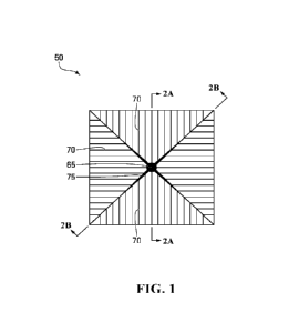
not on the
side exposed to the light source, allowing for a higher conductive cross-
section. In
such a configuration, current passes from the frontside to the backside using
vias
that connect the frontside surface to the backside surface where the
electrical
interconnects are disposed.
SUMMARY
[0003] In accordance with an aspect of the invention, an
apparatus is provided.
The apparatus includes a semiconductor material to absorb energy from a
photon.
The energy is to be converted to a current. The apparatus further includes a
positive
electrode disposed on a backside of the semiconductor material to collect the
current
from the backside. In addition, the apparatus includes a via to connect the
backside
of the semiconductor material electrically to a frontside of the semiconductor
material. The apparatus also includes a plurality of fingers disposed on the
frontside
CA 03215477 2023- 10- 13
WO 2022/219568
PCT/IB2022/053492
2
of the semiconductor material to collect the current from the frontside. Also,
the
apparatus includes a trunkline connected to the plurality of fingers to
deliver the
current to the via. The trunkline increases a cross-sectional area toward the
via to
reduce parasitic resistance.
[0004] A variation of the cross-sectional area may maintain a
substantially
constant current density in the trunkline. The cross-sectional area may vary
as a
non-linear function with distance from the via. In particular, the non-linear
function
may parabolic.
[0005] A finger of the plurality of fingers may increase a
finger cross-sectional
area toward the trunkline to reduce parasitic resistance. In particular, a
variation of
the finger cross-sectional area may maintain a substantially constant current
density
in the finger. The finger cross-sectional area may vary as a finger non-linear
function
with distance from the trunkline along the finger. The finger non-linear
function is
parabolic.
[0006] The plurality of fingers may be disposed in a pattern to
reduce a pathway
distance to the via. The pattern may include each finger of the plurality of
fingers
disposed at an angle relative to the trunkline. In particular, the angle may
be about
45 degrees.
BRIEF DESCRIPTION OF THE DRAWINGS
[0007] Reference will now be made, by way of example only, to
the
accompanying drawings in which:
[0008] Figure 1 is a view of an example of an apparatus to
convert light
energy to electrical energy;
[0009] Figure 2A is a cross-section view of the example
apparatus of figure 1
through the line 2A-2A;
[0010] Figure 2B is a cross-section view of the example
apparatus of figure 1
through the line 2B-2B;
[0011] Figure 3 is a view of a frontside of an example of a
semiconductor
wafer with multiple iterations of the apparatus shown in
figure 1;
[0012] Figure 4 is a view of a frontside of another example
of a
semiconductor wafer with multiple iterations of the apparatus
CA 03215477 2023- 10- 13
WO 2022/219568
PCT/IB2022/053492
3
shown in figure 1;
[0013] Figure 5 is a view of a frontside of another example
of a
semiconductor wafer with multiple iterations of the apparatus
shown in figure 1;
[0014] Figure 6 is a view of another example of an apparatus
to convert light
energy to electrical energy;
[0015] Figure 7 is a view of a frontside of an example of a
semiconductor
wafer with multiple iterations of the apparatus shown in
figure 6;
[0016] Figure 8 is a view of another example of an apparatus
to convert light
energy to electrical energy;
[0017] Figure 9 is a view of a frontside of an example of a
semiconductor
wafer with multiple iterations of the apparatus shown in
figure 8;
[0018] Figure 10 is a view of a frontside of another example
of a
semiconductor wafer with multiple iterations of the apparatus
shown in figure 1 and a break;
[0019] Figure 11 is a view of a frontside of another example
of a
semiconductor wafer with multiple iterations of another
example apparatus with additional connectors;
[0020] Figure 12 is a detailed view of a portion of the
frontside of the example
of a semiconductor wafer shown in figure 11; and
[0021] Figure 13 is a view of another example of an apparatus
to convert light
energy to electrical energy.
DETAILED DESCRIPTION
[0022] In describing the components of the device and
alternative examples of
some of these components, the same reference number may be used for elements
that are the same as, or similar to, elements described in other examples. As
used
herein, any usage of terms that suggest an absolute orientation (e.g. "top",
"bottom",
"front", "back", etc.) are for illustrative convenience. Such terms are not to
be
construed in a limiting sense as it is contemplated that various components
will, in
practice, be utilized in orientations that are the same as, or different than
those
described or shown.
CA 03215477 2023- 10- 13
WO 2022/219568
PCT/IB2022/053492
4
[0023] Emitter wrap through and metal wrap through photovoltaic
cells with back
contacts are known. In general, the emitter wrap through and metal wrap
through
photovoltaic cells are built on the engine of both n-type and p-type mono-
crystalline
silicon (c-Si) solar cells using designs prior to PERC (passivated emitter
rear
contact) and SE (selective emitter) technologies. The design of the frontside
metallization patterns are limited only by screen printing technologies which
may be
fairly complex in order to efficiently deliver the photocurrent from all the
areas of the
photovoltaic cell to the vias where the emitter is wrapped through to the
backside of
the cell. These types of designs may feature leaf-like veins radially
emanating
outward from the vias.
[0024] As the solar cell engine transitioned to a PERC design in
combination with
more complex LDSE (laser-doped selective emitter) processes, there are
fundamental limitations in the complexity of the frontside metallization
pattern that
the laser tools can achieve to properly dope and align the emitter regions to
the
frontside metallization. As a result, metal wrap through designs have been
aesthetically lackluster and more non-optimized for efficient transport of
generated
current to the vias.
[0025] An apparatus is provided to reduce a current density
bottleneck that may
occur as the frontside metallization pattern delivers current to the vias. As
more
current is added to the metallization pattern, it is to be appreciated by a
person of
skill in the art with the benefit of this description, that the current
density being
carried by the finger or trunkline increases. The increased current density
may lead
to an increase of the overall parasitic resistance as the current moves closer
to the
vias. Accordingly, the apparatus addresses this issue by using a frontside
metallization pattern that decreases the length of the current pathway from a
frontside location. In addition, the frontside metallization pattern may vary
the cross-
sectional area of the pattern of the trunklines and/or fingers, such as by a
parabolic
or other non-linear function, to maintain a substantially constant current
density from
regions further from the via to regions proximate to the via. By reducing the
variation
of the current density, parasitic resistive losses are reduced. In some
examples, the
variation of the cross-sectional can be designed without increasing the
percentage of
the solar cell which is shaded by the metallization to increase cell
efficiency without
consuming more paste. Likewise, fingers/trunklines can be made taller and
narrower
(matching cross-sectional area) to further decrease shading losses without
CA 03215477 2023- 10- 13
WO 2022/219568
PCT/IB2022/053492
compromising the substantially constant current density toward the vias.
[0026] Referring to figures 1, 2A, and 2B, a representation of
an apparatus to
convert light energy to electrical energy is generally shown at 50. The
apparatus 50
may be part of a larger cell with a plurality of vias 65 to convert light
energy. The
present example shows a single unit which may be replicated across a
semiconductor wafer, such as shown in figure 3. The apparatus 50 includes a
semiconductor material 55, a positive electrode 60, a via 65, a plurality of
fingers 70
and a trunkline 75.
[0027] The semiconductor material 55 is not particularly limited
and may be any
material capable of converting light energy to electrical energy. For example,
the
semiconductor material 55 may be silicon, such as a p-type mono-crystalline
silicon
doped with gallium or boron or n-type mono-crystalline silicon doped with
phosphorus.
[0028] The semiconductor material 55 is to absorb energy from an
incoming
photon and convert the energy to electrical energy in the form a current
through a
closed circuit from the positive electrode 60 to the frontside of the
semiconductor
material 55. In the present example, the semiconductor material 55 is a
photovoltaic
cell where an electric current is generated via the photoelectric effect. The
current is
collected by the positive electrode 60 on the backside of the semiconductor
material
55 and from the frontside of the semiconductor material 55 via the plurality
of fingers
and the trunklines 75. In the present example, the apparatus shown at 50 may
provide a voltage between the frontside and backside of about 0.675 volts and
be
able to generate a current density of about 41 mA/cm2.
[0029] In the present example, the positive electrode 60 is
disposed on the
backside of the semiconductor material 55. The positive electrode 60 is to
collect
the current from the backside of the semiconductor material 55. In some
examples,
the positive electrode 60 may also serve as a positive contact pad in the
electrical
circuit.
[0030] The via 65 is a hole through the semiconductor material
55 to allow the
backside of the semiconductor material 55 to connect to the frontside.
Accordingly,
the via 65 provides for the negative electrode disposed on the frontside the
of
semiconductor material 55 to connect with the electrical circuit using
contacts
disposed on the backside. The manner by which the via 65 is formed is not
limited.
In the present example, a wafer may be drilled as an initial processing steps
using a
CA 03215477 2023- 10- 13
WO 2022/219568
PCT/IB2022/053492
6
laser. The hole may then be filled with a metallic paste as one of the final
processing
steps to form the via 65.
[0031] The negative electrode disposed on the frontside of the
semiconductor
material is not particularly limited and may include various patterns. The
negative
electrode is to contact the frontside surface of semiconductor material 55 to
collect
current for the electrical circuit. Since photons are to be absorbed by the
frontside of
the semiconductor material 55, it is to be appreciated by a person of skill
with the
benefit of this description that the negative electrode is to be designed to
allow for as
much light to pass through as possible. Since the negative electrode is
generally
made from a non-transparent metal, such as silver, it is to be appreciated
that the
footprint of the negative electrode is to be reduced to allow more photons to
pass
through to the semiconductor material 55. However, by reducing the footprint
of the
negative electrode, the current density increases, which results in the
increase of
parasitic resistance in the electrical circuit.
[0032] In the present example, the negative electrode includes a
plurality of
fingers 70 and at least one trunkline 75. The plurality of fingers 70 are to
collect
current from different portions of the frontside of the semiconductor material
55. The
plurality of fingers 70 are fine lines of conductive material, such as silver,
to allow for
as much light to pass around them as possible where the light is to be
converted to
electrical energy collected by the fingers 70. Current generated in portions
of the
semiconductor material 55 proximate to a finger 70 are carried to a trunkline
75
which is electrically connected to multiple fingers 70. Accordingly, the
trunkline 75
collects current from an area of the frontside of the semiconductor material
55 and
carries the current to the via 65 where the current is transferred to the
backside of
the semiconductor material 55 through the via 65. The positive electrode 60
and the
negative electrode (through the via 65) may then be connected to form the
electrical
circuit at the backside of the semiconductor material 55.
[0033] In the present example, the trunkline 75 includes a
varying structure to
maintain the current density as more current is collected from additional
fingers 70
along the length of the trunkline 75 toward the via 65. In particular, the
trunkline 75
increases its cross sectional area closer to the via 65. The manner which the
trunkline 75 varies is not particularly limited. For example, the width of the
trunkline
75 may decrease as a function of distance from the via 65 as shown in figure
1. In
addition, the height of the trunkline 75 may decrease as a function of
distance from
CA 03215477 2023- 10- 13
WO 2022/219568
PCT/IB2022/053492
7
the via 65 as shown in figure 2B. By increasing the cross sectional area of
the
trunkline 75 closer to the via 65, additional current added to the trunkline
75 from
fingers 70 will be offset by the increase in cross sectional area such that
the current
density remains substantially constant. By maintaining the current density
along the
length of the trunkline 75, bottlenecks caused by an increase in parasitic
resistance
in the electrical pathway is reduced.
[0034] It is to be appreciated by a person of skill with the
benefit of this
description that the variation of the cross section area of the trunkline 75
as a
function of distance from the via 65 is not particularly limited. In
particular, the
current density in the trunkline 75 may be dependent on the pattern of the
fingers 70
and the amount of current each finger 70 adds to the trunkline 75. For
example, the
variation of the cross section of the trunkline 75 as a function of distance
from the via
65 may be non-linear. In some examples, the function may be a parabolic
function.
[0035] In the present example, the pattern of the negative
electrode is designed
as shown in figure 1 to reduce the pathway distance to the via 65 from any
point on
the frontside of the semiconductor material 55. In particular, the plurality
of fingers
70 may be oriented at an angle relative to a respective trunkline 75, such as
about
45 degrees. Furthermore, the size of the apparatus 50 is not particularly
limited and
may be dimensioned to fit as a unit of a repeating pattern on a wafer of any
size.
[0036] Referring to figure 3, a solar cell 100 to convert light
energy to electrical
energy is shown. In the present example, the solar cell 100 includes a
plurality of
apparatuses 50, which are repeating units of the solar cell 100. The size of
the solar
cell 100 is not particularly limited. For example, the solar cell 100 may be
formed
with 36 apparatuses 50 arranged in a 6x6 grid pattern on a full square or
pseudo-
square 158.75mm wafer.
[0037] Referring to figure 4, another solar cell 200 to convert
light energy to
electrical energy is shown. In the present example, the solar cell 200
includes a
plurality of apparatuses 50, which are repeating units of the solar cell 200.
The size
of the solar cell 200 is not particularly limited. For example, the solar cell
200 may
be formed with 64 apparatuses 50 arranged in an 8x8 grid pattern on a full
square or
pseudo-square 166mm wafer.
[0038] Referring to figure 5, another solar cell 200a to convert
light energy to
electrical energy is shown. In the present example, the solar cell 200a
includes a
plurality of apparatuses 50, which are repeating units of the solar cell 200a.
The size
CA 03215477 2023- 10- 13
WO 2022/219568
PCT/IB2022/053492
8
of the solar cell 200a is not particularly limited. For example, the solar
cell 200a may
be formed with 36 apparatuses 50 arranged in an 6x6 grid pattern on a full
square or
pseudo-square 166mm wafer.
[0039] Referring to figure 6, another example of an apparatus
50b to convert light
energy to electrical energy is shown. Like components of the apparatus 50b
bear
like reference to their counterparts in the apparatus 50, except followed by
the suffix
"b". The apparatus 50b may be part of a larger cell with a plurality of vias
65b to
convert light energy. The apparatus 50b includes a semiconductor material 55b,
a
positive electrode (not shown), a via 65b, a plurality of fingers 70b and a
trunkline
75b.
[0040] In this example, the fingers 70b are perpendicular the
trunkline 75b. As
illustrated, the width of the trunkline 75b increases based on the number of
fingers
70b that feed into the trunkline 75b as a function of the distance from the
via 65b. In
this example, it is to be appreciated that each finger 70b is to collect a
substantially
equivalent amount of current. Accordingly, since the current added to the
trunkline
75b increases in a substantially linear manner toward the via 65b, it is to be
appreciated by a person of skill with the benefit of this description that the
variation
of the cross section of the trunkline 75b as a function of distance from the
via 65b
may be linear.
[0041] Referring to figure 7, a solar cell 200b to convert light
energy to electrical
energy is shown. In the present example, the solar cell 200b includes a
plurality of
apparatuses 50b, which are repeating units of the solar cell 200b. The size of
the
solar cell 200b is not particularly limited. For example, the solar cell 200b
may be
formed with 36 apparatuses 50b arranged in a 6x6 grid pattern on a full square
or
pseudo-square 166mm wafer.
[0042] Referring to figure 8, another example of an apparatus
50c to convert light
energy to electrical energy is shown. Like components of the apparatus 50c
bear
like reference to their counterparts in the apparatus 50, except followed by
the suffix
"c". The apparatus 50c may be part of a larger cell with a plurality of vias
65c to
convert light energy. The apparatus 50c includes a semiconductor material 55c,
a
positive electrode (not shown), a via 65c, a plurality of fingers 70c and a
trunkline
75c.
[0043] In this example, the apparatus 50c is an elongated
version of the
apparatus 50. In this example, the cross section area of the trunkline 75c
varies in a
CA 03215477 2023- 10- 13
WO 2022/219568
PCT/IB2022/053492
9
manner that is not particularly limited. For example, the width of the
trunkline 75c
may decrease as a function of distance from the via 65. Alternatively, or in
combination with varying the width, the height of the trunkline 75c may
decrease as
a function of distance from the via 65c. By increasing the cross sectional
area of the
trunkline 75c closer to the via 65c, additional current added to the trunkline
75c from
fingers 70c will be offset by the increase in cross sectional area such that
the current
density remains substantially constant.
[0044] It is to be appreciated by a person of skill with the
benefit of this
description that the variation of the cross section area of the trunkline 75b
as a
function of distance from the via 65b is not particularly limited. In
particular, the
current density in the trunkline 75b may be dependent on the pattern of the
fingers
70b and the amount of current each finger 70b adds to the trunkline 75b. For
example, the variation of the cross section of the trunkline 75b as a function
of
distance from the via 65b may be a parabolic function.
[0045] Referring to figure 9, another solar cell 200c to convert
light energy to
electrical energy is shown. In the present example, the solar cell 200c
includes a
plurality of apparatuses 50c, which are repeating units of the solar cell
200c. The
size of the solar cell 200c is not particularly limited. For example, the
solar cell 200c
may be formed with 48 apparatuses 50 arranged in a 6x8 grid pattern on a full
square or pseudo-square 166mm wafer.
[0046] Referring to figure 10, an example of solar cells 200d-1
and 200d-2
(generically, these solar cells are referred to herein as "solar cells 200d"
and
collectively they are referred to as "solar cells 200c1") to convert light
energy to
electrical energy are shown. In the present example, the solar cells 200d may
include a plurality of apparatuses 50, which are repeating units on each solar
cell
200d. The size of the solar cells 200d are not particularly limited. For
example, the
solar cells 200d may be formed on a full square or pseudo-square 166mm wafer.
In
the present example, the solar cell 200d-1 includes 12 apparatuses 50 arranged
and
six apparatuses 251 disposed along the gap 210d. The solar cell 200d-2 is
substantially a mirror image of the solar cell 200d-1 and includes 12
apparatuses 50
arranged and six apparatuses 252 disposed along the gap 210d. The manner by
which the solar cells 200d are formed is not particularly limited. In the
present
example, a pattern of 36 apparatuses 50 arranged in a 6x6 grid pattern on a
full
square or pseudo-square wafer may be screen printed through mask having an
CA 03215477 2023- 10- 13
WO 2022/219568
PCT/IB2022/053492
additional break in the center of the solar cell. The screen print mask is
subsequently removed to form the gap 210d and an electrical break between the
solar cells 200d. Accordingly, the apparatuses 251 and the apparatuses 252
along
the gap 210d are asymmetrical. The width of the gap 210d is not particularly
limited.
In the present example, the gap 210d is about 2mm. However, in other examples,
the gap 210d may be wider or narrower.
[0047] It is to be appreciated by a person of skill with the
benefit of this
description that the gap 210d may be provided to accommodate cutting to
separate
the solar cells 200d. The cutting line is to be along the gap 210 where no
fingers or
gridlines are present. This facilitates cutting by allowing for a laser or
another cutting
process to occur without obstruction to provide for a cleaner cut.
[0048] Referring to figure 11, another example of solar cells
200e-1 and 200e-2
(generically, these solar cells are referred to herein as "solar cells 200e"
and
collectively they are referred to as "solar cells 200e") to convert light
energy to
electrical energy are shown. Like components of the solar cells 200d bear like
reference to their counterparts in the solar cells 200d, except followed by
the suffix
"e". For example, the solar cells 200d are separated by a gap 210e.
[0049] Referring to figure 12, a portion 250e of the solar cells
200e are shown in
greater detail. In the present example, the portion 250e a repeating unit and
the
surrounding area of each repeating unit. The portion 250e includes a
semiconductor
material 55e, a positive electrode (not shown), a via 65e, a plurality of
fingers 70e, a
connector 72e, and a trunkline 75e.
[0050] In the present example, the repeating unit is
substantially the same as the
apparatus 50 with the addition of the connectors 72e. It is to be appreciated
by a
person of skill with the benefit of this description that the connectors 72e
increased
the redundancy of the solar cell 200e by connecting adjacent fingers 70e. In
particular, the connectors 72e reduce the impact of manufacturing defects in
the
metallization, such as small gaps, by providing alternative pathways for the
current
collected from the frontside of the semiconductor material 55e to reach the
trunkline
75e. The placement of the connectors 72e as well as the number of connectors
72e
disposed on the semiconductor material 55 is not particularly limited. It is
to be
appreciated by a person of skill with the benefit of this description that
additional
connectors 72e will provide additional redundancy against defects. However,
each
additional connector 72e will increase the shading of the semiconductor
material
CA 03215477 2023- 10- 13
WO 2022/219568
PCT/IB2022/053492
11
55e.
[0051] Referring to figure 13, another example of an apparatus
50f to convert light
energy to electrical energy is shown. Like components of the apparatus 50f
bear like
reference to their counterparts in the apparatus 50, except followed by the
suffix "f".
The apparatus 50f may be part of a larger cell with a plurality of vias 65f to
convert
light energy. The apparatus 50f includes a semiconductor material 55f, a
positive
electrode (not shown), a via 65f, a plurality of fingers 70f and a trunkline
75f.
[0052] In this example, the apparatus 50f includes fingers 70f
that are tapered to
increase the cross section area of the finger 70f as it approaches the
trunkline 75f.
The manner by which the fingers 70f taper is not particularly limited. The
tapering
away from the trunkline 75f results in an increase in the width of the finger
70f as it
approaches the trunkline 75f. In the present example, the height of the finger
70f
above the semiconductor material 55f is substantially constant. Accordingly,
the
increase in width approaching the trunkline 75f will result in an increase in
cross
section area of the finger 70f. Since the current added to the finger 70f
increases in a
substantially linear manner toward the trunkline 75f, the corresponding
increase in
the cross section area of the finger 70f closer to the trunkline 75f maintains
a current
density throughout the length of the finger 70f that is substantially constant
to reduce
the parasitic resistance within each finger 70f.
[0053] It is to be understood that variations are contemplated.
For example, the
apparatus 50 is not particularly limited in size and may have various
dimensions to fit
a targeted number of units on a wafer of any size. When varying the size of
the
apparatus 50, additional fingers 70 may be added to each apparatus 50 to
provide
effective collection of current from the frontside of the semiconductor
material 55. As
another example of a variation, it is to be appreciated by a person of skill
that each
wafer may have a combination of different apparatuses, such as a mixture of
apparatus 50 and apparatus 50b.
[0054] Various advantages will become apparent to a person of
skill in the art with
the benefit of this description. For example, the metallization pattern of the
negative
electrode show in the various examples may be used improve performance without
resorting to other means such as by using more costly materials to reduce
parasitic
resistance, such as silver, or by adding more vias, which introduces a
significant cost
such as reduced throughput, higher capital expenditure, and additional
potential
points of failure (i.e. more defect sites for shunts or cell cracks).
CA 03215477 2023- 10- 13
WO 2022/219568
PCT/IB2022/053492
12
[0055] It is to be recognized that features and aspects of the
various examples
provided above may be combined into further examples that also fall within the
scope of the present disclosure.
CA 03215477 2023- 10- 13