Note: Descriptions are shown in the official language in which they were submitted.
CA 03217335 2023-10-17
WO 2022/246074 PCT/US2022/030043
SOLID-STATE AMORPHOUS SELENIUM AVALANCHE DETECTOR WITH HOLE
BLOCKING LAYER
STATEMENT REGARDING FEDERALLY SPONSORED RESEARCH
[0001] This invention was made with government support under EB026644 awarded
by National
Institutes of Health and DE-SC0012704 awarded by the Department of Energy. The
government
has certain rights in the invention.
CROSS-REFERENCE TO RELATED APPLICATION
[0002] This application claims the benefit of and priority to U.S. Provisional
Application Serial
No. 63/190,394 filed on May 19, 2021, the entirety of which is incorporated by
reference.
FIELD OF THE DISCLOSURE
[0003] This disclosure relates to solid-state radiation imaging detectors and
methods of
manufacturing the same.
BACKGROUND
[0004] Efficient sensing and imaging of low-light signals down to the single
photon level with a
true solid-state photomultiplier has been a long-standing quest with a wide
range of applications
in astronomy and spectroscopy, medical imaging, and the rapidly developing
field of quantum
optics and quantum information science. Low-light detection technology, which
utilizes the
avalanche phenomena for increasing the signal-to-noise ratio (SNR), is an
extremely powerful
tool that enables a deeper understanding of more sophisticated phenomena. The
measurement
under light-starved conditions offers the following unique advantages:
nondestructive analysis of
a substance, high-speed time-of-flight properties, and single-photon
detectability.
[0005] One known commercial detector for low-light detection with high dynamic
range and
linear mode operation is the vacuum photo multiplier tube (PMT). Although the
main advantage
of PMTs is high gain (typically 105-108) with low excess noise and room
temperature operation,
they are bulky and fragile, have poor quantum efficiency in the visible
spectrum, are insensitive
to infrared light and highly sensitive to magnetic fields. In comparison, key
advantages of solid-
state technology are ruggedness, compact size, insensitivity to magnetic
fields, and excellent
1
CA 03217335 2023-10-17
WO 2022/246074 PCT/US2022/030043
uniformity of response. In practical avalanche detectors, however, the amount
of enhancement in
SNR is often severely limited by excess noise caused by the stochastic nature
of the avalanche
impact ionization process and the optimal SNR typically occurs at very low
gain values.
[0006] Another known detector uses amorphous selenium (a-Se) as a bulk
avalanche i-layer.
Amorphous Selenium (a-Se) based solid-state detectors have some very distinct
advantages. For
example, a-Se is readily produced uniformly over a larger area at
substantially lower costs, as
compared to crystalline semiconductors. Additionally, a-Se is the only
amorphous material that
produces impact ionization avalanche gain at high fields and is the only
exception to the Webb's
criterion because only holes become hot carriers and undergo avalanche
multiplication, and
consequently, avalanche selenium devices are linear-mode devices with a
negligibly small excess
noise. a-Se has been used in optical cameras. For example, the avalanche gain
in a-Se enabled
the development of the first optical camera with more sensitivity than human
vision and, for
example, capable of capturing astronomical phenomena such as auroras and solar
eclipses.
[0007] a-Se also has a wide bandgap (2.1 eV) room-temperature semiconductor
with ultra-low
thermal generation of carriers even at high fields. Moreover, the a-Se layer
can be deposited over
thin-film-transistors (TFT) in the read-out electronics at temperatures that
would not damage the
underlying active-matrix readouts (below - 200 C).
[0008] However, even with all of these advantageous, the development of solid-
state avalanche
a-Se devices with a 2D-array of pixelated readout (detector) has been
difficult to achieve,
especially due to an inefficient hole blocking layer(s). For example, at
substantially high electric
fields required for impact ionization, an optimized termination is required to
reach stable
blocking with minimum dark or leakage currents. Moreover, it is a
technological challenge to
avoid possible dielectric breakdown of the detector when the electric field
experiences local
enhancement at the hole blocking layer/high-voltage-metal-electrode interface,
thus leading to
enhanced hole injection from the high voltage electrode. This uncontrolled
injection causes a
high current flow that can induce a phase transition due to Joule heating,
thus leading to
crystallization in the a-Se layer. This crystallization results in a drop of
resistivity, enabling an
even higher current flow in the a-Se layer, which further increases Joule
heating, resulting in a
runaway effect which ultimately leads to a dielectric breakdown of the device.
2
CA 03217335 2023-10-17
WO 2022/246074 PCT/US2022/030043
SUMMARY
[0009] Accordingly, disclosed is a photomultiplier which comprises a first
electrode, a hole
blocking layer (HBL), a photoconductive layer, an electron blocking layer
(EBL) and a second
electrode. The photoconductive layer may comprise amorphous selenium (a-Se).
The HBL may
comprises a n-type material having a dielectric constant of at least 50. The
EBL may comprise a
p-type material. The a-Se photoconductive layer may be between the EBL and the
HBL. The
HBL may be between the first electrode and the a-Se layer. The EBL may be
between the second
electrode and the a-Se layer.
[0010] In an aspect of the disclosure, the dielectric constant of the n-type
material may be
between about 50 and about 3000. For example, the n-type material may be
selected from a
group consisting of Barium Titanate, Strontium Titanate, Barium Strontium
Titanate, and
Titanium Oxide. In some aspects, the n-type material may be Strontium Titanate
(SrTiO3)
("STO"). The STO may be formed as a single crystal or thin film. The single
crystal may have a
dielectric constant of about 300.
[0011] In an aspect of the disclosure, the photomultiplier may have an
avalanche gain about 150
at an applied bias of about 3750 V.
[0012] In an aspect of the disclosure, the HBL may have a thickness of about
50 nm to 1
[0013] In an aspect of the disclosure, the a-Se layer may have a thickness
between about 50 nm
and about 35 tm, inclusive. The thickness may be based on an application.
[0014] In an aspect of the disclosure, the p-type material may have a
dielectric constant of at
least 50. For example, the p-type material may be Ni02
[0015] In an aspect of the disclosure, the first electrode may be transparent.
For example, the
first electrode may be made of indium tin oxide (ITO).
[0016] In an aspect of the disclosure, the photomultiplier may further
comprise a readout device.
[0017] Also disclosed is a photomultiplier which comprises a first electrode,
a hole blocking
layer (HBL), a photoconductive layer, an electron blocking layer (EBL) and a
second electrode.
The photoconductive layer may comprise amorphous selenium (a-Se). The HBL may
comprises
Strontium Titanate (SrTiO3) ("STO"). The EBL may comprise a p-type material.
The a-Se
photoconductive layer may be between the EBL and the HBL. The HBL may be
between the
first electrode and the a-Se layer. The EBL may be between the second
electrode and the a-Se
layer.
3
CA 03217335 2023-10-17
WO 2022/246074 PCT/US2022/030043
[0018] In an aspect of the disclosure, the STO may be formed as a single
crystal or thin film. The
single crystal may have a dielectric constant of about 300.
[0019] In an aspect of the disclosure, the photomultiplier may have an
avalanche gain about 150
at an applied bias of about 3750 V.
[0020] In an aspect of the disclosure, the p-type material may be Ni02.
[0021] Also disclosed is a method of manufacturing a photomultiplier. The
method may
comprise fabricating a first part of the photomultiplier, fabricating a second
part of the
photomultiplier and combining the first part and the second part.
[0022] The fabrication of the first part may comprise depositing an electron
blocking layer
comprising a p-type material on a readout device; and depositing a first
portion of a-Se
photoconductive layer having a first thickness of the electron blocking layer.
[0023] The fabrication of the second part may comprise depositing a hole
blocking layer
comprising a n-type material having a dielectric constant of at least 50 on a
substrate; and
depositing a second portion of a-Se photoconductive layer having a second
thickness on the hole
blocking layer. The substrate may comprise an electrode.
[0024] The combining may comprise heating the first part and the second part
to at least a glass
transition temperature of the a-Se photoconductive layer; and applying
pressure to fuse the first
portion of the a-Se photoconductive layer and the second portion of the a-Se
photoconductive
layer thereby combining the first part and the second part.
[0025] Another electrode may be formed on a readout device.
[0026] In an aspect of the disclosure, the first thickness may be the same as
the second thickness.
[0027] In an aspect of the disclosure, the n-type material is selected from a
group consisting of
Barium Titanate, Strontium Titanate, Barium Strontium Titanate, and Titanium
Oxide. For
example, the n-type material may Strontium Titanate (SrTiO3) ("STO").
[0028] In an aspect of the disclosure, the electron blocking layer may
comprise Ni02.
[0029] Also disclosed is another method of manufacturing a photomultiplier.
The method may
comprise depositing an electron blocking layer comprising a p-type material on
a readout device
where the readout device has a common electrode, thermally deposit a-Se layer
on the electron
blocking layer, depositing at a temperature less than a glass transition
temperature of the a-Se
layer, hole blocking layer comprising a n-type material having a dielectric
constant of at least 50
and depositing another electrode on the hole blocking layer.
4
CA 03217335 2023-10-17
WO 2022/246074 PCT/US2022/030043
[0030] In an aspect of the disclosure, the hole blocking layer is deposited
using RF sputtering.
[0031] In an aspect of the disclosure, the n-type material is selected from a
group consisting of
Barium Titanate, Strontium Titanate, Barium Strontium Titanate, and Titanium
Oxide. For
example, the n-type material may Strontium Titanate (SrTiO3) ("STO").
[0032] In an aspect of the disclosure, the electron blocking layer may
comprise Ni02.
BRIEF DESCRIPTION OF THE DRAWINGS
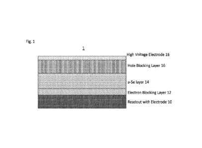
[0033] Fig. 1 illustrates an example of a solid-state amorphous selenium
avalanche detector
("avalanche detector") in accordance with aspects of the disclosure;
[0034] Fig. 2 illustrates an example of a method of fabricating an avalanche
detector in
accordance with aspects of the disclosure;
[0035] Fig. 3A illustrates an example of a method of fabricating the first
part of the avalanche
detector in accordance with aspects of the disclosure;
[0036] Fig. 3B illustrates an exploded view of a representation of the first
part of the avalanche
detector in accordance with aspects of the disclosure;
[0037] Fig. 4A illustrates an example of a method of fabricating the second
part of the avalanche
detector in accordance with aspects of the disclosure;
[0038] Fig. 4B illustrates an exploded view of a representation of the second
part of the
avalanche detector in accordance with aspects of the disclosure;
[0039] Fig. 5A illustrates an example of a method of combining the first part
and the second part
of the avalanche detector in accordance with aspects of the disclosure;
[0040] Fig. 5B illustrates an exploded view of a representation of the
avalanche detector
showing both portions of the a-Se layer in accordance with aspects of the
disclosure;
[0041] Fig. 6A illustrates another example of a method of fabricating the
avalanche detector in
accordance with aspects of the disclosure;
[0042] Fig. 6B illustrates an exploded view of a representation of the
avalanche detector
fabricated as shown in Fig. 6A in accordance with aspects of the disclosure;
[0043] Fig. 7 illustrates a step-by-step process of fabricating a test
detector in accordance with
aspects of the disclosure, where the test detector is a planar n-i detector;
[0044] Fig. 8 illustrates a schematic of the test detector in accordance with
aspects of the
disclosure;
CA 03217335 2023-10-17
WO 2022/246074 PCT/US2022/030043
[0045] Fig. 9 illustrates the test detector under testing (DUT);
[0046] Fig. 10 illustrates the measurement results of an avalanche gain as a
function of the
applied bias voltage in accordance with aspects of the disclosure;
[0047] Fig. 11 illustrates the measurement results of a dark current density
as a function of the
applied bias voltage in accordance with aspects of the disclosure;
[0048] Fig. 12 illustrates simulation and measurement results of excess noise
factor of a detector
in accordance with aspects of the disclosure and comparison with other
devices;
[0049] Fig. 13 illustrates measured and predicted effective quantum efficiency
verses electric
field;
[0050] Fig. 14 illustrates simulation results showing a comparison of the
electric field in the i-
layer from different n-layers;
[0051] Fig. 15 illustrates a simulated energy band diagram for a detector in
accordance with
aspects of the disclosure;
[0052] Fig. 16 illustrates a simulated electric field in the HBL versus the a-
Se layer in
accordance with aspects of the disclosure;
[0053] Fig. 17 illustrates a simulated electric field as a function of the
applied bias in accordance
with aspects of the disclosure; and
[0054] Fig. 18 illustrates a simulated energy band diagram for another
detector in accordance
with aspects of the disclosure with both p and n blocking layers.
DETAILED DESCRIPTION
[0055] In accordance with aspects of the disclosure, a solid-state avalanche
detector has a high-
lc dielectric hole-blocking layer (HBL). For purposes of the describes, "high-
lc dielectric" means
a dielectric greater than 50. The "high- lc dielectric" also refers to a
dielectric less than 3000.
Advantageously, the HBL as described herein decreases the electric field at
the HBL/high-
voltage metal electrode interface which limits Schottky injection from the
high voltage electrode,
which in turn prevents Joule heating from crystalizing an a-Se layer (bulk
layer). This avoids the
runaway effect. The HBL as described herein also avoids early dielectric
breakdown on the
detector, which may enable achieving avalanche gains equal to the theoretical
gain of the a-Se
layer and comparable to vacuum PMTs (on the order of 106). Thus, the HBL as
described herein
6
CA 03217335 2023-10-17
WO 2022/246074 PCT/US2022/030043
enables the solid-state avalanche detector to be reliable and have a
repeatable impact ionization
gain with the irreversible breakdown.
[0056] Fig. 1 illustrates a solid-state amorphous selenium avalanche detector
1 in accordance
with aspects of the disclosure (avalanche detector 1). The avalanche detector
1 comprises a
readout 10 (also referred to as "ROTC" or "readout device". In an aspect of
the disclosure, the
readout 10 may comprise the common electrode as shown in Fig. 1. However, in
other aspects,
the common electrode may be separate and deposited on the readout in a known
manner. In an
aspect of the disclosure, the common electrode may have a thickness about 20
nm to about 200
nm.
[0057] The readout 10, may either be used for photon counting (CMOS substrate)
or energy
integration (CMOS or TFT substrate) applications. A thin-film-transistor (TFT)
substrate or a
complementary metal-oxide-semiconductor (CMOS) substrate can be utilized with
a previously
patterned common/ground electrode to form the readout 10. The common/ground
electrode
is preferably formed of conductive materials that include Aluminum (Al),
Chromium (Cr),
Tungsten (W), Indium tin oxide (ITO), and Zinc oxide (Zn0). The readout 10
further includes
the circuitry to bias a readout (via data switches) and output the signals
representing the counts
(when photon counting). For example, the readout 10 may have data lines Dl-DN.
The data lines
may be coupled to amplifiers. The readout 10 may include a matrix of active
elements, e.g.,
CMOS or TFT (with a storage capacitor). Each pixel has an active area and a
fill factor.
[0058] The readout 10 may output analog signals to an analog to digital
converter ("ADC").
[0059] The avalanche detector 1 also comprises an electron blocking layer 12.
In an aspect of
the disclosure, the electron blocking layer 12 (EBL) may comprise a material
that is a p-type
material (with respect to a-Se). The EBL 12 may have a high- lc dielectric. In
an aspect of the
disclosure, the EBL may be made of Ni02. However, the EBL 12 is not limited to
being made of
Ni02 Other p-type, high- lc dielectric may be used to isolate the a-Se layer
14 from the common
electrode. The EBL 12 blocks or prevents electrons from being injected from
the common
electrode into the a-Se layer 14. The EBL 12 (p-type material) decreases the
electric field at the
EBL/common electrode interface. In an aspect of the disclosure, the EBL 12 may
have a
thickness of about 50 nm to about 1
[0060] The avalanche detector 1 also comprises an a-Se layer 14. The a-Se
layer 14 is a
photoconductive layer. The EBL 12 is between the a-Se layer 14 and the common
electrode (and
7
CA 03217335 2023-10-17
WO 2022/246074 PCT/US2022/030043
readout 10). The thickness of the a-Se layer 14 may depend on the application.
For example, the
a-Se layer 14 may have a thickness of about 500 nm to about 35 iim. Selenium
has a
permittivity of 6.
[0061] The avalanche detector 1 also comprises the HBL 16. As described above,
the HBL 16
reduces an electric field at the HBL/high-voltage electrode interface (hole
injecting interface).
The higher the dielectric of the HBL 16 is, the more the electric field is
reduced. In an aspect of
the disclosure, the HBL 16 may be made of a material that is an n-type
material with respect to
the a-Se layer 14. For example, Strontium Titanate (SrTiO3) (also referred to
as STO) may be
used as the n-type material. The lc value for SrTiO3 may depend on how it is
formed. For
example, a single crystal STO may have a lc about 300. However, when the STO
is fabricated as
a thin film, the STO may have a lc value lower. In aspect of the disclosure,
the single crystal STO
may be used in a detector for a single pixel, whereas the thin film may be
used for a detector 1
having an array of pixels. Other materials, such as other n-type perovskite-
type materials may be
used. However, the materials are not limited to perovskites.
[0062] Other materials such as Barium Titanate, Barium Strontium Titanate, and
Titanium Oxide
may be used. Barium Titanate has a reported lc of about 3000. Barium Strontium
Titanate has a
reported lc of about 680. Titanium Oxide has a reported lc up to 70.
[0063] The HBL 16 isolates the a-Se layer 14 from the high voltage electrode
18 (e.g., blocking
the holes from being injected from the high voltage electrode 18 into the a-Se
layer 14).
[0064] Thus, by sandwiching the a-Se layer 14 between the high lc blocking
layers (EBL 12,
HBL 16), the a-Se layer 14 is protected. Similar to the EBL 12, the HBL 16 may
have a
thickness of about 50 nm to about 1 iim.
[0065] The avalanche detector 1 also comprises the high voltage electrode 18
(HVE). In an
aspect of the disclosure, the HVE 18 may be transparent to a target wavelength
band. For
example, the HVE 18 may be formed of indium tin oxide (ITO). The ITO may be
transparent to
wavelengths above 300 nm. However, the HVE 18 is not limited to ITO and other
transparent
materials may be used. For example, indium gallium zinc oxide (IGZO) may be
used. While it
is preferred that the HVE 18 is made from a transparent material to allow
light through, it is not
necessary for the common electrode to be made of a transparent material and
the common
electrode may be any of the conductive materials as mentioned above. Similar
to the common
electrode, the HVE 18 may have a thickness of about 20 nm to about 200 nm.
8
CA 03217335 2023-10-17
WO 2022/246074 PCT/US2022/030043
[0066] Fig. 2 illustrates an example of a method of fabricating an avalanche
detector 1 in
accordance with aspects of the disclosure. In accordance with aspects of the
disclosure, the
avalanche detector 1 may be fabricated in two separate parts (First Part and
Second Part) and
subsequently fused together. At 200, the first part of the detector may be
fabricated. Fig. 3A
illustrates an example of a method of fabricating the first part of the
avalanche detector 1. Fig.
3B illustrates an exploded view of a representation the first part of the
avalanche detector 1. This
method may be used to fabricate the avalanche detector 1 because the glass
transition
temperature of a-Se is relatively low (about 50 C). Any material deposited on
a-Se must be
deposited below 50 C or a-Se will crystalize. This method removes the low
temperature
deposition requirement on a-Se to prevent crystallization. At 300, the EBL 12
may be deposited
on the readout 10 at a first temperature. In an aspect of the disclosure, the
first temperature may
be above 50 C. In this aspect of the disclosure, the common electrode is
included in the readout
10. The common electrode may be deposited via physical vapor deposition.
[0067] At 305, a portion of the a-Se layer 14 is deposited on the EBL layer
12. As shown in Fig.
3B, this portion has a thickness of Ti. In some aspects, Ti may be half of the
target thickness of
the a-Se layer 14. However, the thickness of Ti is not limited to half. In an
aspect of the
disclosure, the a-Se may be thermally deposed via a physical vapor deposition
(PVD). As shown
in Fig. 3B, the first portion has the readout 10, the EBL 12 and a portion Ti
of the a-Se.
[0068] At 205, the second part of the avalanche detector 1 may be fabricated.
Fig. 4A illustrates
an example of a method of fabricating the second part of the avalanche
detector 1. Fig. 4B
illustrates an exploded view of a representation the second part of the
avalanche detector 1.
[0069] At 400, the HVE 18' is formed. In an aspect of the disclosure, a glass
substrate may be
used. The electrode (e.g., ITO) may be RF sputtered to a target thickness. The
target thickness
may be about 20 nm to about 200 nm as described above. At 405, the HBL 16 may
be deposited
by RF sputtering the layer on the glass substrate (having the electrode). The
HBL 16 will be in
contact with the HVE 18'. The HBL 16 may be deposited as a thin film having a
target
thickness.
[0070] In other aspects of the disclosure, 400/405 may be omitted when a
single crystal STO is
used as the HBL 16. The rigidly of the single crystal STO eliminates a need
for the glass
substrate and the HVE 18 may be deposited directly on the STO (as the
substrate).
9
CA 03217335 2023-10-17
WO 2022/246074 PCT/US2022/030043
[0071] At 410, a portion of the a-Se layer 14 is deposited on the HBL layer
16. As shown in Fig.
4B, this portion has a thickness of T2. In some aspects, T2 may be half of the
target thickness of
the a-Se layer 14. However, the thickness of T2 is not limited to half. In an
aspect of the
disclosure, the a-Se may be thermally deposed via a physical vapor deposition
(PVD). As shown
in Fig. 4B, the second portion has the HVE 18', the HBL 16 and a portion T2 of
the a-Se. The
HVE in Fig. 4B is identified as 18' since the glass substrate may be present.
[0072] At 210, the first part and the second part of the avalanche detector 1
may be combined.
Fig. 5A illustrates an example of a method of combining the first part and the
second part of the
avalanche detector 1. At 500, the first part and the second part of the
avalanche detector 1 are
heated to above the glass transition temperature of the a-Se layer 14 (e.g.,
above 50 C). Above
the glass transition temperature, the a-Se become a viscous, rubber-like
adhesive which allows
the first part and the second part to fuse together. At 505, while the first
part and the second part
are heated, pressure is exerted on the first part and the second part to fuse
the two portions of the
a-Se layer (Ti and T2). Fig. 5B shows an exploded view of a representation of
the avalanche
detector 1 having the two parts with Ti/T2. Ti/T2 would be fused together at
505 to form the a-
Se layer 14. The arrows in Fig. 5B represent the fusion of Ti/T2.
[0073] In another aspect of the disclosure, the avalanche detector 1 may be
fabricated without
dividing the same into the first part and the second part and fabricated under
a low temperature
(e.g., below the glass transition temperature). Fig. 6A illustrates another
method of fabricating
the avalanche detector 1 in accordance with aspects of the disclosure. Fig. 6B
illustrates a
representation of the avalanche detector 1 fabricated in accordance with Fig.
6A.
[0074] At 600, the EBL layer 12 is deposited on the readout 10. The readout 10
acts as the
substrate for the EBL layer 12. Once again, the common electrode may be in the
readout 10. At
605, the a-Se layer 14 is deposited on the EBL layer 12 (directly) such that
the a-Se layer 14 is in
direct contact with the EBL layer 12. In an aspect of the disclosure, the a-Se
may be deposited
using PVD to achieve a target thickness. At 610, the HBL layer 16 is directly
deposited on the a-
Se layer 14 using low temperature RF sputtering. The low temperature RF
sputtering (below
about 50 C) prevents crystallization of the a-Se. The RF sputtering may
achieve the target
thickness for the HBL layer 16. At 615, the HVE 18 is deposited on the HBL
layer 16. Fig. 6B
depicted a representation of the deposited EBL layer 12 (on the readout 10),
the a-Se layer 14
(deposited on the EBL layer 12), the HBL layer 16 (deposited on the a-Se layer
14) and the HVE
CA 03217335 2023-10-17
WO 2022/246074 PCT/US2022/030043
18 (deposited on the HBL layer 16). The methods depicted in Figs. 2 and 6A are
examples of the
p-i-n fabrication process (holes travel toward the pixels).
[0075] Measurements and Simulations
[0076] An avalanche detector in accordance with aspects of the disclosure was
fabricated. This
avalanche detector did not have an EBL 12. The avalanche detector was
evaluated for avalanche
gain and dark current density. Fig. 7 illustrates a step-by-step process of
fabricating the test
avalanche detector ("test detector") in accordance with aspects of the
disclosure.
[0077] The test detector 800 started as single crystal STO 700. The STO 700
had a lc of 300 and
an optical bandgap of 3.3eV. The STO 700 had a thickness of 500 iim. A Cr
metal layer (HVE
705) was deposited on the STO 700 using DC sputtering. The thickness was 200
nm. On the
other side of the STO, the a-Se layer 710 was deposited by thermally
evaporating 99.99% pure
selenium pellets under a vacuum (2 x 10⁻⁶ Torr at 50 C). The a-Se layer was 8
iim thick. The
ground electrode 715 was fabricated by DC sputtering onto the thermally
deposited a-Se layer
710. The thickness was 200 nm. Cr was used as the ground/command electrode.
[0078] Fig. 8 illustrates a schematic of the test detector 800. Fig. 9
illustrates a test sample for
the detector (DUT). The test sample 800 was fabricated on a sample support 910
for stability.
Also, during testing, the test sample 800 was rested on a stabilizing foam
915. The wires 905
were attached to the respective electrodes using an epoxy 900. In the view in
Fig. 9, the HVE
electrode is hidden, however, the wire 905 connected to the electrode is
shown. Fig. 9 shows the
a-Se 710 sandwiched between the Ground/Common Electrode 715 and the STO 700.
Tape was
used to hold the test sample 800 together. The effective quantum efficiency
(gain) and
dark/leakage current was measurement over a wide range of bias conditions. The
bias voltage
was varied from 500 V to 3750V. Fig. 10 illustrates the measurement results of
the avalanche
gain as a function of the applied bias voltage. The applied bias voltage is on
the x-axis and the
avalanche gain, M is on the y-axis. The use of the STO (with the high lc of
300) enables a gain of
about 150 at 3750 V for the 8 iim a-Se layer 710. Carriers in the a-Se layer
710 get hot at high
electric fields and produce single-carrier impact ionization avalanche,
resulting in enhanced
effective quantum efficiency.
[0079] Different layers thickness may impact the gain.
[0080] Fig. 11 illustrates the measurement results of the dark current density
as a function of the
applied bias voltage. The applied bias voltage is on the x-axis and the dark
current density is on
11
CA 03217335 2023-10-17
WO 2022/246074 PCT/US2022/030043
the y-axis. Beyond 3750 V, the device encountered a soft breakdown localized
and randomly
distributed over the device area.
[0081] Fig. 12 illustrates both measurement results from the test detector 800
and simulate
results for a device having the same properties and thicknesses. The graph
illustrates excess noise
factor (ENF) as a function of avalanche gain, M. The measurements were done at
room
temperature (RF). The measurements 1205 are shown with filled in triangles
(4). The noise
spectral density was measured using an SRS 865A lock-in-amplifier operated in
current input
mode. The spectral method was used to calculate the excess noise. The
different avalanche gains
were obtained by varying the bias voltage (and electric field). The hole-only,
history dependent
(non-Markovian), room temperature impact ionization process is represented by
the filled in
triangles. The measured ENF was between about 1.7 and about 1.9. The
fluctuations in the
avalanche gain (ENF) get progressively worse as the multiplication factor is
increased in the
avalanche photodiodes (APDs) by raising the electric field. The ideal non-
Markov device ENF of
1 is denoted by the line 1200.
[0082] According to McIntyre theory, the slope of the gain versus ENF is a
strong function of
the ratio of two carriers (holes and electrons) ionization rate k where 0 <k<
1. The curves for
three different k values are shown in Fig. 12 (curve 1211 k=0, curve 1212
k=0.01 and curve 1213
k=1). The measured excess noise in test detector 800 is because of the single
carrier non-Markov
branching of hot holes (due to many photon scattering events before a
successfully non-ballistic
impact ionization event).
[0083] Triangles 1210 represent a calculated ENF of 250,000 Monte Carlo hole
trajectories
(simulated). The measured ENF matches closely with the simulated results.
[0084] Fig. 13 illustrates a comparison between detectors having different
HBL. Two detectors
were fabricated having different lc for the HBL. The a-Se layer for the two
detectors was 15 iim.
Insulating HBL (5i02) was deposited on the a-Se layer with RF sputtering. 5i02
has a lc value of
4. A non-insulating solution processed Ce02 was deposited on the a-Se layer.
The Ce02 had a lc
value of 28. Measured values are shown in triangles. Both detectors had
avalanche gains at
fields exceeding 80 V/m. The detector with the 5i02 as the HBL had a maximum
avalanche gain
of 10. The maximum measured value from the detector having the Ce02 as the HBL
was about
40. However, theoretical, the maximum from that detector is around 100.
12
CA 03217335 2023-10-17
WO 2022/246074 PCT/US2022/030043
[0085] A fit, using a double exponential, was used to predict the avalanche
gain from the
detector with SrTiO3 as the HBL for the 15 iim a-Se. The avalanche gain in a-
Se is exponential
as a function of higher fields. It is predicted for the 15 iim a-Se that the
avalanche gain for the
detector would be 106 at about 150 V/i.tm. A vertical dashed line represents a
field threshold of
135 V/i.tm. The dotted curve represents the prediction (fit curve).
[0086] Fig. 14 illustrates simulated detector and simulation results for three
different detectors
have the different HBL (n-layer) (e.g., different lc value). The same
different materials (used in
Fig. 13), e.g., 5i02, Ce02 and SrTiO3 were used for the technology computer-
aided design
(TCAD) simulations. n-i detectors were simulated with the top electrode, the n-
layer and the i
layer. For the i-layer in the simulations a-Se was used. In all three
simulations, the electric field
inside the bulk was 100. However, as can be seen from both detectors with the
5i02 and Ce02 as
the HBL, there were significant hot-spots present. For example, when using the
5i02 as the n-
layer (HBL), the electric field hot-spot at the top electrode/HBL interface
was 400 V/i.tm. There
was some improvement using the Ce02 as the HBL, however, there were still hop-
spots over 200
V/i.tm and in fact, above 300 V/i.tm at the top electrode/HBL interface.
[0087] However, using the SrTiO3 in a manner as described herein, the field
hot-spots are
completely erased as expected. The electric field is effectively contained
within the a-Se (i-
layer). Since the electric field is maintained within the a-Se, the electrodes
may be cold to the
touch (i.e., will have a low-filed interface and thus, low injection).
[0088] Fig. 15 illustrates a simulated energy band diagram for an n-i detector
in accordance with
aspects of the disclosure. A simulated bias voltage was applied to the n-i
detector. The i-layer is
a-Se. The n-layer is a hole blocking layer made of SrTiO3. Light absorbed
through a semi-opaque
electrode (Cr) in the a-Se layer leads to the generation of electron-hole
pairs in the i-layer (a-Se).
The electron is excited from a valence to a conduction band, leaving behind a
hole. The applied
bias creates an energy gradient that separates an electron-hole pair. The
holes travel towards a
ground electrode and avalanche in the process. Specifically, the holes travel
across the a-Se and
are collected at the ground electrode (Cr) while the electrons travel across
the single crystal STO
and are collected at the HV electrode (Cr). Fig. 15 illustrates the hopping
(holes are hopping
toward the Cr ground (closer to axis) and electrons are hopping away from the
axis. At high
electric fields, hole transport in a-Se shifts from localized hopping to
extended state band-like
transport. The conduction band and the valance band are shown. The conduction
band within the
13
CA 03217335 2023-10-17
WO 2022/246074 PCT/US2022/030043
STO has an energy of 4.1eV and the valance band within the STO has an energy
of 7.35 eV. The
slope of the bands depends on the applied bias.
[0089] The STO does not hinder the flow of the electrons. The hole injection
barrier was
simulated to be about 0.769V. The election injection barrier was simulated to
be about 1 eV.
[0090] Fig. 16 illustrates the electric filed distribution over the thickness
of the device. In Figs.
15, 16 and 18, the device length is the thickness. The applied bias is 3750 V.
As shown, most of
the electric field is in the a-Se layer which enables the impact ionization
avalanche. Fig. 16 is
consistent with Fig. 14 where the electric field is limited to the a-Se layer
and not in the STO.
[0091] Fig. 17 illustrates the electric field within the a-Se layer as a
function of the applied bias
voltage. The electric field is approximately linear with respect to the
applied bias voltage. The
high-K STO layer enabled the 8 tm thick a-Se i-layer to withstand electric
fields more than 150
V/i.tm. With a a-Se layer of about 15 tm, avalanche gains in the range of 106-
108 can be
achieved at - 150 V/i.tm. as shown in Fig. 13.
[0092] Fig. 18 illustrates a simulated energy band diagram for an n-i-p
detector (simulated) with
an applied bias voltage in accordance with aspects of the disclosure. The i-
layer is a-Se. The n-
layer is a hole blocking layer made of SrTiO3. The p-layer, electron blocking
layer was Ni02
Ni02has a wide band-gap. With a wide-range of tunable carrier concentrations,
Ni02 has been
used in a variety of applications, such as visible-transparent UV
photodetectors, visible-
transparent solar cells, and UV to visible spectrum light-emitting diodes.
Ni02is also transparent.
[0093] The energy band diagram predicts an increase in electron injection
barrier to 2.5eV
(enhanced). The increase helps decrease the electron component of the dark
injection current
even further. Moreover, there is enhancement of charge sensing by avalanche
multiplication as
the device is protected from localized Joule heating effects.
[0094] This prediction also has an increased hole injection barrier to 2.85e
V. The difference in
the hole injection barrier in Fig. 18 versus Fig. 15 is that in Fig. 18, the
model assumes an ideal
and optimized interface between the Cr electrode and the STO. This assumption
was not used in
Fig. 15 (unoptimized interface was used resulting in a smaller simulated
value). The conduction
band and the valence band have different slopes in Figs. 15 and 18. As noted
above, this is
because a different bias was applied in the different simulations.
[0095] In the discussion and claims herein, the term "about" indicates that
the value listed may
be somewhat altered, as long as the alteration does not result in
nonconformance of the process
14
CA 03217335 2023-10-17
WO 2022/246074 PCT/US2022/030043
or device. For example, for some elements the term "about" can refer to a
variation of 0.1%,
for other elements, the term "about" can refer to a variation of 1% or 10%,
or any point
therein. For example, the term about when used for a measurement in mm, may
include +/ 0.1,
0.2, 0.3, etc., where the difference between the stated number may be larger
when the state
number is larger. For example, about 1.5 may include 1.2-1.8, where about 20,
may include 19.0-
21Ø
[0096] Reference herein to any numerical range expressly includes each
numerical value
(including fractional numbers and whole numbers) encompassed by that range. To
illustrate,
reference herein to a range of "at least 50" or "at least about 50" includes
whole numbers of 50,
51, 52, 53, 54, 55, 56, 57, 58, 59, 60, etc., and fractional numbers 50.1,
50.2 50.3, 50.4, 50.5,
50.6, 50.7, 50.8, 50.9, etc. In a further illustration, reference herein to a
range of "less than 50" or
"less than about 50" includes whole numbers 49, 48, 47, 46, 45, 44, 43, 42,
41, 40, etc., and
fractional numbers 49.9, 49.8, 49.7, 49.6, 49.5, 49.4, 49.3, 49.2, 49.1, 49.0,
etc.
[0097] As used herein terms such as "a", "an" and "the" are not intended to
refer to only a
singular entity, but include the general class of which a specific example may
be used for
illustration. As used herein, terms defined in the singular are intended to
include those terms
defined in the plural and vice versa.
[0098] References in the specification to "one aspect", "certain aspects",
"some aspects" or "an
aspect", indicate that the aspect(s) described may include a particular
feature or characteristic,
but every aspect may not necessarily include the particular feature,
structure, or characteristic.
Moreover, such phrases are not necessarily referring to the same aspect.
Further, when a
particular feature, structure, or characteristic is described in connection
with an aspect, it is
submitted that it is within the knowledge of one skilled in the art to affect
such feature, structure,
or characteristic in connection with other aspects whether or not explicitly
described.
[0099] The described aspects and examples of the present disclosure are
intended to be
illustrative rather than restrictive, and are not intended to represent every
aspect or example of
the present disclosure. While the fundamental novel features of the disclosure
as applied to
various specific aspects thereof have been shown, described and pointed out,
it will also be
understood that various omissions, substitutions and changes in the form and
details of the
devices illustrated and in their operation, may be made by those skilled in
the art without
departing from the spirit of the disclosure. For example, it is expressly
intended that all
CA 03217335 2023-10-17
WO 2022/246074 PCT/US2022/030043
combinations of those elements and/or method steps which perform substantially
the same
function in substantially the same way to achieve the same results are within
the scope of the
disclosure. Moreover, it should be recognized that structures and/or elements
and/or method
steps shown and/or described in connection with any disclosed form or aspects
of the disclosure
may be incorporated in any other disclosed or described or suggested form or
aspects as a
general matter of design choice. Further, various modifications and variations
can be made
without departing from the spirit or scope of the disclosure as set forth in
the following claims
both literally and in equivalents recognized in law.
16