Note: Descriptions are shown in the official language in which they were submitted.
WO 2022/243717
PCT/1B2021/000487
Module for integrating into a card body of a smart card, smart card, and
method of
implanting a module into a card body of a smart card
I. Field of Invention
The present invention generally relates to a module for integrating into card
body of a smart
card, to a smart card, and to a method of implanting a module into a card body
of a smart
card.
State of the Art
A typical smart card is a plastic card, the size of a credit card, having a
pattern of metal
contacts imbedded therein. Present smart cards implement an increasing number
of functions
which result from integrating modules into a card body such that advanced
smart cards include
an internal chip, an antenna and possibly one or more sensors and/or display
modules into a
card body of a smart card, such as a biometric sensor, for example, a
fingerprint sensor, and
an electronic display to display a card validation code (CVC) and/or other
information.
With the advancing integration of smart cards into daily life, it is of great
interest in the art to
provide smart cards with improved fabrication processes and reduced
fabrication costs without
affecting the smart card quality. Consequently, it is an aim to constantly
develop appropriate
techniques and materials which allow the lamination of a plurality of foil
layers together with
an equipping of a laminated card body with appropriate contact structures
and/or modules.
Conventionally, modules are integrated into a card body of a smart card in a
process
comprising milling a recess into the card body and implanting a module into
the card body by
accommodating the module in the recess such that contact pads of the module
are brought
into electrical contact with internal contact structures of the card body and
electrically and
mechanically fixing the module to the card body by means of an adhesive
material and/or a
solder material. When using a solder material for the electrical and
mechanical connection of
modules to the card body, the card body, together with the accommodated
module, are
exposed to a thermal soldering step in which solder material provided on
contact pads of at
least one of the internal contact structure of the card body and the module
establishes a
mechanic and electric connection between the module and the card body. The
solder material
may be subjected to a reflow process for forming a solder bump prior to the
soldering step.
Document US 9684863 B2 shows a smart card with an external connector formed of
an
insulating support and a plurality of external metal contact pads arranged on
an external face
of the support. Furthermore, the smart card has a card body having a housing
in which the
CA 03218135 2023- 11- 6
WO 2022/243717
PCT/IB2021/000487
external connector is arranged and an electronic unit and/or an antenna
electrically connected
to a plurality of internal metal contact pads arranged underneath the external
connector and
respectively aligned with the external pads.
Document DE 1020150078 Al shows a fabrication of a smart card, wherein a card
body of
the smart card is provided with a recess for accommodating therein a chip
module. Within the
recess, contact terminals of an antenna structure are exposed for being
brought into contact
with internal contacts of the chip module when accommodating the chip module
within the
recess. Herein, a solder paste is applied on the exposed contact terminals in
the recess before
accommodating the chip module in the recess. An electrical contact between the
chip module
and the card body is established after locally heating the solder paste.
Document WO 2020/212661 Al discloses a method for manufacturing a biometric
sensor
module for a smart card, wherein a biometric sensor is attached at a rear face
for fingerprint
detection. On the rear face of the biometric sensor module, at least one
connection pad is
provided, the connection pad comprising a zone that is wettable by a welding
material. The
connection pads of the biometric sensor module are brought into electrical
contact with solder
material on connection terminals of internal connection structures within the
card body when
accommodating the biometric sensor module in the recess of the card body.
Implanting processes of modules into the card bodies of a smart card currently
suffer from a
complex implantation and solder process in which the solder flow during the
implantation is
difficult to control. For example, during the implantation, solder material
and flux material is to
be externally provided to contact pads prior to a solder process. Usually,
solder material is
applied and subsequently subjected to a reflow process in which a flux
material is applied for
the solder process as a reducing agent preventing oxides from forming on the
surface of
molten solder, as well as facilitating the soldering by increasing the
wettability of solder contact
surfaces. After the reflow process, the flux material is conventionally
removed before
performing a soldering of one element to another element.
In view of the above described situation, it is an object of the present
disclosure to provide a
module for integrating into a card body of a smart card, a smart card, and a
method of
integrating a module into a card body of a smart card with a facilitated
fabrication process and
at reduced fabrication costs.
Summary
In the following description, the term "module" is understood as meaning a
carrier element,
such as a PCB element, comprising at least one of at least one electric
component, such as
2
CA 03218135 2023- 11- 6
WO 2022/243717
PCT/IB2021/000487
a contact and/or interconnection structure (e.g., a conducting line), and at
least one electronic
component, such as a chip.
The above objects and drawbacks are solved in various aspects of the present
disclosure by
a module for integrating into a card body of a smart card according to
independent claim 1, a
smart card according to independent claim 14, and a method of implanting a
module into a
card body of a smart card according to independent claim 19. More advantageous
embodiments of the various aspects are defined in the dependent claims 2 to
13, 15 to 18 and
in dependent claim 20.
In a first aspect of the present disclosure, a module for integrating into a
card body of a smart
card is provided. In illustrative embodiments herein, the module comprises a
support, a contact
portion formed on a first surface of the support, and a solder material formed
on the contact
portion, wherein a surface of the solder material is at least partially
covered by a flux.
Accordingly, the module may be provided for a solder process when implanting
the module
into a card body of a smart card during fabrication of the smart card, wherein
solder material
and flux is pre-applied to the module first before integrating the module into
the card body. It
is possible to avoid additional solder in the card body or to avoid providing
additional solder
material in a fabrication process of a smart card. Therefore, a module
according to the first
aspect of the present disclosure, allows to facilitate a fabrication of a
smart card and allows to
provide a smart card in a cost efficient manner. For example, the solder
material may be a
reflowed solder bump provided on the contact portion of the module, the solder
bump having
flux residuals on its surface containing active flux elements which can be
activated during a
subsequent implantation process of the module into the card body of the smart
card and
fabricating the smart card.
In some illustrative embodiments of the first aspect the solder material may
be a low-
temperature solder material, preferably one of SnBi, SnBiAg and InBi and/or
the solder
material may be provided as a solder bump. Accordingly, an implantation
process for
implanting the module into the card body of a smart card during fabrication of
the smart card
can take place at low temperatures.
In accordance with some illustrative embodiments of the first aspect the flux
is a flux from
RMA type. This represents an advantageous type of flux material.
In accordance with some illustrative embodiments of the first aspect the flux
may be formed
of flux residuals provided on a surface portion of the solder material. For
example, the flux
residuals may represent flux residuals having about 5 to about 50 weight
percentage of a flux
3
CA 03218135 2023- 11- 6
WO 2022/243717
PCT/IB2021/000487
content of initially provided solder material, i.e., prior to any reflow
process which is applied
for forming a solder bump, for example. In some special illustrative but non-
limiting example,
a content of flux in solder material prior to any reflow process may be in a
range up to about
20 weight percent, preferably up to about 15 weight percent. In these
embodiments, it possible
to avoid a flux removal process after possibly reflowing the solder material,
e.g. when providing
a solder bump. Furthermore, it is possible to use remaining active flux
portions comprised in
the flux residuals of a first reflow process for improving wettability of
solder material during any
subsequent reflow process in module integration. In other words, the flux
residuals are used
"flux" of the original solder material, e.g., original solder paste deposited
on contact pad(s) of
module, and are usually not capable of improving wettability in its used
condition.
In accordance with some illustrative embodiments of the first aspect the
module may be one
of a contact arrangement, a chip module, a biometric sensor module, and a
display module.
In some special illustrative examples herein, the contact arrangement may only
comprise a
plate, such as a plate made of PCB, one of one or more contact pads on a
second surface
opposite the first surface and one or more interconnections extending between
the one or
more contact pads and the contact portion on the first surface. Accordingly,
the module of the
first aspect is suitable for implementing a variety of different functions in
a smart card.
In accordance with some illustrative embodiments of the first aspect the
module may further
comprise a barrier element formed in the contact portion and at least
partially surrounding the
solder material. The barrier element allows to confine and/or shape the solder
material on the
contact portion, thereby avoiding migration of solder material away from the
contact portion of
the module. As a result, the barrier helps to control the position of the
solder material on the
contact portion.
In an illustrative example of the above embodiment, the barrier element may
have a thickness
in a range from about 5 pm to about 100 pm, preferably in a range from about 5
pm to 70 pm
or 10 pm to 100 pm or 5 pm to 10 pm or 70 pm to 100 pm, more preferably in a
range from
about 10 pm to about 70 pm. an accordingly formed barrier element is
advantageous in that it
does not consume too much space on the first surface.
In another illustrative example of the above embodiment, the contact portion
may comprise a
contact pad and the barrier element may be formed by a wall section of the
contact pad at
least partially encircling a recess formed in a center portion of the contact
pad. Accordingly,
the barrier element may be provided integral with the contact pad, thereby
avoiding a separate
deposition step for the barrier element, e.g., a printing of solder resist for
forming a barrier
element.
4
CA 03218135 2023- 11- 6
WO 2022/243717
PCT/IB2021/000487
In accordance with some illustrative embodiments of the first aspect the
contact portion may
comprise a planar contact pad element on which the solder material is formed.
Accordingly,
the connection pad may provide for an improved coupling between the solder
material and the
contact portion and, e.g., allow to shape the solder material after a possible
reflow process in
accordance with a shape of the planar contact pad element.
In an illustrative example of the above embodiment, the planar contact pad
element may have,
in a top view, a substantially oval shape or a substantially line or stripe
shape. Accordingly, a
specific design of the connection pad may be implemented by the connection pad
element.
In another illustrative example of the above embodiment, the planar contact
pad may be in
electrical connection with a conductor line formed in the first surface.
Accordingly, a
connection pad with a coupling to a connecting line in the first surface of
the module may be
provided, allowing a connection of the planar contact pad with an
interconnection routed
across the first surface.
In some other illustrative examples of the above embodiment regarding
embodiments with a
barrier element, the barrier element may be arranged in a distance of the
planar contact pad
element or the barrier element may partially cover the planar contact pad
element. In this way,
it is possible to account for an available space for a contact element, e.g.,
a bump, and a
specific size of the contact element. For example, it may be required that a
height of a stacking
formed of contact pad and barrier does not exceed a certain thickness/height
of a holding
element used for holding the module, e.g., a hot melt adhesive film fixing the
module in
position. In case that the height of the stacking would be greater than the
certain
thickness/height, the barrier is arranged in a distance of the planar contact
pad element, while
otherwise the barrier element may be arranged on the planar contact pad
element so as to
partially cover the planar contact pad element.
In accordance with some illustrative embodiments of the first aspect, the
module may further
comprising an adhesive layer, such as a hot melt layer or another adhesive
means, e.g., an
adhesive based on cyanoacrylate (for example, lome cyanoacrylate), formed over
the support
on the first surface, wherein the contact portion is exposed by a cavity
formed in the adhesive
layer. Accordingly, a mechanical fixation and holding of the module in a
cavity of a card body
of a smart card when fabricating the smart card may be achieved.
In accordance with some illustrative embodiments of the first aspect, the
contact pad may
have a barrier pattern formed in an upper surface of the contact pad. Such a
barrier pattern
may allow to prevent or at least hinder any undesired solder flow during heat
treatments.
CA 03218135 2023- 11- 6
WO 2022/243717
PCT/IB2021/000487
In a second aspect of the present disclosure, a smart card is provided. In
accordance with
some illustrative embodiments of the second aspect, the smart card comprises a
card body of
the smart card having at least one recess formed therein, and at least one
module of the first
aspect, wherein each module is accommodated into a respective one of the at
least one
recess. Accordingly, a smart card may be provided without requiring additional
material during
implanting of at least one module into the smart card in an comparatively easy
processing
when establishing a solder connect between the card body and the at least one
module. The
at least one module of the smart card provides a strong solder interconnect
with the card body
due to the solder and flux pre-applied on the at least one module. The final
interconnection in
the smart card between the at least one module and the card body has less
remaining active
flux residuals, thereby causing less corrosion of the smart card.
In some more illustrative embodiments herein, each of the at least one recess
may have a
body contact portion which is in electrical contact with the contact portion
of the module
accommodated therein. In some more illustrative embodiments herein, the body
contact
portion may be provided by a wire pad formed of a plurality of wires exposed
in the body
contact portion towards the contact portion. In some more illustrative
embodiments of the
second aspect, the plurality of wires may have a wire pitch of at least 300
pm, preferably of at
least 200 pm, more preferably of at least 100 pm, wherein wires of the
plurality of wires may
have a diameter in a range from about 50 pm to about 300 pm, preferably in a
range from
about 50 pm to about 200 pm or from about 80 pm to about 300 pm or from about
50 pm to
about 80 pm or from about 200 pm to about 300 pm, more preferably from about
80 pm to
about 200 pm. Accordingly, it is possible to combine a specific wire diameter
with small wire
pitch. For example, a wire diameter of about 112 pm may be combined with a
wire pitch in the
range from about 150 to 290 pm. Basically, with decreasing wire diameter, the
wire pitch is
decreased and, vice versa, for increasing wire diameter, the wire pitch may be
increased
accordingly. In this way it becomes possible to deviate a given wire pad
having a wire diameter
of about 112 pm and about 300 pm. As a result, a good solder connect may be
achieved by
using only some small amount of flux (e.g., a small amount of flux residuals)
so as to have a
larger metal area presented to the solder bump. Additionally or alternatively,
the plurality of
wires may be made of copper, a copper allow or a copper tin alloy. In some
illustrative
examples herein, at least some of the plurality of wires may be at least
partially covered by an
insulating coating. A copper-based material provides advantageous effects,
such as low
resistivity and robustness. It is also mechanically flexible in comparison
with other metals.
Wires with an isolator coating may be employed for antennas where it may be
advantageous
to prevent short circuits and bridging between antenna loops of HF antennas,
for example.
6
CA 03218135 2023- 11- 6
WO 2022/243717
PCT/IB2021/000487
Both types of wires, with and without isolation, may be subjected to
ultrasonic wire-embedding,
while wires without isolation may be used in thermal-driven embedding.
In a third aspect of the present disclosure, a method of implanting a module
into a card body
of a smart card is provided. In accordance with some illustrative embodiments
of the third
aspect, the method comprises providing at least one module of the first
aspect, providing the
card body of the smart card, forming at least one recess in a surface of the
smart card,
inserting each of the at least one module into a respective one of the at
least one recess,
wherein each of the at least one recess has a body contact portion formed in a
bottom surface
of the recess, the body contact portion being brought into contact with the
solder material of
the module inserted into the recess, wherein the solder material is at least
partially covered
by the flux, e.g., flux residuals with active portions of flux, and performing
a thermal treatment
to at least partially reflow the solder material of the at least module after
each of the at least
one module is inserted into a respective one of the at least one recess. For
example, flux
residuals may remain from a reflow process performed when reflowing solder
material for
forming a solder bump on the module out of the solder material. In some
special illustrative
examples herein, flux residuals may represent flux residuals having about 5 to
about 50 weight
percentage of a flux content of initially provided solder material, i.e.,
prior to any reflow process
which is applied for forming a solder bump, for example. In some special
illustrative but non-
limiting example, a content of flux in solder material prior to any reflow
process may be in a
range up to about 20 weight percent, preferably up to about 15 weight percent.
In such a method of implanting a module into a card body, solder material is
only provided on
a contact portion of the at least one module without providing additional
solder material in the
at least one recess of the smart card. Therefore, no additional solder
material or flux is to be
provided during the implanting of the module into the card body because solder
and flux are
pre-applied on the at least one module, wherein the flux may be represented by
active flux in
flux residuals from a first reflow when, for example, using a solder bump in
the at least one
module. This allows an easy processing during the implanting in comparison to
known
techniques in which less remaining active flux residuals result in the final
interconnect, thereby
causing less corrosion in a smart card under fabrication.
In accordance with some illustrative embodiments of the third aspect, the at
least one module
may comprise an adhesive layer and the method may further comprise a thermal
treatment
for activating the adhesive layer. Accordingly, a mechanical interconnection
between the at
least one module and the card body may be increased.
IV. Brief Description of the Drawings
7
CA 03218135 2023- 11- 6
WO 2022/243717
PCT/IB2021/000487
Various illustrative embodiments and other advantages of the various aspects
will become
apparent from the detailed description of accompanying figures as presented
below.
Fig. 1 schematically shows, in a cross sectional view, a module
for integrating into a
card body of a smart card in accordance with some illustrative embodiments of
the present disclosure.
Fig. 2 schematically shows, in a cross sectional view, a module
for integration into a
card body of a smart card in accordance with other illustrative embodiments of
the present disclosure.
Fig. 3 schematically shows, in a cross sectional view, a smart
card in accordance
some illustrative embodiments of the present disclosure.
Fig. 4 schematically shows, in a top view on a smart card, a
card body of the smart
card in accordance some illustrative embodiments of the present disclosure
during fabrication of the smart card.
Fig. 5 schematically shows, in an enlarged view, a portion of
the smart card shown in
Fig. 4.
Fig. 6a schematically shows, in a top view, a contact portion of
a module in accordance
some illustrative embodiments of the present disclosure.
Fig. 6b schematically shows a cross sectional view along line B-B
in Fig. 6a.
Fig. 7 schematically shows, in a top view a contact portion of a
module in accordance
some other illustrative embodiments of the present disclosure.
Fig. 8a schematically shows, in a top view a contact portion of a
module in accordance
with another illustrative embodiment of the present disclosure.
Fig. 8b schematically shows, in a cross-sectional view along line
B-B in Fig. 8a, the
contact portion in accordance with some illustrative examples herein.
Fig. 9a schematically shows, in a top view, a contact portion of
a module in accordance
with another illustrative embodiment of the present disclosure.
Fig. 9b schematically shows a cross-sectional view along line B-B
in Fig. 9a.
8
CA 03218135 2023- 11- 6
WO 2022/243717
PCT/IB2021/000487
The figures as accompanying the present disclosure are only provided for
schematically
showing some concepts of the present disclosure without showing all possible
details of
certain embodiments and without being actually to scale.
V. Detailed Description
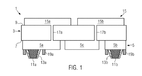
Fig. 1 schematically shows a module 1 for integrating into a card body (not
illustrated) of a
smart card (not illustrated) in accordance with some illustrative embodiments
of the present
disclosure. As illustrated in Fig. 1, the module 1 comprises a support 3, a
contact portion 5a
formed on a first surface 7 of the support 3, and a solder material lla formed
on the contact
portion 5a. A surface of the solder material lla may be at least partially
covered by a flux 13a.
In accordance with some illustrative embodiments herein, the support 3 may be
a dielectric
material layer or dielectric foil. In some illustrative examples, the support
3 may be an injection
molding body or it may represent a carrier substrate of a flexible PCB, such
as a plate made
of PCB, and the like.
With continued reference to Fig. 1, the contact portion 5a formed on the first
surface 7 of the
support 3 may represent a contact portion of a plurality of contact portions
5a, 5b, 5c
representing an inner contact structure of the module 1. Each of the contact
portions 5a to 5c
may be spaced apart from a neighboring contact portion on the first surface 7
of the support
3. Alternatively, at least some of the contact portions 5a to 5c may be
connected by a
connecting line (not illustrated). At least some of the contact portions 5a to
5c may have a
solder material formed thereon, e.g. solder material 11a on the contact
portion 5a and solder
material llb on contact portion 5b. Similar to the solder material 11a on the
contact portion
5a the solder material llb on the contact portion 5b may have a flux 13b
formed on the solder
material 11b, at least partially covering a surface of the solder material
11b.
For example, and as illustrated in the drawing of Fig. 1, the flux 13a and/or
13b may cover a
sidewall surface of the solder material 11a and 11b. However, this does not
pose any limitation
on the present disclosure and a surface of the solder material 11a, 11 b
parallel to the first
surface 7 may be also at least partially covered by the flux 13a, 13b.
In accordance with some illustrative embodiments of the present disclosure,
the flux 13a and
13b may be provided by flux residuals that may remain from flux deposited
beforehand on the
solder material 11a, lib when subjecting the solder material 11a, lib to a
reflow process
when forming a solder bump for each of the solder materials 11a, 11 b where
the flux is
deposited for providing a good wettability on the contact portions 5a and 5b
in order to
establish a good solder joint. The flux 13a, 13b may be unreacted flux
material that did not
9
CA 03218135 2023- 11- 6
WO 2022/243717
PCT/IB2021/000487
reduce an oxide during the reflow process to which the solder materials 11a,
llb are subjected
to. Due to the flux 13a, 13b, the module 1 may be equipped with flux material
without the need
of adding additional flux when implanting the module 1 into a card body (not
illustrated) of a
smart card (not illustrated) when fabricating the smart card (not
illustrated). In this way,
additional material deposition steps and inclusion of additional materials
during the fabrication
processes is avoided and the fabrication process may be simplified, as well as
productions
costs in the preparation of modules may be reduced.
In accordance with some illustrative embodiments of the present disclosure,
the solder
material 11a, 1 1 b as schematically shown in Fig. 1 may represent reflowed
solder material
with flux residuals formed at least partially on the solder bump. With the
flux 13a, 13b
representing residual flux material in some special illustrative examples, it
is possible to reduce
the total amount of flux when preparing the module 1, thereby avoiding
additional steps of
removing flux material, including remaining active flux portions. Such a
removal of flux material
would expose the module 1 to chemical flux removing agents that could lead to
undesired
corrosion in the module 1 and, accordingly, such a removal is avoided in the
present
disclosure.
Referring to Fig. 1, a barrier element 19a may be formed on the contact
portion 5a and a
barrier element 19b may be formed on the contact portion 5b. Each of the
barrier elements
19a, 19b may be formed such that the respective one of the solder materials
11a, llb is at
least partially surrounded by the barrier element 19a, 19b. In providing the
barrier element
19a, 19b in some illustrative examples, it is possible to more accurately
locate the solder
materials 11a, llb over the contact portions 5a, 5b. Furthermore, the barrier
elements 19a,
19b may help in avoiding migration of solder material into undesired regions
of the module 1
and/or a card body (not illustrated) of a smart card (not illustrated) when
fabricating a smart
card by implanting the module 1 into the card body (not illustrated) of the
smart card (not
illustrated) under fabrication. However, the person skilled in the art will
appreciate that the
barrier elements 19a, 19b are optional and may be avoided in some illustrative
embodiments
of the present disclosure. In some illustrative examples herein, the barrier
elements 19a, 19b
may be formed by depositing a pattern of solder resist on the contact portions
5a and 5b.
With ongoing reference to Fig. 1, a second surface 9 of the support 3 is
shown, the second
surface 9 representing a surface opposite the first surface 7 of the support
3. The second
surface 9 may have additional contact portions 15a, 15b provided thereon, the
contact portions
15a and 15b representing an external contact structure of the module 1 by
means of which
the module 1 being implanted into a card body (not illustrated) of a smart
card (not illustrated)
may allow access to the inner contact structure 5 of the module 1. At least
one of the contact
CA 03218135 2023- 11- 6
WO 2022/243717
PCT/IB2021/000487
portions 15a and 15b may be electrically connected with at least one of the
contact portions
5a to 5c by a via, such as a via 17a possibly connecting the contact portion
15a with the
contact portion 5a and a via 17b possibly connecting the contact portion 15b
with the contact
portion 5c. However, this does not pose any limitation on the present
disclosure and, instead
of a single via extending along a thickness direction of the support 3 through
the support 3
between the surfaces 7 and 9, one or more vertical conducting lines may be
embedded into
the support 3 for laterally routing an electrical connection between contact
portions on the first
surface 7 and contact portions on the second surface 9.
In accordance with some illustrative embodiments of the present disclosure,
the module 1 may
be one of a contact arrangement, a sensor module, and a display module. For
example, at
least one of the contact portions of the external contact structure 15 may
serve as a sensor
electrode of a sensor (not illustrated) integrated into the module 1.
Additional or alternatively,
at least one of the contact portions of the external contact structure 15 may
be operatively
connected with a displaying unit (not illustrated) of the module 1 such that
the display unit (not
illustrated) may be in electrical communication with the internal contact
structure 5 of the
module 1.
Fig. 2 schematically shows a module 1' for integrating into a card body (not
illustrated) of a
smart card (not illustrated) in accordance with some illustrative embodiments
of the present
disclosure. As illustrated in Fig. 2, the module 1' comprises a support 3', a
contact portion 5a'
formed on a first surface 7' of the support 3', and a solder material 11 a'
formed on the contact
portion 5a'. A surface of the solder material 11a' may be at least partially
covered by a flux
13a'.
In accordance with some illustrative embodiments herein, the support 3' may be
a dielectric
material layer or dielectric foil. In some illustrative examples, the support
3' may be an injection
molding body or it may represent a carrier substrate of a flexible PCB, such
as a plate made
of PCB, and the like.
With continued reference to Fig. 2, the contact portion 5a' formed on the
first surface 7' of the
support 3' may represent a contact portion of a plurality of contact portions
5a', 5b', Sc'
representing an inner contact structure of the module 1'. Each of the contact
portions 5a' to
5c' may be spaced apart from a neighboring contact portion on the first
surface 7' of the
support 3'. Alternatively, at least some of the contact portions 5a' to 5c'
may be connected by
a connecting line (not illustrated). At least some of the contact portions 5a'
to 5c' may have a
solder material formed thereon, e.g. solder material 11a' on the contact
portion 5a' and solder
material 11 b' on contact portion 5b'. Similar to the solder material 11a' on
the contact portion
11
CA 03218135 2023- 11- 6
WO 2022/243717
PCT/IB2021/000487
5a' the solder material 11b' on the contact portion 5b' may have a flux 13b'
formed on the
solder material 11 b', at least partially covering a surface of the solder
material 11 b'.
For example, and as illustrated in the drawing of Fig. 2, the flux 13a' and/or
13b' may cover a
sidewall surface of the solder material 1 1 a' and lib'. However, this does
not pose any
limitation on the present disclosure and a surface of the solder material 11
a', 11 b' parallel to
the first surface 7' may be also at least partially covered by the flux 13a',
13b'.
In accordance with some illustrative embodiments of the present disclosure,
the flux 13a' and
13b' may be provided by flux residuals that may remain from flux deposited
beforehand on the
solder material 11 a', 11 b' when subjecting the solder material 11 a', 11 b'
to a reflow process
when forming a solder bump for each of the solder materials 11 a', 11 b'. This
means, the flux
13a', 13b' may be unreacted flux material that did not reduce an oxide during
the reflow
process to which the solder materials 11a', 11 b' are subjected to. Due to the
flux 13a', 13b',
the module 1' may be equipped with flux material without the need of adding
additional flux
when implanting the module 1' into a card body (not illustrated) of a smart
card (not illustrated)
when fabricating the smart card (not illustrated). In this way, additional
material deposition
steps and inclusion of additional materials during the fabrication processes
is avoided and the
fabrication process may be simplified, as well as productions costs in the
preparation of
modules may be reduced.
In accordance with some illustrative embodiments of the present disclosure,
the solder
material 11 a', lib' as schematically shown in Fig. 2 may represent reflowed
solder material
with flux residuals formed at least partially on the solder bump. With the
flux 13a', 13b'
representing residual flux material in some special illustrative examples, it
is possible to reduce
the total amount of flux when preparing the module 1', thereby avoiding
additional steps of
removing flux material, including remaining active flux portions. Such a
removal of flux material
would expose the module 1' to chemical flux removing agents that could lead to
undesired
corrosion in the module land, accordingly, such a removal is avoided in the
present
disclosure.
Referring to Fig. 2, a barrier element 19a' may be formed on the contact
portion 5a' and a
barrier element 19b' may be formed on the contact portion 5b'. Each of the
barrier elements
19a', 19b' may be formed such that the respective one of the solder materials
11 a', 11 b' is at
least partially surrounded by the barrier element 19a', 19b'. In providing the
barrier element
19a', 19b' in some illustrative examples, it is possible to more accurately
locate the solder
materials 11 a', 11 b' over the contact portions 5a', 5b'. Furthermore, the
barrier elements 19a',
19b' may help in avoiding migration of solder material into undesired regions
of the module 1'
12
CA 03218135 2023- 11- 6
WO 2022/243717
PCT/IB2021/000487
and/or a card body (not illustrated) of a smart card (not illustrated) when
fabricating a smart
card by implanting the module 1' into the card body (not illustrated) of the
smart card (not
illustrated) under fabrication. However, the person skilled in the art will
appreciate that the
barrier elements 19a', 19b' are optional and may be avoided in some
illustrative embodiments
of the present disclosure. In some illustrative examples herein, the barrier
elements 19a', 19b'
may be formed by depositing a pattern of solder resist on the contact portions
5a' and 5b'.
With ongoing reference to Fig. 2, a second surface 9' of the support 3' is
shown, the second
surface 9' representing a surface opposite the first surface 7' of the support
3. The second
surface 9' may have additional contact portions 15a', 15b' provided thereon,
the contact
portions 15a' and 15b' representing an external contact structure of the
module 1' by means
of which the module 1' being implanted into a card body (not illustrated) of a
smart card (not
illustrated) may allow access to the inner contact structure 5' of the module
1'. At least one of
the contact portions 15a' and 15b' may be electrically connected with at least
one of the
contact portions 5a' to 5c' by a via, such as a via 17a' possibly connecting
the contact portion
15a' with the contact portion 5a' and a via 17b' possibly connecting the
contact portion 15b'
with the contact portion 5c'. However, this does not pose any limitation on
the present
disclosure and, instead of a single via extending along a thickness direction
of the support 3'
through the support 3' between the surfaces 7' and 9', one or more vertical
conducting lines
may be embedded into the support 3' for laterally routing an electrical
connection between
contact portions on the first surface 7' and contact portions on the second
surface 9'.
In accordance with some illustrative embodiments of the present disclosure,
the module 1'
may be one of a sensor module, a display module, and an arbitrary chip module.
For example,
at least one of the contact portions of the external contact structure 15' may
serve as a sensor
electrode of a sensor (not illustrated) integrated into the module 1'.
Additional or alternatively,
at least one of the contact portions of the external contact structure 15 may
be operatively
connected with a displaying unit (not illustrated) of the module 1 such that
the display unit (not
illustrated) may be in electrical communication with the internal contact
structure 5 of the
module 1.
Still referring to Fig. 2, the module 1' further has a chip package 21'
mounted to the module
1' over the first surface 7' of the support 3'. By way of example, and as
illustrated in Fig. 2, the
chip package 21 may be formed on the contact portion 5c' such that a chip 22'
is attached to
the contact portion 5c' and coupled via wire bonding 23' and 24' to respective
ones of the
contact portions 5a' and 5b'. The chip 22' may be further encapsulated by an
encapsulant 24'
covering and protecting the chip 22' and the wire bonding 23', 24'.
Accordingly, the chip
package 21' may be in electrical communication with the internal contact
structure 5'.
13
CA 03218135 2023- 11- 6
WO 2022/243717
PCT/IB2021/000487
Additionally, the chip package 21' may be in electrical communication with the
external contact
structure 15' such that the chip package 21' may be electrically accessed via
at least one of
the internal contact structure 5' and the external contact structure 15'.
With regard to Fig. 3, a smart card 30 is schematically illustrated in a cross
sectional view,
where for an ease of illustration, only an enlarged portion of the smart card
30 is schematically
illustrated. Fig. 3 shows the enlarged portion of the smart card 30 at a
module 1' corresponding
to the module 1' described above. The module 1' is accommodated into a card
body 31 of the
smart card 30. That is, the smart card 30 comprises the card body 31 of the
smart card 30
having at least one recess 37 formed therein and the module 1' being
accommodated into the
recess 37. The module 1' is in correspondence with the module 1' of Fig. 2
above and a
description of the module 1' is therefore omitted for ease of description.
This does not pose
any limitation on the present disclosure and the person skilled in the art
will appreciate that
instead of the module 1', the module 1 of Fig. 1 above may be accommodated
into the recess
37. Furthermore, the person skilled in the art will appreciate that the card
body 31 may have
at least one additional recess (not illustrated) formed therein for
accommodating at least one
additional module (not illustrated).
In accordance with the illustrative embodiment depicted in the drawing of Fig.
3, the card body
31 has an internal contact structure 33 embedded therein, the internal contact
structure 33
comprising internal connection lines 33a and 33h with each having a respective
body contact
portion 35a and 35b. The body contact portion 35a is in electrical contact
with the contact
portion 5a' of the module 1' through a solder connection 11a". Similarly, the
contact body
portion 35b is in electrical connection with the contact portion 5b' of the
module 1' via a solder
connection 11b". Accordingly, the chip package 21' may be in electrical
communication with
the internal connection structure 33 of the card body 31. Therefore, the chip
package 31' is
electrically accessible via the external contact structure 15' of the module
1' and the internal
connection structure 33 of the card body 31. In some special illustrative
examples, the internal
connection structure 33 may represent an internal connection to an antenna
(not illustrated)
which is embedded into the card body 31.
With ongoing reference to the illustration in Fig. 3, the module 1' may be
additionally attached
to the card body 11 by means of an adhesive 41a and 41b provided at the
contact portions
35a and 35b.
In accordance with the illustrative example shown in Fig. 3, some residual
flux 14a and 14b
may be present, at least partially covering a surface of the solder connection
11 a" and 11b",
respectively. The flux 14a and 14b, respectively, may allow to reduce
oxidation that possibly
14
CA 03218135 2023- 11- 6
WO 2022/243717
PCT/IB2021/000487
occurs during the fabrication of the smart card at the body contact portions
35a and 35b,
respectively. Furthermore, the flux 14a, 14b helps to gain good wettability on
the body contact
portions 35a and 35b in order to establish a good solder joint. The person
skilled in the art,
will appreciate that upon leaving residual flux 14a and 14b at the body
contact portions 35a
and 35b, corrosion of the body contact portion 35a, 35b is avoided because no
chemical flux
removing agent is employed during the fabrication of the smart card 30.
With ongoing reference to Fig.3, the recess 37 may be formed in the shape of a
stepped
recess having a deeper opening 39 at the bottom of the recess 37 to
accommodate the chip
package 21' of the module 1'. However, this does not pose any limitation on
the present
disclosure and the person skilled in the art will appreciate that the opening
39 is optional and
no opening 39 may be present in case of the module 1 of Fig. 1.
Referring to Fig. 4, a top view of a layout 50 of a smart card 51 is shown, as
obtained in
accordance with an x-ray imaging of the smart card 51. The smart card 51 is
illustrated at the
stage during fabrication at which no module is implanted into the smart card
51 yet. According
to the layout 50 as showing in Fig. 4, the smart card 51 at the depicted stage
has a body
contact portion 53 and a body contact portion 55 embedded into a card body of
the smart card
51. The body contact portions 53 and 55 are connected with an antenna module
57 and an
internal interconnection line 59. It is therefore possible to contact the
antenna module 57 via
the body contact portion 53, as well as contacting the antenna module 57 via
the body contact
portion 55 through the interconnection line 59. A portion of the smart card
layout 50 around
the body contact portion 55 as indicated by reference numeral 60 is shown in
an enlarged
view in Fig. 5.
Fig. 5 showing an enlarged view of the region 60 in Fig. 4, schematically
illustrates in greater
detail the body contact portion 55 of Fig. 4. In particular, the body contact
portion comprises
a plurality of wire pads which are schematically indicated by arrows 55 and 56
in the illustration
of Fig. 5. The wire pads are formed by a meander like arrangement of an
electric wire 58
which partially covers a plane region in the illustration of Fig. 5.
Furthermore, as indicated in
Fig. 5, an arrangement of contact pads is indicated via regions 61, showing a
location of
contact pads of a module (not illustrated) which is to be brought into contact
with the body
contact portion 55. That is, each of the plurality of contact pads 61 is
brought into electrical
contact with a respective one of a plurality of wire pads 56 of the body
contact portion 55. Due
to the meander like arrangement of wires in each of the wire pads 56 it can be
assured that a
sufficient electrical contact between the contact pad 61 and a respective wire
pad 56 is
established.
CA 03218135 2023- 11- 6
WO 2022/243717
PCT/IB2021/000487
As illustrated in the drawing of Fig. 5, each wire pad maybe formed by an
arrangement of
electrical wires that extend in a meander like fashion in the region of a
respective wire pad 56.
For example, each wire pad may consist of a plurality of wires extending
substantially in
parallel along a length direction of the arrangement and in parallel along a
width direction of
the arrangement. Herein, the length direction represents a direction along a
longest dimension
of the arrangement, while a width direction is oriented substantially
perpendicular thereto.
Furthermore, either one of the length direction and the width direction of the
arrangement is
slanted with regard to a sidewall of a cavity (not illustrated) which is to be
milled into the card
body at the location of the body contact portion 55 for accommodating a module
(not
illustrated). For example, tilting of meander like extending wires may be
under an orientation
of 00 to about 80 with regard to a cavity edge (not illustrated).
Additionally or alternatively, a
tilting of wires of a wire pad may be oriented under an angle of about 00 to
about 450 with
regard to a wire of the internal interconnection line 59 in Fig. 4.
In accordance with some illustrative embodiments of the present disclosure,
wires of a wire
pad 56 may be made of copper or a copper alloy. In some specific illustrative
examples, a wire
may be given by an isolated wire or by a non-isolated wire. A diameter of a
wire may be in a
range from 50 pm to about 300 pm, preferably in a range from 50 pm to about
200 pm or from
about 80 pm to about 300 pm, more preferably in a range from about 80 pm to
about 200 pm.
Accordingly, it is possible to combine a specific wire diameter with small
wire pitch. For
example, a wire diameter of about 112 pm may be combined with a wire pitch in
the range
from about 150 to 290 pm. Basically, with decreasing wire diameter, the wire
pitch is
decreased and, vice versa, for increasing wire diameter, the wire pitch may be
increased
accordingly. In this way it becomes possible to deviate a given wire pad
having a wire diameter
of about 112 pm and about 300 pm. As a result, a good solder connect may be
achieved by
using only some small amount of flux (e.g., a small amount of flux residuals)
so as to have a
larger metal area presented to the solder bump and it is ensured that already
a small amount
of flux, e.g., flux residuals, is sufficient for wetting wires of a wire pad
at the region near a
contact pad.
Referring to Figs. 6a and 6b, a contact portion 70 in accordance with some
illustrative
embodiments of the present disclosure will be described. Fig. 6a shows
schematically a top
view onto the contact portion 70, while Fig. 6b schematically shows a cross
sectional view of
the contact portion 70 along a line B-B in Fig. 6a. The contact portion 70 has
a solder material
71, e.g. a solder bump, formed over the contact portion 70. In accordance with
some
illustrative examples, a contact pad 73 may be provided directly on the
contact portion 70 and
the solder material 71 may be formed on the contact pad 73. The contact pad 73
may have
16
CA 03218135 2023- 11- 6
WO 2022/243717
PCT/IB2021/000487
any desired shape, e.g. an oval shape, a strip like shape, a rectangular
shape, a round shape
or any polygonal shape when seen in a top view.
With ongoing reference to Figs. 6a and 6b and in accordance with some
illustrative
embodiments of the present disclosure, a barrier element 75 may be formed on
the contact
portion 70, the barrier element 75 surrounding the solder material 71. For
example, the barrier
element 75 may be a ring shaped element or oval shape or general circular
shape when seen
in a top view, surrounding the solder material 71 and the contact pad 73. In
some illustrative
examples herein, the barrier element 75 may be formed by depositing a
patterned solder resist
on the contact portion 70.
In accordance with some special illustrative examples, a spacing B2 of the
barrier element to
the contact pad 73 may be smaller than a spacing of B3 of the barrier element
75 to the solder
material 71. The spacing B2 may be in general equal to or greater than 0 (B2
0), while the
spacing B3 maybe in general greater than 0 (B3 > 0). That is, the barrier
element 75 may be
placed directly adjacent to the contact pad 73, including the case of the
barrier element 75
being positioned on top of the contact pad 73 adjacent to the solder material
71. The barrier
element 75 may allow to locate and define a position of the solder material 75
at a certain
position over the contact portion 70. Furthermore, the barrier element 75 may
serve as a
barrier against a migration of material of the solder material 71 outside the
contact pad 73.
Referring to Fig. 6b a height H3 of the contact pad 73 is generally less than
a height H4 of the
solder material 71 (H3 < H4). Furthermore, a height H2 of the barrier element
75 is preferably
smaller than a combined height of the contact pad 73 and the solder material
71, i.e. H2 5
H3+H4. In this way, it is insured that the solder material 71 may come into
contact with a body
contact portion (not illustrated) of a card body (not illustrated).
In accordance with some illustrative embodiments and as shown in Figs. 6a and
6b, an
adhesive layer 77 may be formed over the contact portion 70 around the barrier
element 75.
The adhesive layer 77 may be spaced from the barrier element 75 by a spacing
B1. The
spacing B1 is preferably greater than 0 (B1 > 0). In some illustrative
examples herein, the
adhesive layer 77 may be provided by a hot melt, and the like. A height H1 of
the adhesive
layer 77 is in general greater than the height H2 of the barrier element 75
and smaller than
the combined height of the contact pad 73 and the solder material 71, i.e. H2
< H1 5 H4+H3.
In accordance with some alternative embodiments (not illustrated in Fig. 6),
the spacing B2
may be smaller zero (B2 < 0) which means that the barrier element 75 may be
located on the
contact pad 73 such that an upper surface of the contact pad 73 is partially
covered by the
17
CA 03218135 2023- 11- 6
WO 2022/243717
PCT/IB2021/000487
barrier element 75. In this case, the height H1 is greater than a sum of
height H2 and height
H3 (H1 > H2-FH3).
Referring to Fig. 7, a contact portion 70' is schematically shown in a top
view, the contact
portion 70' having a solder material 71' formed over the contact portion 70',
e.g. a solder bump.
The solder material 71' maybe provided on a contact pad 71' which is formed on
the contact
portion 70'. The contact pad 73' may be similar to the contact pad 73 as
described above with
regard to Fig. 6a and 6b.
In accordance with some illustrative embodiments and as shown in Fig. 7, the
contact pad 73'
may be partially surrounded by a barrier element 75', leaving access to the
contact pad 73'
from outside a region surrounded by the barrier element 75'. Accordingly, a
conductor line 74
extending on the contact portion 70' to the contact pad 73' may pass through
an opening in
the barrier element 75' for contacting the contact pad 73'. Accordingly, the
contact pads 73'
may be electrically connected with an internal connection of the module (not
illustrated)
outside the contact portion 70'. In some illustrative examples herein, the
barrier element 75'
may be formed by depositing a patterned solder resist on the contact portion
70'.
In accordance with some illustrative examples in alternative embodiments (not
illustrated in
Fig. 7), the conductor line 74 may have a mirco etching instead of using the
barrier layer
portion 75' near the opening in order to created a recess in the conductor
line 74, thereby
providing another kind of barrier layer as a stop line to prevent solder from
running along the
conductor line 74.
The barrier element 75' may be in dimension similarly to the barrier element
75 as described
above with regard to Fig. 6b. In particular, dimensions of the solder material
71', the contact
pad 73', the barrier limit 75' and an adhesive layer (not illustrated in Fig.
7) may correspond
to dimensions as discussed above to the corresponding elements shown in Fig.
6b.
The opening 76 in the barrier element 75' may correspond to a recess in the
barrier element
75' removing at most 40% of the barrier element 75 in Fig. 6b when set into
relation.
Referring to Fig. 8a, a contact portion 80, in accordance with some
illustrative embodiments
of the present disclosure, is schematically shown. For ease of illustration,
the contact portion
80 is only shown with regard to a contact pad 82 having a barrier element 83
to illustrate a
spatial relation and arrangement of the barrier element 83 with regard to the
contact pad 82.
A solder material 85 is present, e.g. in form of a solder bump, corresponding
to the solder
material 71 and 71' as described above with regard to Figs. 6a, 6b and 7.
However, the
illustrative embodiments of Fig. 8a differ from the illustrative embodiments
as described above
18
CA 03218135 2023- 11- 6
WO 2022/243717
PCT/IB2021/000487
in that the barrier element 83 has a negative spacing with regard to the
contact pad 82 or, in
other words, the barrier element 83 is formed on the contact pad 82.
Additionally, it is possible
that the barrier element 83 is provided as a partially surrounding barrier
element corresponding
to the barrier element 75' of Fig. 7. It may be considered that the
illustrative embodiments as
shown with regard to Fig. 8a represent a case in which a spacing between the
barrier element
83 and the contact pad 82 is negative.
With regard to Fig. 8b, some illustrative embodiments of the embodiments of
Fig. 8a will be
described. Fig. 8b schematically shows a cross-sectional view of Fig. 8a along
line B-B in Fig.
8a. In these illustrative embodiments, the barrier element 83 of Fig. 8a may
be formed by
providing the contact pad 82 having a recess 87 in a center portion of the
contact pad 82, the
recess being formed by microetching, for example. Accordingly, the contact pad
82 comprises
the recess 87 as the center portion of the contact pad 82 having an upper
surface located
higher than an upper surface of a rim or wall portion of the contact pad 82
encircling the recess
87 and forming the barrier element 83. In other words, the barrier element 83
provides a wall
that is acting as the barrier element 83 with regard to the solder material
85, e.g., representing
a solder bump, placed in the recess 87.
Referring to Fig. 9a, another illustrative embodiment of the present
disclosure is schematically
illustrated in a top view, while Fig. 9b shows a schematic cross sectional
view along line B-B
in Fig. 9b.
Referring to Fig. 9a and 9b, a contact portion 90 of a support, e.g., a PCB
substrate or a tape
or any other appropriate carrier element, is shown. The contact portion 90 has
a contact pad
93 and a barrier element 95 which at least partially surrounds the contact pad
93. In some
illustrative example herein, the barrier element 95 may be formed by
depositing a solder resist
on an upper surface of the contact portion 90. Alternatively or additionally,
the barrier element
may be provided by patterning the upper surface of the contact portion 90 so
as to realize the
barrier element 95 in the upper surface of the contact portion 90.Referring to
Fig. 9b, a
thickness of the contact pad 93 may be smaller than a height of barrier
element 95.
In accordance with some illustrative examples herein, a barrier pattern 96a
comprising at least
one barrier line may be formed on the contact pad 93. For example, and as
illustrated without
limitation in Fig. 9a, the barrier pattern 96a may be formed by a barrier
array comprising barrier
lines 96b, 96c which may be arranged in an orthogonal array comprising at
least one barrier
line extending along a first direction, e.g., the barrier line 96b, and at
least one barrier line
extending along a second direction which is substantially perpendicular to the
first direction,
e.g., the barrier line(s) 96c. For example and as illustrated in Fig. 9a, the
barrier pattern 96a
19
CA 03218135 2023- 11- 6
WO 2022/243717
PCT/IB2021/000487
comprises a plurality of barrier lines being formed by the barrier line 96c
and at least one
additional parallel barrier line 96c is arranged so as to be orthogonal to the
barrier line 96b.
As shown in Fig. 9b and in accordance with some illustrative examples, the
barrier pattern
96a may be formed by one or more micro-etchings that are provided in an upper
surface of
the contact pad 93. For example, the barrier pattern 96a may comprise one or
more trenches
formed by micro-etching subjected to the contact pad 93 or, alternatively, the
barrier array 96a
may be formed by a laser process. However, this does not pose any limitation
to the present
disclosure and, alternatively, the upper surface of the contact pad 93 may be
exposed to some
micro-etching such that one or more elevation (not illustrated), e.g., one or
more rip-shaped
elevation (not illustrated) may be formed in the upper surface of the contact
pad 93.
Additionally or alternatively, the barrier pattern 96a may comprise one or
more trenches and
one or more elevations. Accordingly, at least one barrier line of the barrier
pattern 96a may be
either a trench or an elevation formed in the upper surface of the contact pad
93 and,
optionally, at least one other barrier line of the barrier pattern 96a may be
the other one of the
trench and the elevation.
In effect, the barrier lines 96c and 96b partition the upper surface of the
contact pad 93 into a
plurality of separated sections or, in other words, the upper surface of the
contact pad 93 is
patterned by the barrier pattern 96a, such that a flow of solder material (not
illustrated) is
hindered in spreading over the upper surface of the contact pad 93 once the
solder material
(not illustrated) is molten in a reflow process, e.g., the reflow process
employed during module
integration. So to speak, the barrier pattern 96a allows to prevent or at
least slow down any
movement of solder material (not illustrated) placed on the upper surface of
the contact pad
93.
Although Fig. 9a and 9b show the barrier pattern 96a as an orthogonal array of
lines 96b, 96c,
the person skilled in the art will appreciate that this is only illustrative
and not limiting. Instead
of the explicitly shown orthogonal array of lines 96b, 96c, the barrier
pattern 96a may be
implemented in any other pattern, e.g., by curved patterns, such as oval
patterns, ring
patterns, ring portion patterns, polygonal patterns, such as squared patterns,
rectangular
patterns, a combination of curved patterns and polygonal patterns, etc.
Herein, line
sections/portions and/or curved sections/portions surrounding a center of the
contact pad,
produce a general barrier pattern.
Although none of the embodiments illustrated in Figs. 6a, 6b, 7, 8a, 8b and 9a
and 9b explicitly
show a flux, the person skilled in the art will appreciate that a flux is
formed on a surface of
CA 03218135 2023- 11- 6
WO 2022/243717
PCT/IB2021/000487
the solder materials so as to at least partially cover the solder materials
with flux material, e.g.,
sidewall surfaces of solder materials.
Although Figs. 7 to 9 do not explicitly show an adhesive layer, the person
skilled in the art will
appreciate that an adhesive layer corresponding to the adhesive layer 77 in
Fig. 6a and 6b
may be present.
Although Fig. 9a and 9b show a positive spacing between the barrier element 95
and the
contact pad 93, this does not pose any limitation on the present disclosure
and the barrier
element 95 may have a negative spacing with regard to the contact pad 93 in
analogy to the
disclosure regarding Fig. 8a and 8b above. Herein, the barrier element 95 in
Fig. 9a and 9b
would be replaced by a barrier element formed in accordance with the barrier
element 83 in
Fig. 8a and 8b.
In summary and as it will be clear to the skilled person after a complete
lecture of the
embodiments described above, the present disclosure relates, in various
illustrative
embodiments, to a module and, in at least some illustrative embodiments, to a
wire pad design
for establishing a solder connect from at least one smart card module to at
least one wire pad
provided in a recess or cavity of a card body. Herein, a solder bump may be
provided with the
module without applying external flux material during a solder process and/or
a reflow process
of the solder bump. In some illustrative embodiments of the present
disclosure, the solder
material and flux material is applied to a module first before implanting the
module into a card
body.
As an advantage, some illustrative embodiments of the present disclosure allow
an
improvement of known interconnection concepts by applying a solder and a
optionally together
with a flux material prior to implanting a module into a card body to the
module without
additionally applying a solder material to contacts in the card body before
inserting the module
into the card body.
In some illustrative embodiments of the present disclosure, a module with a
reflow solder
bump on connection pads of the module is provided, the solder bump having flux
residuals on
its surface containing active flux elements which are to be activated during
subsequent module
implanting processes in the fabrication flow of a smart card. In these
illustrative embodiments,
a contact pad may be provided as a pure contact pad or a surrounding barrier
element, which
at least partially surrounds the contact pad as a solder stop and barrier
layer may be provided.
Additionally or alternatively, an adhesive layer may be provided around the
contact pad, such
as a hot melt or the like.
21
CA 03218135 2023- 11- 6
WO 2022/243717
PCT/IB2021/000487
In accordance with some illustrative embodiments as described above, an
illustrative module
implanting process for making interconnection of a solder material contained
on a module with
a wire pad, possibly milled when forming a recess in a card body by milling
the recess into the
card body, using flux residuals is shown, the flux residuals resulting from a
possible first reflow
process subjected to solder materials so as to form solder bumps on the
module. The solder
connection is established by using the flux residuals and reactivating the
remaining active
elements of residuals on the solder material of the module. Such a solder step
comprises a
step of applying heat and pressure to the module inserted into the card body,
followed by
cooling step.
In accordance with some illustrative embodiments of the present disclosure, a
support of an
illustrative module as described above by means of the support 3 and 3' may be
made of e.g.
tape (such as epoxy-glass tape), PI, PEN, PET and the like.
In accordance with some illustrative embodiments as described above, a barrier
element may
be provided for at least partially controlling a spreading of solder material
during the
implantation of a module into a card body of a smart card. Herein, the
spreading may be
particularly controlled by appropriately setting a height and shape of the
barrier element as
described above with regard to Figs. 6a, 6b, 7, 8a, 8b, 9a and 9b.
As an advantage of not using solder material in addition to the solder
material of the module,
less energy is needed for melting the solder and shorter implanting time may
be achieved.
Furthermore, due to a reduced amount of solder material employed during the
implanting of
modules into a card body as described above in the various illustrative
embodiments, the
solder is better controllable during the implantation. Furthermore, it is
found by the inventors
that less active flux remains in interconnections of accordingly implanted
modules as
described above.
An advantage of barrier elements is that a preforming of a solder bump shape
may be
achieved, e.g. a longitudinal solder bump may be formed using an oval contact
pad, optionally
together with an appropriate barrier element, for providing a solder bump that
perfectly
corresponds to a high density wire pad of a card body. A controlling of the
position of solder
on the module can be further supported by an adhesive layer surrounding the
contact pad on
which a solder material is provided in the module.
At least one of the following advantages may be achieved when practicing the
subject matter
of the present disclosure in accordance with at least one of the various
described
embodiments:
22
CA 03218135 2023- 11- 6
WO 2022/243717
PCT/IB2021/000487
A strong solder connect between a module and a card body of a smart card may
be achieved.
No additional solder material or flux is to be provided during the
implantation of a module into
a card body of a smart card.
Solder and flux, that is remaining active flux in flux residuals from a first
reflow of solder, may
be pre-applied on the module, particularly on a solder bump of a module.
A comparatively large solder connect is possible due to a freedom in the
choice of shape of
solder bump, such as an oval shape of solder bump, thereby increasing the
reliability of a
solder interconnect.
The various illustrative embodiments described above provide a relatively easy
processing
during the implanting compared to known solder connect techniques.
The various illustrative embodiments as described above allow to use a wire
pad which
provides a large wire pad area accessible for performing solder connects.
According to the various illustrative embodiments as described above, less
remaining active
flux residuals may remain present in the final interconnect, thereby leading
to less corrosion
in fabricated smart card.
Employing barrier elements in module according to at least some of the above
described
illustrative embodiments, allow to prevent wide solder spreading during
implantation when
forming a smart card.
With regard to any of the above described embodiments, it is to be understood
that a solder
material may be deposited on a contact pad by depositing a plurality of solder
portions on the
contact pad, e.g., several hundreds of ball-shaped solder portions, which are
in reflown in a
reflow process to form a single solder bump. This solder bump may be exposed
to a second
reflow process during module integration, wherein solder bump(s) of a module
are brought
into mechanical contact with substrate contact(s) of a substrate into which
the module it to be
integrated or to which the module is to be connected. Upon applying heat and
pressure during
a certain time period, e.g., up to 3 s, the solder bump(s) is/are reflown so
as to provide
mechanical and electrical connection of the module to the substrate
contact(s).
These and other advantages will become apparent to the person skilled in the
art who has the
benefits of the present disclosure.
23
CA 03218135 2023- 11- 6