Note: Descriptions are shown in the official language in which they were submitted.
WO 2022/232952
PCT/CA2022/050727
SYSTEM AND METHOD FOR HAPTICS USING SHAPE MEMORY MATERIAL
Cross-reference to Other Applications
[0001] The application claims the benefit of priority from US
Provisional Application
No. 63/185,485 filed May 7, 2021 which is hereby incorporated by reference.
Field
[0002] The present disclosure relates generally to haptic
devices. More particularly,
the present disclosure relates to a system and method for haptics using shape
memory
material.
Background
[0003] Haptic devices are used in many varieties of products and
in many markets.
These products use various types of actuators to stimulate the sense of touch.
One of the
main factors inhibiting the deployment of haptic technology is the cost.
Additionally, the size
and weight of many systems prohibits, or reduces, their range of use, limiting
viable use
scenarios such as take-home training for medical students and portable
gaming/entertainment. Some important performance metrics common to haptic
devices
include the following: degrees of freedom (DOF); work volume; position
resolution;
continuous force ability; maximum force/torque; maximum stiffness; frequency;
inertia and
the like. Finding a balance among these parameters presents a challenge as
current
actuation mechanisms compromise on various metrics to improve upon others.
[0004] Electromagnet actuators can be used for haptic devices
due to high
achievable forces, low impedance and relatively simple, robust control
algorithms. One of the
large limitations of electromagnetic actuators is their low force density,
significantly
increasing their size and weight in order to increase achievable forces. Due
to their increased
weight, another limitation is their high endpoint inertia. This may be
minimized by employing
parallel rather than serial manipulator designs, or by integrating gearing. As
a trade-off,
gearing will add its own friction, inertia and backlash, compromising the
impedance of the
system. Furthermore, a continuous force is generally unachievable.
[0005] Compared to electromagnetic actuators, piezoelectrics
have a higher force
density, providing greater force with lower volumes. However, a limitation is
the amount of
- 1 -
CA 03218137 2023- 11- 6
WO 2022/232952
PCT/CA2022/050727
actuation that can be achieved due to the fact that their mechanism relates to
a principle of
deformation. The application of piezoelectrics in haptics is typically limited
to very small
working spaces. Additionally, piezoelectrics have higher power supply
requirements
compared to electromagnetic actuators. Further limitations for piezoelectrics
in the
application of haptics include operating temperature, voltage and mechanical
stress. Though
these properties may be tweaked to an extent, costs and response times will
typically be
compromised.
[0006] Fluid that can change in viscosity when applying a
magnetic field or electric
current may sometimes be used as actuators for haptic devices. There are two
main types of
smart fluids ¨ magnetorheological (MR) and electrorheological (ER), controlled
by magnetic
and electric fields, respectively. The main advantage of MR fluids is the
large force that they
can resist, however a large magnet is required which adds to a bulk of the
system. The main
advantage of ER fluids is the small size of the actuating elements relative to
MR fluids. Smart
fluids have a high force density, low inertia and negligible backlash. One
limitation of smart
fluid actuators is that the relationship between input current and output
torque is non-linearly
related with hysteresis, unlike electromagnetic actuators. This may be
compensated for by
implementing force/torque sensors, however this can drive up costs and add
undesired
friction, backlash and cogging to the actuators.
[0007] Therefore, there is provided a novel system and method of
using haptics using
shape memory material.
[0008] The above information is presented as background
information only to assist
with an understanding of the present disclosure. No determination has been
made, and no
assertion is made, as to whether any of the above might be applicable as prior
art with
regard to the present disclosure.
Summary
[0009] In a first aspect, the present disclosure provides a
system and method for
haptic devices that use shape memory materials.
[0010] One advantage of the current disclosure is an SMA
controlled haptic device
that improves upon at least one of the size, workspace, cost and force
restrictions of current
solutions. In particular, the system and method may use SMA actuators to
control the force
experienced at a stylus end effector, overcoming limitations of current
technology such as
- 2 -
CA 03218137 2023- 11- 6
WO 2022/232952
PCT/CA2022/050727
backlash from a gearbox, inability to provide continuous force and high
inertial losses. The
system and method may be adapted for various applications, such as gaming,
surgical
training, teleoperation, remote equipment maintenance, or many other virtual
reality
applications. In some cases, the system and method can be adapted for use in a
haptic
glove, to provide even greater portability and immersion.
[0011] In one aspect, there is provided A haptics device
including a set of haptic
arms, each haptic arm including an actuating mechanism; a set of shape memory
alloy
(SMA) components, each of the set of SMA components connected to one of the
set of
haptic arms to drive the actuating mechanism; and a processor for
communicating with each
of the actuating mechanisms to actuate the set of haptic arms.
[0012] In another aspect, the set of SMA components include a
SMA wire, a SMA
bundle, a SMA spring or a thin SMA sheet. In another aspect, when a current is
passed
through a SMA component, at least one portion of the SMA component experiences
a
microstructural transformation and at least one other portion of the SMA
component remains
unchanged. In a further aspect, the haptics device further includes a set of
cooling housings
for cooling the set of SMA components. In yet another aspect, the haptics
device further
includes a set of positioning sensors for sensing a position of the set of
haptic arms. In
another aspect, the SMA components are a SMA wire or SMA bundle. In an aspect,
the
SMA wire bundle includes crimps or swages at at least one end of the SMA wire
bundle. In
another aspect, the SMA wire bundle includes a first portion and a second
portion. In yet a
further aspect, the haptics device further includes an electrical isolating
component to isolate
the first portion of the SMA wire bundle from the second portion of the SMA
wire or SMA
bundle.
[0013] In another aspect, the haptics device further includes an
end effector, the end
effector connected to at least one of the set of haptic arms. In yet another
aspect, the
haptics device further includes a stylus component connected to the end
effector. In yet a
further aspect, each of the set of haptic arms includes a proximal linkage;
and a distal
linkage. In another aspect, the set of SMA components are processed via
multiple memory
material technology to impart the multiple local transformation temperatures
or enhance
mechanical performance. In a further aspect, at least one of the set of SMA
components
includes multiple local transformation temperatures. In another aspect, one
portion of a SMA
- 3 -
CA 03218137 2023- 11- 6
WO 2022/232952
PCT/CA2022/050727
component actuates upon heating and another portion of the SMA component
provides
sensing.
Description of the Drawings
[0014] Other aspects and features of the present disclosure will
become apparent to
those ordinarily skilled in the art upon review of the following description
of specific
embodiments in conjunction with the accompanying figures.
[0015] Embodiments of the present disclosure will now be
described, by way of
example only, with reference to the embedded Figures.
[0016] Figures la and lb are schematic diagrams of shape memory
material
undergoing a multiple memory material process;
[0017] Figures 2a to 2c are schematic diagrams of a haptic
device using shape
memory materials;
[0018] Figure 3 is a perspective view of the haptic device of
Figures 2a to 2c;
[0019] Figure 4 is a front view of a haptic device with arms in
a delta formation;
[0020] Figure 5 is a perspective view of a haptic arm;
[0021] Figures 6a and 6b are side and perspective views of how
SMA material is
connected to the haptic arm;
[0022] Figure 6c is a flowchart outlining a method of actuating
a haptics device;
[0023] Figure 7 is a perspective view of a cooling housing;
[0024] Figure 8a is a schematic view of airflow within a cooling
housing;
[0025] Figure 8b is a schematic cross-section of a view of a
cooling housing
integrated with a haptic arm;
[0026] Figure 8c is a schematic view of a set of cooling
housings integrated on
actuator brackets;
[0027] Figure 9 are a set of drawings of end effector mounts and
stylus;
[0028] Figures 10a to 10c are perspective views of a housing for
the haptic device;
and
[0029] Figures lla to 11h are different views of haptic glove.
- 4 -
CA 03218137 2023- 11- 6
WO 2022/232952
PCT/CA2022/050727
Detailed Description
[0030] The following description with reference to the
accompanying drawings is
provided to assist in understanding of example embodiments as defined by the
claims and
their equivalents. The following description includes various specific details
to assist in that
understanding but these are to be regarded as merely examples. Accordingly,
those of
ordinary skill in the art will recognize that various changes and
modifications of the
embodiments described herein can be made without departing from the scope and
spirit of
the disclosure. In addition, descriptions of well-known functions and
constructions may be
omitted for clarity and conciseness.
[0031] The terms and words used in the following description and
claims are not
limited to the bibliographical meanings, but, are merely used to enable a
clear and consistent
understanding. Accordingly, it should be apparent to those skilled in the art
that the following
description of embodiments is provided for illustration purpose only and not
for the purpose
of limiting the invention as defined by the appended claims and their
equivalents.
[0032] In the current disclosure, shape memory material is used
to provide haptics to
components. In some embodiments, the current disclosure uses shape memory
material
that may be processed by multiple memory material (MMM) technology such as
described in
U.S. Patent No. 9,186,853, granted November 17, 2015 which is hereby
incorporated by
reference. Examples of MMM processing or technology are schematically shown in
Figures
la and lb. By applying MMM processing or technology to the smart memory
material or
smart memory alloy (SMA), precise tuning of local transformation temperatures
within the
SMA is enabled. This allows multiple transformation temperatures to be
utilized for SMAs
resulting in at least one of, a dynamic response from the SMA at distinct, or
predetermined,
temperatures, higher cycle life and/or the ability to enable sensing (such as
force and
displacement) within the SMA material. Specifically, MMM technology may be
seen as a
method for applying energy to a local area of a shape memory material to
adjust the local
structure and chemistry. The application of the MMM technology provides one or
more
additional transformation temperatures or modified pseudo-elastic properties
of the treated
local area. The remaining unaffected material still exhibits its original
functional properties,
which may include a linear elastic/plastic response such as in a fully cold
worked condition.
Hence, additional memories and properties can be realized in a monolithic SMA
component,
- 5 -
CA 03218137 2023- 11- 6
WO 2022/232952
PCT/CA2022/050727
which in turn enables additional functionality. This makes it possible to
fabricate a monolithic
SMA that can operate passively in a wide range of temperatures.
[0033]
SMAs have unique properties with two being the shape memory effect (SME)
and pseudoelasticity (PE) of the SMA. The SME results from the ability of an
alloy to
transform from a rigid, high temperature austenite phase to a malleable, low
temperature
martensite phase during cooling. Once a high temperature shape is trained into
an SMA
component in the austenite phase, it can further be cooled to its martensite
phase and
deformed. When the material is cooled below a martensitic finish temperature
(Mf), it is
entirely martensite and easily deformed. Upon heating the SMA above an
austenitic finish
temperature (Al), the material becomes entirely austenite and returns to its
trained shape,
exhibiting large forces.
Depending on the SMA's composition and historical
thermomechanical processing, the functional high temperature phase may be the
R-phase or
any other phase.
[0034]
Embodiments of the system and method herein are intended to provide
improvements in position sensing, for example, sensing change in radius of
linkages to
determine translation of end effector, applying MMM to shape memory material
to sense the
resistance based on position; provide improvements in SMA wire bundles
comprised of very
thin wires to achieve high frequency actuation; provide air channels to
precisely control
cooling of SMA bundles; and the like, as described herein. Table 1 below
provides a table
showing how use of SMA being treated by MMM technology in haptics technology
improves
over current solutions:
Current Solution Limitation SMA Comparison
Weight SMAs can have an extremely large force to weight ratio,
reducing overall weight of the actuator
Force output Higher force to weight ratio allows SMAs to exert higher
continuous force
Cost Fewer necessary components and smaller volume of
material reduces cost of system
Frictional losses Fewer mechanical components
compared to
electromagnetic drives, reducing resultant friction and
wear
- 6 -
CA 03218137 2023- 11- 6
WO 2022/232952
PCT/CA2022/050727
[0035] In some embodiments, utilizing SMAs as the actuation
driver can provide the
potential to overcome some of the limitations of current technology, such as,
but not limited
to, electromagnetic drives. A constant force can generally be applied for an
extended period
of time, the size and weight of the system can be reduced significantly, and
in turn, inertial
forces and losses can be minimized or reduced. As an example, results of
testing of a
particular embodiment yielded a force range of 0-53N, a system friction of
less than 0.1N, an
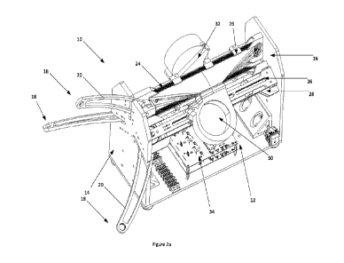
actuation frequency of 3Hz and a position resolution of <0.025%.
[0036] Figures 2a to 2c show one embodiment of an assembled
haptic device where
Figure 2a is a front perspective of the haptic device with proximal linkages
of the haptic arms
visible, Figure 2b is a rear perspective of the haptic device with proximal
linkage of the haptic
arms visible and Figure 2c is a rear perspective view of the haptic device
with proximal
linkage of haptic arms visible and electronics removed. Figure 3 is a
schematic diagram of a
haptic device with a rear portion removed so that the actuator assembly can be
more clearly
shown.
[0037] In the embodiment illustrated in Figures 2a to 2c and
Figure 3, a housing of
the device 10 includes a base 12, front plate 14 and back plate 16, which are
secured
together and act as the frame on which the rest of the components of the
haptic device can
be mounted or installed. As shown in Figures 2a to 2c, the components can be
housed within
the shell with a portion (the proximal linkages) of the haptic arms 18
protruding out of the
front plate 14.
[0038] In Figures 2a to 2c and Figure 3, only the proximal
linkages 20 of the haptic
arms 18 are shown outside the housing or shell. Figure 5 provides a
perspective view of a
full haptic arm 18 including the proximal linkages 20 and distal linkages 22
that make up
each of the three haptic arms 18.
[0039] In the current embodiment, the three haptic arms 18 are oriented in a
delta formation
or configuration (which is more clearly shown in Figure 4). A delta formation
allows the
actuators to be housed on the base 12 of the device 10 thereby reducing the
weight of the
haptic arms 18. Additionally, the cost and manufacturing complexity is
relatively low as each
of the three haptic arms 18 can be made identical. The delta formation also
offers precision
in terms of position compared to serial manipulator designs, as errors are
shared by each of
the linkages rather than added. In the current embodiment, the device 10
further includes
SMA components, such as in the form for wire bundles 24 (made up of this SMA
wires) that
- 7 -
CA 03218137 2023- 11- 6
WO 2022/232952
PCT/CA2022/050727
are wrapped around a base of the proximal linkage 20 and individually secured
to individual
actuator brackets 26 or actuation mechanisms. SMA components may also include,
but are
not limited to, a SMA spring, a SMA tube or a thin SMA sheet.
[0040] In operation, the SMA wire bundles 24 may function or
operate as a driver for
the actuating mechanism. In order to cool the SMA wire bundles 24, each
actuator bracket
26 can have a cooling housing 28 attached to it. Details with respect to the
cooling housing
28 are discussed below. Although not shown, the device also includes
electrical components
for supplying current to the SMA wire bundles.
[0041] Each cooling housing 28 links the SMA wire bundles 24 to
a fan 30. In an
alternative, other sources, or methods, of cooling such as, but not limited
to, glycol channels
or the like may be employed. Alternatively, a high temperature SMA may be
employed to
eliminate, or reduce, the need for active cooling such that ambient
temperatures may be
sufficient to cool the SMA wire bundles 24 and achieve high frequency
actuation. In the
current embodiment, the fans 30 are mounted in place by fan mounts 32 that
attach to the
adjacent actuator bracket 26.
[0042] The SMA wire bundles 24 are electrically connected to a
control board 34, or
processor, which regulates the current supply to each of the three SMA wire
bundles 24
based on the detected position of the haptic arms 18. In use, if an object is
encountered by
the haptic device in virtual space, the combination of the three actuators
allows for the force
to be experienced in three degrees of freedom (DOF).
[0043] Figure 4 is a schematic diagram of a set of haptic arms
in a delta formation
with end effector and workspace shown. Due to the nature of the delta
formation, the
workspace 40 is generally dome-shaped with a larger area at the base of the
workspace.
One benefit of this is that it is larger in the base of the work volume. The
base of the stylus
(the spherical portion) is able to translate and rotate freely within the
bounds of the
workspace.
[0044] The size of the workspace can be dictated by the length
of the proximal
linkages 20 and distal linkages 22 and the usable strain of the SMA wire
bundles 24. There is
a balance between optimizing, or improving, the workspace and minimizing, or
reducing, the
weight of the system, as more material is required not only to lengthen the
haptic arms 18
but also to strengthen them. Increasing the length of the proximal 20 or
distal 22 linkages will
directly increase the workspace at the cost of reducing the resultant forces.
- 8 -
CA 03218137 2023- 11- 6
WO 2022/232952
PCT/CA2022/050727
[0045] In operation, when the stylus is manipulated by a user,
the movement of the
stylus is sensed by the haptic arms which translates this sensed motion and
transmits
signals representative of the sensed motion to a processor such that the
processor can then
translate this sensed motion on a display to the user.
[0046] In one embodiment, high-quality, low-friction bearings
can be used in each of
the joints of the haptic system. To reduce inertial forces, the weight of the
haptic arms 18 and
end effector are minimized, or reduced, to every extent possible. In some
embodiments,
since the actuators remain in the base of the unit such as in the delta
formation design, the
weight of the actuators is less of a concern or not as big a factor in haptic
device design
compared with current solutions. The reduced weight of the SMA actuators in
the disclosure
compared to other technologies, such as electromagnetic actuators, helps to
improve the
overall portability of the system.
[0047] Figure 5 is a schematic diagram of a haptic arm with SMA
wire routing within
each haptic arm 18. The SMA wire bundles 24 actuate the haptic arms to control
a
positioning of the haptic arm 18. Further details are shown with respect to
Figures 6a and 6b
which are schematic diagrams showing inductive sensing to determine an angle
of a distal
linkage. Figure 6a is a close up schematic diagram showing a radial profile of
distal linkage
and Figure 6b is a schematic diagram showing a full SMA wire assembly and
inductive coil.
[0048] In one embodiment, the SMA wire bundles 24 controlling
the position of the
haptic arms 18 are made up of multiple SMA wires with crimps 50 on either end
to create a
single actuating unit. In other embodiments, the SMA wire or SMA bundle may
include
swages at either end. In one embodiment, the wires may be very thin
(approximately 150um
diameter or less) to allow for rapid actuation and cooling. In some
embodiments, each SMA
wire bundle 24 may include up to 20 or more individual wires. In an
alternative embodiment,
a single SMA wire may be used, or alternative forms of SMA material such as a
thin sheet, a
tube or a spring. In a thin sheet form, the material may be further cut into
thin slits using non-
thermal cutting processes (e.g. femtosecond laser or electrical discharge
machining (EDM))
to preserve the functional properties of the SMA.
[0049] The crimps 50 shown in Figures 6a and 6b can be mounted
together. In some
embodiments, the crimps 50 may be covered with an electrically resistive
material such that
they are electrically isolated. In other embodiments, the crimps 50 may be
made of stainless
steel or aluminum. Use of the crimps 50 improves an ability for the SMA
bundles to be
- 9 -
CA 03218137 2023- 11- 6
WO 2022/232952
PCT/CA2022/050727
connected with other components of the haptic device and provides connection
advantages
over other systems.
[0050] In the current embodiment, the SMA wire bundles 24 wrap
around two SMA
pulleys 52 to allow for a larger usable strain (longer wire) while minimizing,
or reducing, the
length of each SMA wire required for the overall system. To help keep the SMA
wire bundles
24 in place and avoid tangling, each of the wires may be fit through a small
channel on the
SMA pulley 52 prior to crimping the SMA wire bundle 24 ends.
[0051] As shown in Figure 6a, the SMA wire bundles 24 wrap
around a radial
protrusion 54 on the proximal linkage 20 and interfaces with a ground
connector 56 that
rigidly connects to the proximal linkage 20. The SMA wire bundle 24 may be
seen as
including at least two portions which may or may not be the same size i.e. two
halves. The
ground connector 56 electrically isolates a portion, such as each half, of the
SMA wire bundle
24 such that it can be antagonistically actuated. When current is supplied via
one of the
crimps 50, the current passes through the wire bundle until it reaches the
ground connector
56, actuating a first portion, such as half of the SMA wire bundle 24 (causing
an austenitic
transformation), while the other, or second, portion, which may be the other
half, of the SMA
wire bundle 24 remains in the cooled martensitic state. The antagonistic
biasing is intended
to remove the need for an external bias (such as a spring or deadweight) for
the SMA
actuators.
[0052] The radial protrusion 54 has a variable radius profile,
such that the radius
starts at one dimension at R1 and increases to a larger radius at R2 (Figure
6A). A small
inductive coil can be rigidly mounted beside the radial protrusion 54. As the
angle of the
proximal linkage 20 changes, the distance between the inductive coil and the
radial
protrusion 54 changes, resulting in different inductance values. The inductive
values can be
mapped to the translational position of the haptic arms 18 to provide a
reliable position
sensor for three DOF. In an alternative embodiment, MMM laser processing, such
as
disclosed in US Patent Publication No. 20180347020 entitled METHODS AND
SYSTEMS
FOR PROCESSING MATERIALS, INCLUDING SHAPE MEMORY MATERIALS; US Patent
Publication No. 20170165532 entitled MULTIPLE MEMORY MATERIALS AND SYSTEMS,
METHODS AND APPLICATIONS THEREFOR; and US Patent Publication No. 20190264664
entitled SHAPE MEMORY ALLOY ACTUATOR WITH STRAIN GAUGE SENSOR AND
POSITION ESTIMATION AND METHOD FOR MANUFACTURING SAME (which are all
- 10 -
CA 03218137 2023- 11- 6
WO 2022/232952
PCT/CA2022/050727
hereby incorporated by reference) may be used as an embedded strain gauge to
achieve
position sensing.
[0053] Turning to Figure 6c, a method of actuating a haptics
device that uses SMA
components that may or may have been MMM treated to include multiple
transformation
temperatures or to enhance mechanical performance is shown. Initially, the SMA
is treated
or processed via MMM technology so that the SMA includes multiple
transformation
temperatures (650). It is understood that this may not necessarily be part of
the method of
the disclosure as the haptics device may use SMA components that have been
previously
MMM treated or processed or may use SMA components that are not MMM treated or
processed.
[0054] The MMM treatment of the SMA causes the SMA component to
have different
portions that may react differently to different applied temperatures or
currents. In other
words, the SMA component may be seen as being made up of multiple portions or
sections.
At least one section of the SMA component is then electrically isolated from
other sections of
the SMA component (652). When a movement is sensed, current is passed through
the
SMA components (such as SMA wire bundles) (654). As the current passes through
the
SMA components, it will pass through a portion of the SMA component until it
reaches the
electrically isolating component, such as a ground connector 16, actuating
that portion of the
SMA component (causing an austenitic transformation), while the other portion
or portions of
the SMA component remains in a cooled martensitic state. It is understood that
based on a
design of the SMA components, there may be one or more portions that actuate
in response
to the applied current and one or more portions that do not react or actuate
in response to
the applied current. In some embodiments, the SMA component may include a
sensing
portion or may itself perform a sensing functionality. In some cases, the hot
and cold phase
may be different from austenite and martensite and include phases such as R-
phase
depending on the composition and thermomechanical history of the alloy.
[0055] In another embodiment, when current is passed through a SMA component
(causing
heating), at least one portion of the SMA component experiences a
microstructural
transformation and at least one other portion of the SMA component remains
unchanged.
[0056] Figure 7 is a schematic view of a cooling housing and
Figures 8a to 8b are
different cross-sections of the cooling housing. Figure 8a is a cross-section
of the cooling
housing showing airflow and Figure 8b is a cross-section of cooling housing
attached to a
- 11 -
CA 03218137 2023- 11- 6
WO 2022/232952
PCT/CA2022/050727
single actuator assembly to show SMA wire routing. Figure 8c shows a set of
three cooling
housings assembled on actuator brackets.
[0057] The cooling housing 28 is attached directly to the output
of the fan 30 and acts
to control the flow of air to the SMA wire bundles 24. Figure 8a shows a cross-
section of the
cooling housing 28 with dedicated air channels for each pass, which in the
current
embodiment is four, of SMA wires in the SMA wire bundle 24. The cooling
housing 28 may
be made out of a plastic material to provide some structural integrity while
minimizing, or
reducing weight. The geometry of the channels allow for near-uniform cooling
of the SMA
wire bundles 24.
[0058] Some embodiments use active cooling with the fan 30
constantly supplying air
to the cooling housings 28 while the haptic device is in use. As described
herein, cooling via
glycol channels or the like may be used in alternative embodiments to
minimize, or reduce,
the noise.
[0059] Figure 9 is a schematic diagram of an end effector mount
and stylus with
orientation sensor. An end effector mount 90 is attached to the three distal
linkages 22 to
complete the delta formation of the haptic arms 18. The end effector mount 90
allows for any
type of end effector to be attached depending on the haptic application. In
the disclosed
figures, a stylus 92 end effector is shown. At the base of the stylus 92, an
end effector joint
94 interfaces with the end effector mount 90. The end effector joint 94 is a
spherical shape to
allow for free rotation within the end effector mount 90. The end effector
joint 94 is made of a
very low-friction material such as polytetrafluoroethylene (PTFE).
[0060] To determine the remaining three DOF for orientation, an
orientation sensor
96 can be housed within the end effector joint 94. In the disclosed
embodiment, an inertial
measurement unit (IMU) is used as the orientation sensor. Based on readings
from the
accelerometer, gyroscope and magnetometer in the IMU, the roll, pitch and yaw
can be
calculated. The IMU is wirelessly connected, such as via Bluetooth , to avoid
tangling and
friction from wires connecting the stylus 94 to the control board 34.
[0061] Figure 1 is a perspective view of a haptic device
including a housing, or shell,
to encase the haptic device or components with proximal linkages extending out
of the
housing. Figure 10 discloses an example embodiment for a housing 100 that
encases the
haptic system to protect all of the internal components and provide a barrier
for safety. In the
current embodiment, the housing is designed such that only the haptic arms 18
are visible
- 12 -
CA 03218137 2023- 11- 6
WO 2022/232952
PCT/CA2022/050727
and may also have a protruding power cord to plug in the device. In
alternative
embodiments, the device may be battery powered.
[0062] In some embodiments, the housing may also include feet
102 to seat the
device on a surface. These feet 102 may be made out of a rubber or silicone
material, and
may apply suction to the surface for stability or the like. The illustrated
embodiment shows
the feet 102 on the base of the device, though they may also be mounted to the
back plate
such that the device can be oriented with the haptic arms 18 on top of the
system or so that
the haptic device may be mounted to a wall.
[0063] In a particular application of an embodiment of the
disclosure, the haptic
device may be a haptic glove or the like for use with a hand. Schematic
diagrams of a haptic
glove as shown in Figures 11a to 11h. In this embodiment, the system may
include an
inductive sensor that is integrated within or by flexible printed circuit
boards (PCBs) for
position measurement of the additional degrees of freedom. In this embodiment,
the system
may include software or modules that implement an embodiment of a method of
operating
the haptics device using SMA.
[0064] As shown in Figures 11a to 11h, a haptics device, such as
the haptics glove
device 1100 includes a glove 1102. A set of haptic arms 1104 are connected to
the fingers
of the glove 1102 to sense movement when a user's hand is placed within the
glove 1102.
The haptic arms 1104 are mounted to an actuator bracket, or housing, 1106. The
device
1100 may further including a positioning sensor 1108 that is mounted to
housing 1106.
[0065] As shown in Figure 11c, the device 1100 may include
different sensors 1110
that are connected to each linkage arm 1104. These sensors may include
positioning
sensors, accelerometers and the like. SMA wire bundles 1112, treated via
multiple memory
material processing to have multiple memories, connected to the linkage arms
1104 are
located within the actuator housing 1106 and connected to SMA pulleys 1114
such as
discussed above. A power control module 1116 is also located within the
actuator housing
1106. Figure 11d shows the glove device in open and closed positions.
[0066] In particular, the software or computer readable code may
include algorithms
to predict timing for heating SMA actuators, algorithms for using material
properties (mass,
stiffness/elasticity, damping coefficients) to simulate reaction forces of
different material (I.e.
foam, clay, elastic ball), algorithms or artificial intelligence for
predicting material properties
(i.e. neural networks); algorithms or artificial intelligence for gesture
recognition with force
- 13 -
CA 03218137 2023- 11- 6
WO 2022/232952
PCT/CA2022/050727
feedback and/or algorithms for sensing control. In this embodiment, the device
may make
use of SMA materials in at least one of the following manners: wire bundle cut
out of SMA
sheets using lasers/EDM; using the slack of a detwinned martensite to achieve
0 force output
to the hand during the return motion (which provides for two-way shape memory
effect),
possible use of high temperature and low hysteresis materials and implementing
bundles to
maximize, improve or increase frequency.
[0067] In the preceding description, for purposes of
explanation, numerous details
are set forth in order to provide a thorough understanding of the embodiments.
However, it
will be apparent to one skilled in the art that these specific details may not
be required. In
other instances, well-known structures may be shown in block diagram form in
order not to
obscure the understanding. For example, specific details are not provided as
to whether
aspects of the embodiments described herein are implemented as a software
routine,
hardware circuit, firmware, or a combination thereof.
[0068] Embodiments of the disclosure or portions/aspects thereof
may be
represented as a computer program product stored in a machine-readable medium
(also
referred to as a computer-readable medium, a processor-readable medium, or a
computer
usable medium having a computer-readable program code embodied therein). The
machine-
readable medium can be any suitable tangible, non-transitory medium, including
magnetic,
optical, or electrical storage medium including a diskette, compact disk read
only memory
(CD-ROM), memory device (volatile or non-volatile), or similar storage
mechanism. The
machine-readable medium can contain various sets of instructions, code
sequences,
configuration information, or other data, which, when executed, cause a
processor to perform
steps in a method according to an embodiment of the disclosure. Those of
ordinary skill in
the art will appreciate that other instructions and operations necessary to
implement the
described implementations can also be stored on the machine-readable medium.
The
instructions stored on the machine-readable medium can be executed by a
processor or
other suitable processing device, and can interface with circuitry to perform
the described
tasks.
[0069] The above-described embodiments are intended to be
examples only.
Alterations, modifications and variations can be effected to the particular
embodiments by
those of skill in the art without departing from the scope, which is defined
solely by the claims
appended hereto.
- 14 -
CA 03218137 2023- 11- 6