Note: Descriptions are shown in the official language in which they were submitted.
CURRENT COLLECTOR, ELECTRODE SHEET, AND PREPARATION
METHOD FOR CURRENT COLLECTOR
CROSS-REFERENCE TO RELATED APPLICATIONS
[0001] The present disclosure claims priority to Chinese Patent Application
No.
202111162977.X filed on September 30, 2021 and entitled "Current collector,
electrode
sheet and preparation method for current collector", which is incorporated
herein by
reference in its entirety.
FIELD
110002]
The present disclosure relates to the technical field of batteries, and
specifically, to a current collector, an electrode sheet, and a preparation
method for a current
collector.
BACKGROUND
[0003] Lithium ion batteries are widely used in the field of mobile power
sources
and energy storage. With the social development, more and more higher
requirement is
raised for the energy density of power sources. The improvement of the energy
density of
lithium-ion batteries becomes increasingly urgent.
[0004] In related art, the most essential solution to improve the energy
density is
to fundamentally improve the energy density by changing the battery material
system.
However, it is very difficult to realize the innovation and commercial
application of battery
materials in a short time.
[0005] Therefore, given the limited existing material systems, how to design a
1
CA 03223411 2023- 12- 19
battery with higher energy density based on the technical innovation of the
current collector
structure to meet the requirement of long mile range is a problem that is
always considered
and needs to be solved urgently in the industry.
SUMMARY
[0006] An object of the present disclosure is to provide a current collector,
an
electrode sheet, and a preparation method for a current collector.
[0007] In a first aspect of the present disclosure, a
current collector is provided.
The current collector includes:
a support layer, having a first surface and a second surface arranged opposite
to
each other;
a first electrically conductive layer, having a grid structure distributed on
the first
surface and/or the second surface of the support layer;
a second electrically conductive layer, arranged on a surface of the first
electrically
conductive layer away from the support layer.
[0008] Optionally, the first electrically conductive
layer has a thickness in the
range of 0.1 um to 50 ?Am.
[0009] Optionally, the support layer has a thickness in the range of 0.1 [tm-
20
gm.
[0010] Optionally, the current collector has a thickness in the range of 1
i_tm to
100
[0011] Optionally, the grid structure includes grid holes
having an area in the
range of 0.01 cm2 to 100 cm2.
2
CA 03223411 2023- 12- 19
[0012] The grid structure includes grid holes, defined by grid walls having a
width in the range of 0.1 mm to 50 mm.
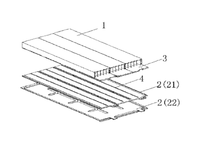
[0013] Optionally, the second electrically conductive layer has a thickness in
the
range of 0.1 tmto 50 p.m.
[00141 Optionally, the support layer is a thermoplastic elastomer layer with
pores.
0015]
Optionally, the current collector further includes a third electrically
conductive layer, having a grid structure distributed on the first surface or
the second
surface of the support layer.
[0016]
Optionally, the first electrically conductive layer is distributed on
the first
surface of the support layer, and the third electrically conductive layer is
distributed on the
second surface of the support layer.
[0017]
Optionally, the first electrically conductive layer is distributed on
the
second surface of the support layer, and the third electrically conductive
layer is distributed
on the first surface of the support layer.
[0018] Optionally, the second electrically conductive layer is provided on a
surface of the third electrically conductive layer away from the support
layer.
[0019]
Optionally, the first electrically conductive layer is a metal
component,
and the third electrically conductive layer is a metal component.
[0020] In a second aspect of the present disclosure, an electrode sheet is
provided.
The electrode sheet includes a current collector according to the first
aspect, and an
electrode slurry layer formed on the second electrically conductive layer.
0021] In a third aspect of the present disclosure, a preparation method for a
current collector is provided. The preparation method for a current collector
includes the
3
CA 03223411 2023- 12- 19
following steps:
providing a support layer;
forming a first electrically conductive layer on a first surface and/or a
second
surface of the support layer by at least one of press printing, printing,
deposition, and
magnetron sputtering, where the first electrically conductive layer has a grid
structure
distributed on the support layer;
forming a second electrically conductive layer on the whole surface of the
first
electrically conductive layer; and
drying the second electrically conductive layer, to solidify the second
electrically
conductive layer on the surface of the first electrically conductive layer, so
as to prepare
the current collector.
[0022]
One technical effect of the present disclosure is that a current
collector is
provided. The current collector includes a support layer, a first electrically
conductive layer
having a grid structure and a second electrically conductive layer formed on
the first
electrically conductive layer. By providing the support layer, the strength
requirement of
the current collector is met, and by the first electrically conductive layer
and the second
electrically conductive layer, the electrical conductivity of the current
collector is attained.
In the embodiment of the present disclosure, the first electrically conductive
layer has a
grid structure formed on the support layer, thus reducing the weight per unit
area of the
current collector, and improving the energy density of the battery. The first
electrically
conductive layer having a grid structure is formed on the support layer, the
current collector
as a whole can have a porous structure, and the porous current collector is
permeable to
ions in a direction perpendicular to the thickness of the current collector,
that is, the current
4
CA 03223411 2023- 12- 19
collector allows lithium ions to penetrate through, thus increasing the
application scenarios
of the current collector.
[0023] Other features and advantages of the present
disclosure will become
apparent from the following detailed description of exemplary embodiments of
the present
disclosure with reference to the drawings.
BRIEF DESCRIPTION OF THE DRAWINGS
[0024] Accompanying drawings that constitute a part of the specification show
embodiments of the present disclosure, and are used together with the
specification to
explain the principle of the present disclosure.
[0025] FIG. 1 shows a first schematic view of a current collector according to
the present disclosure.
[0026] FIG. 2 shows a second schematic view of a current collector according
to
the present disclosure.
[0027] FIG. 3 shows a third schematic view of a current collector according to
the present disclosure.
[0028] FIG. 4 shows a fourth schematic view of a current collector according
to
the present disclosure.
[0029] FIG. 5 shows a fifth schematic view of a current collector according to
the present disclosure.
[0030] FIG. 6 shows a sixth schematic view of a current collector according to
the present disclosure.
[0031] FIG. 7 shows a schematic structural view of a first electrically
conductive
5
CA 03223411 2023- 12- 19
layer according to the present disclosure.
[0032] FIG. 8 shows a flow chart of a preparation method for a current
collector
according to the present disclosure.
[0033] List of reference numerals:
[0034] 1. support layer; 11. first surface; 12. second surface; 2. first
electrically
conductive layer; 3. second electrically conductive layer; 4. third
electrically conductive
layer; 20. grid structure; 201. grid hole; 202. grid wall.
DETAILED DESCRIPTION
[0035] Various exemplary embodiments of the present disclosure are now be
described in detail with reference to the accompanying drawings. It is to be
noted that
unless otherwise specified, the relative arrangement, numerical expressions,
and numerical
values of components and steps described in the embodiments do not limit the
scope of the
disclosure.
[0036] The following descriptions of at least one exemplary embodiment are
merely illustrative, and do not constitute any limitation on the present
disclosure and
application or use thereof in any way.
[0037] Technologies, and devices known to those of ordinary skill in related
art
may not be discussed in detail, but where appropriate, the techniques and the
devices
should be considered as a part of the specification.
[0038] In all examples shown and discussed herein, any specific value should
be
construed to be merely exemplary, and not as limitations. Therefore, other
examples of
6
CA 03223411 2023- 12- 19
exemplary embodiments may have different values.
[0039] It should be noted that similar reference numerals and letters indicate
similar items in the following drawings. Therefore, once an item is defined in
a drawing, it
has no need to be discussed further in the following drawings.
[0040] Therefore, given the limited existing material systems at present,
efforts
are made to reduce the proportion of inactive components in the battery to
improve the
energy density of the battery in the industry. Porous current collector
technology is a key
technology to reduce the proportion of inactive components, and which can also
improve
the energy density of the battery. At present, the types of porous current
collectors include
foamed metal sheets, perforated metal foils, and carbon fiber sheets, etc. In
the existing
porous current collector technology, the foamed metal sheet has large
thickness and high
weight per unit area, reducing the specific energy density of the battery; and
the perforated
metal foil has the problem of high perforation cost. The strength of the
current collector
decreases seriously when the perforated hole is larger. Carbon fiber sheets,
such as carbon
fiber cloth, are brittle and expensive.
[0041] In view of the above technical problems in a first aspect of the
present
disclosure, a current collector is provided. As shown in FIGs. 1 to 3, the
current collector
includes: a support layer 1, a first electrically conductive layer 2 and a
second electrically
conductive layer 3.
[0042] The support layer 1 has a first surface 11 and a second surface 12
arranged
opposite to each other. The first electrically conductive layer 2 has a grid
structure 20
distributed on the first surface 11 and/or the second surface 12 of the
support layer 1. The
second electrically conductive layer 3 is provided on a surface of the first
electrically
7
CA 03223411 2023- 12- 19
conductive layer 2 away from the support layer 1.
[0043] In other words, the current collector mainly includes the support layer
1,
the first electrically conductive layer 2 and the second electrically
conductive layer 3. The
support layer 1 has structural strength, ensuring the strength of the current
collector to meet
the assembly requirement of the battery. Moreover, the support layer 1 has
pores, allowing
lithium ions to pass through. The first electrically conductive layer 2 is
formed on the
support layer 1, and the second electrically conductive layer 3 is formed on
the first
electrically conductive layer 2. The conductive layer is formed to have a grid
structure,
such that the current collector as a whole has a porous structure, allowing
lithium ions to
pass through, and ensuring the lithium ion transmission ability of the current
collector. The
porous current collector allows lithium ion to penetrate through in a
direction perpendicular
to its two-dimensional plane (that is, the thickness direction of the porous
current collector),
thus broadening the application scenarios. For example, the current collector
can be applied
to electrochemical lithium supplementation.
[0044] In an embodiment, as shown in FIG. 1, the first electrically conductive
layer 2 has a grid structure 20 distributed on the first surface 11 of the
support layer 1, the
second electrically conductive layer 3 is formed on the first electrically
conductive layer 2,
and no conductive layer is provided on the second surface 12 of the support
layer 1, to form
a first current collector. The first current collector only includes the
support layer 1, the
first electrically conductive layer 2 and the second electrically conductive
layer 3.
[0045] In another embodiment, as shown in FIG. 2, the first electrically
conductive layer 2 has a grid structure 20 distributed on the second surface
12 of the support
layer 1, the second electrically conductive layer 3 is formed on the first
electrically
8
CA 03223411 2023- 12- 19
conductive layer 2, and no conductive layer is provided on the first surface
11 of the support
layer 1, to form a first current collector. The structure of the first current
collector shown
in FIG. 2 differs from the structure of the first current collector shown in
FIG. 1 in that the
first electrically conductive layer 2 is provided on different surfaces of the
support layer 1.
[0046] In another embodiment, as shown in FIG. 3, the first electrically
conductive layer 2 has a grid structure 20 distributed on the first surface 11
and the second
surface 12 of the support layer 1, and the second electrically conductive
layer is formed on
the two first electrically conductive layers 2 respectively, to form a first
current collector.
The structure of the first current collector shown in FIG. 3 differs from the
structure of the
first current collector shown in FIGs. 1 and 2 in that in the first current
collector shown in
FIG. 3, the first electrically conductive layer 2 is formed on both the first
surface 11 and
the second surface 12 of the support layer 1; and in the first current
collector shown in FIGs.
1 and 2, the first electrically conductive layer 2 is merely formed on the
first surface 11 or
the second surface 12 of the support layer I.
[0047] In the embodiment of the present disclosure, the first electrically
conductive layer 2 has a grid structure 20 distributed on the support layer 1.
Since the first
electrically conductive layer 2 has a grid structure 20, lithium ions can
easily pass through
the grid holes of the grid structure 20. On the one hand, the grid structure
of the first
electrically conductive layer 2 ensures the normal penetration of lithium
ions; and on the
other hand, the grid structure 20 of the first electrically conductive layer 2
reduces the
weight per unit area of the current collector, thus improving the energy
density of the
battery and reducing the internal resistance of the current collector, to form
a larger current
for external output. The first electrically conductive layer 2 is electrically
conductive,
9
CA 03223411 2023- 12- 19
ensuring the electrical conductivity of the current collector. Therefore, the
first electrically
conductive layer 2 having a grid structure ensures the electron collection
ability and lithium
ion transmission ability of the current collector.
[0048] The second electrically conductive layer 3 is provided on a surface of
the
first electrically conductive layer 2 away from the support layer 1. The
second electrically
conductive layer 3 further improves the electronic conductivity of the current
collector
without hindering the penetration of lithium ions. Particularly, the second
electrically
conductive layer 3 is provided on the whole surface of the first electrically
conductive layer
2. The second electrically conductive layer 3 on a grid wall 202 cooperates
with the first
electrically conductive layer 2 (for example, the second electrically
conductive layer 3
covering the grid area makes up for the deficiency of the first electrically
conductive layer
2), to ensure the electron collection ability and lithium ion transmission
ability of the
current collector. Particularly, the third electrically conductive layer 3
collects electrons in
hollowed-out areas in the grid, without hindering the lithium ion
transmission.
[0049] The current collector according to the embodiment of the present
disclosure has high strength, light weight, good electrical conductivity, and
also a porous
structure, ensuring the normal transmission of lithium ions.
[0050] In an embodiment, the first electrically conductive layer 2 has a
thickness
in the range of 0.1 gm to 50 gm. Optionally, the first electrically conductive
layer 2 has a
thickness in the range of 1 gm-10 gm.
[0051] In an embodiment, the support layer 1 has a thickness in the range of
0.1
gm-20 gm. Optionally, the support layer 1 has a thickness in the range of 5 gm-
15 gm.
[0052] In an embodiment, the second electrically conductive layer 3 has a
CA 03223411 2023- 12- 19
thickness in the range of 0.1 um to 50 um. Optionally, the second electrically
conductive
layer 3 has a thickness in the range of 5 um-20 um.
[0053] In an embodiment, the current collector has a thickness in the range of
1
um to 100 um. Optionally, the current collector has a thickness in the range
of 15 um to 50
gm.
[0054]
Particularly, in this embodiment, the thickness of the first
electrically
conductive layer 2 is defined. Considering the overall electrical conductivity
and the ion
transmission performance of the current collector, the thickness of the first
electrically
conductive layer 2 is set in this range, which reduces the weight per unit
area of the current
collector, reduces the proportion of non-active materials, and improves the
energy density
of the battery, while the overall thickness of the current collector is not
affected.
[0055] In this embodiment, the thickness of the support layer 1 is defined. By
controlling the thickness of the support layer 1 in this range, the weight per
unit area of the
current collector is reduced, the proportion of non-active materials is
reduced, and the
energy density of the battery is improved when used in a battery, while the
overall strength
of the current collector is not affected.
[0056] In this embodiment, the thickness of the second electrically conductive
layer 3 is defined. The thickness of the second electrically conductive layer
3 affects the
assistance of the first electrically conductive layer 2 in the electron
collection ability and
the lithium ion transmission ability of the current collector. As the
thickness of the second
electrically conductive layer 3 decreases, the electron collection ability of
the current
collector decreases, and the lithium ion transmission ability increases; or
otherwise, the
electron collection ability of the current collector increases, and the
lithium ion
11
CA 03223411 2023- 12- 19
transmission ability decreases. In this embodiment, by controlling the
thickness of the
second electrically conductive layer 3 within this range, the normal electron
collection
ability and lithium ion transmission ability of the current collector can be
effectively
improved.
[0057] In this embodiment, the thickness of the support layer 1, the first
electrically conductive layer 2 and the second electrically conductive layer 3
is defined,
such that the thickness of the prepared current collector is defined within a
reasonable range.
In this embodiment, by defining the thickness of the current collector within
this range, the
overall electrical conductivity of the current collector is ensured on the one
hand; and on
the other hand, the proportion of non-active materials is reduced, ensuring
the energy
density of the battery.
[0058] In an embodiment, as shown in FIG. 7, the grid structure 20 includes
several grid holes 201 arranged into an array, and each of the grid hole 201
has an area in
the range of 0.01 cm2 to 100 cm2.
[0059] Further, particularly, the grid hole 201 is defined by grid walls 202,
and
the grid wall 202 has a wall thickness in the range of 0.1 mm to 50 mm.
[0060]
Particularly, the wall thickness of the grid wall 202 affects the
electrical
conductivity and the weight per unit area of the first electrically conductive
layer 2. To
balance the electrical conductivity of the first electrically conductive layer
2 and the weight
per unit area of the first electrically conductive layer 2, the wall thickness
of the grid wall
202 is defined in this embodiment. By defining the thickness of the grid wall
202 in this
range, the weight per unit area of the first electrically conductive layer 2
is reduced, and
the energy density of the battery is improved; and the electrical conductivity
of the current
12
CA 03223411 2023- 12- 19
collector is ensured.
[0061] In the embodiment, the grid structure includes several grid holes 201
arranged into an array, and the grid holes 201 are distributed on the support
layer 1 in the
form of an array. The grid hole 201 can be a rectangular hole, a round hole,
and a diamond
hole, etc. the shape of the grid hole 201 is not particularly limited in this
embodiment. In
the embodiment, each grid hole 201 has an area in the range of 0.01 cm2 to 100
cm2.
Optionally, each grid hole 201 has an area in the range of 1 cm2 to 10 cm2.
[0062]
Particularly, the area of the grid hole 201 affects the electrical
conductivity of the first electrically conductive layer 2 and the weight per
unit area of the
current collector. To balance the electrical conductivity of the first
electrically conductive
layer 2 and the weight per unit area of the first electrically conductive
layer 2, the area of
the grid hole 201 is defined in this embodiment. Studies show that by defining
the area of
the grid hole 201 in this range, the weight per unit area of the first
electrically conductive
layer 2 is reduced, the energy density of the battery is improved, and the
electrical
conductivity of the current collector is ensured.
[0063] In an embodiment, the support layer 1 is a thermoplastic elastomer
layer
with pores.
[0064]
Particularly, the support layer 1 is a substrate, the first electrically
conductive layer 2 is formed on the support layer 1, and the second
electrically conductive
layer 3 is formed on the first electrically conductive layer 2. The support
layer 1 is a
thermoplastic elastomer layer with pores. For example, pores are formed on the
support
layer 1, where the diameter of the pores is less than 100 pm.
[0065] In this embodiment, the support layer 1 is a thermoplastic elastomer
layer
13
CA 03223411 2023- 12- 19
with pores, to improve the structural strength of the current collector.
[0066]
Particularly, the thermoplastic elastomer layer is specifically one of a
polyolefin thermoplastic elastic layer, a polyurethane thermoplastic elastic
layer or a
polyamide thermoplastic elastic layer. The support layer 1 can also be a
composite film
layer, which is formed by physically pressing at least two of a polyolefin
thermoplastic
elastic layer, a polyurethane thermoplastic elastic layer or a polyamide
thermoplastic elastic
layer.
[0067] In a specific embodiment, the material of the support layer 1 is the
same
as that of the separator of the lithium battery, thus ensuring the strength of
the current
collector, meeting the requirements in battery production, and ensuring the
normal
penetration of lithium ions.
[0068] In an embodiment, the first electrically conductive layer 2 having a
grid
structure is formed on the surface of the support layer 1 by deposition.
[0069] In an embodiment, the second electrically conductive layer 3 includes a
conductive agent and a binder. The conductive agent and the binder are mixed
uniformly
and then applied to the surface of the first electrically conductive layer 2
to form the second
electrically conductive layer 3.
[0070] Particularly, the conductive agent is one of carbon black, carbon
nanotubes or graphene. The binder is an electrically conductive binder, and
the binder is
specifically a polyvinylidene fluoride (PVDF) binder, a
polytetrafluoroethylene (PTFE)
binder, a carboxymethyl cellulose (CMC) binder or a styrene-butadiene rubber
(SBR)
binder.
[0071] The binder is mixed with the conductive agent at a weight ratio of
14
CA 03223411 2023- 12- 19
0.5:99.5 to 50:50,a solvent (NMP, water, and so on) is added to prepare a
slurry, and then
the slurry is coated on the surface of the first electrically conductive layer
2 to form the
second electrically conductive layer 3.
[0072] In an embodiment, as shown in FIGs. 4 to 6, the current collector
further
includes a third electrically conductive layer 4. The third electrically
conductive layer 4
has a grid structure 20 distributed on the first surface 11 or the second
surface 12 of the
support layer 1.
[0073]
The first electrically conductive layer 2 is distributed on the first
surface
11 of the support layer 1, and the third electrically conductive layer 4 is
distributed on the
second surface 12 of the support layer 1. Alternatively, the first
electrically conductive layer
2 is distributed on the second surface 12 of the support layer 1, and the
third electrically
conductive layer 4 is distributed on the first surface 11 of the support layer
1. The third
electrically conductive layer 4 has a grid structure 20 distributed on the
first surface 11 or
the second surface 12 of the support layer 1, and the second electrically
conductive layer 3
is provided on a surface of the third electrically conductive layer 4 away
from the support
layer 1.
[0074]
Particularly, the current collector further includes the third
electrically
conductive layer 4. In an embodiment, the third electrically conductive layer
4 has a grid
structure 20 distributed on the first surface 11 of the support layer 1. In
another embodiment,
the third electrically conductive layer 4 has a grid structure 20 distributed
on the second
surface 12 of the support layer 1.
[0075]
As shown in FIG. 6, the third electrically conductive layer 4 is
distributed
on the first surface 11 of the support layer 1, the first electrically
conductive layer 2 is
CA 03223411 2023- 12- 19
distributed on the second surface 12 of the support layer 1, and the second
electrically
conductive layer 3 is formed respectively on the surface of the first
electrically conductive
layer 2 and the surface of the third electrically conductive layer 4, to form
a third current
collector. The third current collector includes the support layer 1, the first
electrically
conductive layer 2, the second electrically conductive layer 3 and the third
electrically
conductive layer 4.
[0076] Alternatively, in an embodiment, the third electrically conductive
layer 4
is distributed on the second surface 12 of the support layer 1, the first
electrically
conductive layer 2 is distributed on the first surface 11 of the support layer
1, and the second
electrically conductive layer 3 is formed respectively on the surface of the
first electrically
conductive layer 2 and the surface of the third electrically conductive layer
4, to form a
third current collector.
[0077]
As shown in FIG. 6, the first electrically conductive layer 2 is
distributed
on the second surface 12 of the support layer 1, and the third electrically
conductive layer
4 is distributed on the first surface 11 of the support layer 1. In this case,
the current
collector is respectively applied with a positive or a negative electrode
slurry on two
surfaces, and then cut, for use as a battery core.
[0078] Alternatively, in an embodiment, as shown in FIG. 4, the third
electrically
conductive layer 4 has a grid structure 20 distributed on the first surface 11
of the support
layer 1, the second electrically conductive layer 3 is formed on the surface
of the third
electrically conductive layer 4, and no conductive layer is provided on the
second surface
12 of the support layer 1, to form a second current collector. The second
current collector
only includes the support layer 1, the third electrically conductive layer 4
and the second
16
CA 03223411 2023- 12- 19
electrically conductive layer 3.
[0079] In another embodiment, as shown in FIG. 5, the third electrically
conductive layer 4 has a grid structure 20 distributed on the second surface
12 of the support
layer 1, the second electrically conductive layer 3 is formed on the surface
of the third
electrically conductive layer 4, and no conductive layer is provided on the
first surface 11
of the support layer 1, to form a second current collector.
[0080] In another embodiment, the third electrically conductive layer 4 has a
grid
structure 20 distributed on the first surface 11 and the second surface 12 of
the support
layer 1, and the second electrically conductive layer 3 is formed respectively
on the
surfaces of the two third electrically conductive layers 4, to form a second
current collector.
[0081]
In a specific embodiment, the first electrically conductive layer 2 is a
positive electrode conductive layer, and the third electrically conductive
layer 4 is a
negative electrode conductive layer. Particularly, the support layer 1 is only
ionically
conductive and not electronically conductive, and can be regarded as a
separator of the
battery. The first electrically conductive layer 2 is a positive electrode
conductive layer
located on one side of the support layer 1, and the third electrically
conductive layer 4 is a
negative electrode conductive layer located on another side of the support
layer 1.
Alternatively, the first electrically conductive layer 2 is a negative
electrode conductive
layer, and the third electrically conductive layer 4 is a positive electrode
conductive layer.
In this embodiment, description is made by way of examples where the first
electrically
conductive layer 2 is a positive electrode conductive layer, and the third
electrically
conductive layer 4 is a negative electrode conductive layer. For example, the
positive
electrode conductive layer is an aluminum grid structure, and the negative
electrode
17
CA 03223411 2023- 12- 19
conductive layer is a copper grid structure.
[0082] In an embodiment, the positive electrode conductive layer is
distributed
on the first surface 11 of the support layer 1, and the second electrically
conductive layer 3
is formed on the positive electrode conductive layer, to form a positive
electrode current
collector. Alternatively, the positive electrode conductive layer is
distributed on the second
surface 12 of the support layer 1, and the second electrically conductive
layer 3 is formed
on the positive electrode conductive layer, to form a positive electrode
current collector.
Alternatively, the positive electrode conductive layer is distributed on the
first surface 11
and the second surface 12 of the support layer 1, and the second electrically
conductive
layer 3 is formed on the positive electrode conductive layer to form a
positive electrode
current collector. That is, the current collector is a positive electrode
current collector.
[0083] In an embodiment, the negative electrode conductive layer is
distributed
on the first surface 11 of the support layer 1, and the second electrically
conductive layer 3
is formed on the negative electrode conductive layer, to form a negative
electrode current
collector. Alternatively, the negative electrode conductive layer is
distributed on the second
surface 12 of the support layer 1, and the second electrically conductive
layer 3 is formed
on the negative electrode conductive layer, to form a negative electrode
current collector.
Alternatively, the negative electrode conductive layer is distributed on the
first surface 11
and the second surface 12 of the support layer 1, and the second electrically
conductive
layer 3 is formed on the negative electrode conductive layer, to form a
negative electrode
current collector. That is, the second current collector is a negative
electrode current
collector.
[0084] In an embodiment, the support layer 1 is only ionically conductive and
18
CA 03223411 2023- 12- 19
not electronically conductive, and can be regarded as a separator of the
battery. The first
electrically conductive layer 2 is a positive electrode conductive layer
located on one side
of the support layer 1, and the third electrically conductive layer 4 is a
negative electrode
conductive layer located on another side of the support layer 1. For example,
the positive
electrode conductive layer is distributed on the first surface 11 of the
support layer 1, and
the second electrically conductive layer 3 is formed on the positive electrode
conductive
layer; and at the same time, the negative electrode conductive layer is
distributed on the
second surface 12 of the support layer 1, and the second electrically
conductive layer 3 is
formed on the negative electrode conductive layer, to from a third current
collector. That
is, the third current collector is a structure integrated with the positive
electrode current
collector and the negative electrode current collector.
[0085] In an embodiment, the first electrically conductive layer 2 is a metal
component, and the third electrically conductive layer 4 is a metal component.
[0086]
Particularly, the first electrically conductive layer 2 and the third
electrically conductive layer 4 are both metal grid components. The first
electrically
conductive layer 2 can be a positive electrode conductive layer, and the third
electrically
conductive layer 4 can be a negative electrode conductive layer.
Alternatively, the first
electrically conductive layer 2 can be a negative electrode conductive layer,
and the third
electrically conductive layer 4 can be a positive electrode conductive layer.
[0087] When the first
electrically conductive layer 2 is a positive electrode
conductive layer, the first electrically conductive layer 2 is an aluminum
component. For
example, the first electrically conductive layer 2 having a grid structure 20
is formed by an
aluminum component.
19
CA 03223411 2023- 12- 19
[0088] When the third electrically conductive layer 4 is a negative electrode
conductive layer, the third electrically conductive layer 4 is a copper
component. For
example, the third electrically conductive layer 4 having a grid structure 20
is formed by a
copper component.
[0089] In the lithium ion battery, the positive electrode has a high
potential. The
oxide layer of aluminum is relatively dense, and can prevent the oxidation of
the current
collector. Copper will undergo lithium intercalation at a high potential, and
is suitably not
used as a positive electrode conductive layer. Therefore, the positive
electrode conductive
layer is generally an aluminum foil. The negative electrode has a low
potential, and
aluminum tends to form a Al-Li alloy at a low potential. Therefore, the
negative electrode
conductive layer is generally a copper foil. The copper foil and aluminum foil
are not
interchangeable.
[0090] In a second aspect of the present disclosure, an electrode sheet is
provided.
The electrode sheet includes a current collector according to the first
aspect, and an
electrode slurry layer. The electrode slurry layer is formed on the second
electrically
conductive layer 3. For example, the electrode slurry layer is coated or
sprayed on the
second electrically conductive layer 3. The electrode sheet includes a
positive electrode
sheet and a negative electrode sheet.
[0091] In an embodiment, the electrode slurry layer includes an electrode
active
material, a conductive agent, and a binder. The active material is a positive
electrode active
material or a negative electrode active material for use in a battery. For
example, the
positive electrode active material includes one of lithium cobalt oxide,
lithium manganese
oxide, lithium iron phosphate and a ternary material, etc. The negative
electrode active
CA 03223411 2023- 12- 19
material includes a carbon material. For example, the negative electrode
active material is
graphite. For example, the conductive agent includes one of carbon black,
carbon
nanotubes or graphene. For example, the binder is an electrically conductive
binder. For
example, the binder is a polyvinylidene fluoride (PVDF) binder, a
polytetrafluoroethylene
(PTFE) binder, a carboxymethyl cellulose (CMC) binder, or a styrene-butadiene
rubber
(SBR) binder.
[0092] In an embodiment, the first electrically conductive layer 2 is
distributed
on the first surface 11 and/or the second surface 12 of the support layer 1,
and the second
electrically conductive layer 3 is formed on the first electrically conductive
layer 2, to form
a first current collector. A positive electrode slurry layer is provided on
the first current
collector to form a first electrode sheet. That is, the first electrode sheet
is a positive
electrode sheet.
[0093] In an embodiment, the third electrically conductive layer 4 is
distributed
on the first surface 11 and/or the second surface 12 of the support layer 1,
and the second
electrically conductive layer 3 is formed on the surface of the third
electrically conductive
layer 4, to form a second current collector. A negative electrode slurry layer
is provided on
the second current collector to form a second electrode sheet. That is, the
second electrode
sheet is a negative electrode sheet.
[0094] In an embodiment, the first electrically conductive layer 2 is
distributed
on the first surface 11 of the support layer 1, the second electrically
conductive layer 3 is
provided on the first electrically conductive layer 2, and a positive
electrode slurry layer is
provided on the second electrically conductive layer 3; and the third
electrically conductive
layer 4 is distributed on the second surface 12 of the support layer 1, the
second electrically
21
CA 03223411 2023- 12- 19
conductive layer 3 is formed on the third electrically conductive layer 4, and
a negative
electrode slurry layer is formed on the second electrically conductive layer
3, such that the
positive electrode sheet and the negative electrode sheet are integrated. The
structure
integrating the positive electrode sheet and the negative electrode sheet is
defined as a third
electrode sheet. In the third electrode sheet, the support layer corresponds
to a separator
structure in a battery, and the support layer is only ionically conductive and
not
electronically conductive.
[0095] In an embodiment, a battery core is provided. The battery core includes
a positive electrode sheet, a negative electrode sheet, and a separator
provided between the
positive electrode sheet and the negative electrode sheet. When the positive
electrode sheet
and the negative electrode sheet are separate structures, the positive
electrode sheet, the
separator, and the negative electrode sheet are wound into the battery core.
Alternatively,
the active material layer of a single-sided positive electrode sheet is
attached to a surface
of the support layer 1 in a single-sided negative electrode sheet, and wound
into the battery
core. In this embodiment, the thickness of the current collector of the
battery core is further
reduced, and the energy density of the battery is improved.
[0096] When the positive electrode sheet and the negative electrode sheet are
integrated into one piece, the battery core includes multiple third electrode
sheets, and a
separator is provided between adjacent third electrode sheets.
[0097] In a third aspect of the present disclosure, a preparation method for a
current collector is provided. As shown in FIG. 8, the preparation method for
a current
collector includes the following steps:
S101: providing a support layer 1;
22
CA 03223411 2023- 12- 19
S102: forming a first electrically conductive layer 2 on a first surface 11
and/or a
second surface 12 of the support layer 1 by at least one of press printing,
printing,
deposition, and magnetron sputtering, where the first electrically conductive
layer 2 has a
grid structure 20 distributed on the support layer 1;
S 103: applying a slurry on the whole surface of the first electrically
conductive
layer 2 to form a second electrically conductive layer 3; and
S104: drying the second electrically conductive layer 3, to solidify the
second
electrically conductive layer 3 on the surface of the first electrically
conductive layer 2, so
as to prepare the current collector.
[0098] Particularly, the support layer 1 is a thermoplastic elastomer layer
with
pores, to improve the structural strength of the current collector.
[0099]
Particularly, the thermoplastic elastomer layer is specifically at least
one
of a polyolefin thermoplastic elastic layer, a polyurethane thermoplastic
elastic layer or a
polyamide thermoplastic elastic layer. The support layer 1 can also be a
composite film
layer, which is formed by physically pressing at least two of a polyolefin
thermoplastic
elastic layer, a polyurethane thermoplastic elastic layer or a polyamide
thermoplastic elastic
layer.
[0100] In a specific embodiment, the material of the support layer 1 is the
same
as that of the separator of the lithium battery, thus ensuring the strength of
the current
collector, meeting the requirements in battery production, and ensuring the
normal
penetration of lithium ions.
[0101]
In Step S102, the first electrically conductive layer 2 is printed on
the
support layer 1, for example, by screen printing. Alternatively, the first
electrically
23
CA 03223411 2023- 12- 19
conductive layer 2 is printed on the support layer 1 by 3D printing.
Alternatively, the first
electrically conductive layer 2 is formed on the support layer 1 by deposition
or the first
electrically conductive layer 2 is formed on the support layer 1 by magnetron
sputtering.
[0102] In a specific embodiment, the first electrically conductive layer 2 can
be
attained by the following processes:
[0103] 1) A grid structure 20 is printed on the support
layer 1, and then a metal
grid structure is formed by at least one of physical vapor deposition,
chemical vapor
deposition, electrochemical deposition and magnetron sputtering; and the first
electrically
conductive layer 2 is cleaned, and dried.
[0104] 2) The first electrically conductive layer 2 is directly formed on
the
support layer 1 by printing or 3D printing and dried.
[0105] 3) A grid structure 20 is printed on the support layer 1, and a metal
layer
is electroplated on the grid structure 20, then washed, and dried. The
electroplated metal
layer acts to increase the electrical conductivity of the first electrically
conductive layer 2.
[0106] Notably, in this embodiment, the process of forming the first
electrically
conductive layer on the support layer 1 is not particularly limited, as long
as the formed
first electrically conductive layer 2 has a grid structure 20, and the
thickness and the grid
size of the first electrically conductive layer 2 are met. The third
electrically conductive
layer 4 is formed on the support layer 1 in the same way as that for the first
electrically
conductive layer 2.
[0107] In Step 103, the second electrically conductive layer 3 can be formed
on
the first electrically conductive layer 2 by spraying or coating. The
formation of the second
electrically conductive layer 3 by spraying or coating facilitates the control
of the thickness
24
CA 03223411 2023- 12- 19
of the second electrically conductive layer 3.
[0108] In Step 104, before drying the second electrically conductive layer 3,
the
second electrically conductive layer 3 is rolled, to ensure the flatness of
the second
electrically conductive layer 3. For example, the second electrically
conductive layer 3 on
the surface of the first electrically conductive layer 2 can be solidified by
maintaining at
100 to 150 C for 5-12 hrs.
[0109] An embodiment of the present disclosure provides a current collector.
The current collector includes a support layer 1, a first electrically
conductive layer 2
having a grid structure 20 and a second electrically conductive layer 3 formed
on the first
electrically conductive layer 2. By providing the support layer 1, the
strength requirement
of the current collector is met, and by the first electrically conductive
layer 2 and the second
electrically conductive layer 3, the electrical conductivity of the current
collector is attained.
In the embodiment of the present disclosure, the first electrically conductive
layer 2 has a
grid structure 20 formed on the support layer 1, thus reducing the weight per
unit area of
the current collector, and improving the energy density of the battery.
[0110] The performance of the current collector prepared in this embodiment
and the performance of a battery prepared with the current collector are
verified by way of
specific examples.
[0111] Example 1
[0112] 1) Grids were printed on a first surface 11 and a second surface 12
of a 5
pm-thick polypropylene support layer (the printing slurry was prepared by
adding water to
CMC and silica mixed at a weight ratio of 1:9, and the grids were dried after
printing).
Aluminum is deposited on the support layer printed with grids by physical
vapor deposition,
CA 03223411 2023- 12- 19
cleaned (the grids printed on the support layer wound be dissolved, and
removed in the
cleaning process), and dried, to form a first electrically conductive layer 2.
The thickness
of deposited aluminum is 5 p,m, the grid hole is a square with a side length
of 1 cm, and
the spacing is 1 mm.
1_0113] NMP was added to PVDF and carbon nanotubes mixed at a weight ratio
of 5:95 to prepare a uniform slurry, and the slurry was coated on the two
first electrically
conductive layers, to form a second electrically conductive layer on the first
electrically
conductive layer. After drying and rolling, a porous current collector was
obtained. The
porous current collector is a positive electrode current collector designated
as Sl.
[0114] Lithium iron phosphate, PVDF, carbon nanotubes, and carbon black were
mixed at a weight ratio of 95:2:1.5:1.5, to which NMP was added to prepare a
positive
electrode slurry. The positive electrode slurry was coated on the second
electrically
conductive layer, dried, rolled, and cut to form a positive electrode sheet.
The positive
electrode sheet has an areal density of 200 g/m2.
[0115] 2) Grids were printed on a first surface 11 and a second surface 12 of
a 5
gm-thick polypropylene support layer (the printing slurry was prepared by
adding water to
CMC and silica mixed at a weight ratio of 1:9, and the grids were dried after
printing).
Copper is deposited on the support layer 1 printed with grids by physical
vapor deposition,
cleaned, and dried, to form a first electrically conductive layer 2. The
thickness of deposited
copper is 5 gm, the grid hole is a square with a side length of 1 cm, and the
spacing is 1
mm.
[0116] NMP was added to PVDF and carbon nanotubes mixed at a weight ratio
of 5:95 to prepare a uniform slurry, and the slurry was coated on the two
first electrically
26
CA 03223411 2023- 12- 19
conductive layers, to form a second electrically conductive layer on the first
electrically
conductive layer. After drying and rolling, a porous current collector was
obtained. The
porous current collector is a negative electrode current collector designated
as S2.
[0117] Graphite CMC, carbon nanotubes, and carbon black were mixed at a
weight ratio of 95:2:1.5:1.5, to which NMP was added to prepare a negative
electrode slurry.
The negative electrode slurry was coated on the second electrically conductive
layer, dried,
rolled, and cut to form a negative electrode sheet. The negative electrode
sheet has an areal
density of 90 g/m2.
[0118] 3) A pouch battery of 6.1 cm*7.2 cm was prepared with the positive
electrode sheet and the negative electrode sheet above, in which the amount of
electrolyte
solution injected was 2 mL. After infiltration, formation, aging, and capacity
grading, The
battery was subjected to charging and discharging test at 0.5C.
[0119] Comparative Example 1
[0120] Lithium iron phosphate, PVDF, carbon nanotubes, and carbon black were
mixed at a weight ratio of 95:2:1.5:1.5, to which NMP was added to prepare a
positive
electrode slurry. The positive electrode slurry was coated on a 10 Rm-thick
aluminum foil
current collector D1, dried, rolled, and cut to form a positive electrode
sheet. The positive
electrode sheet has an areal density of 200 g/m2.
[0121] Graphite CMC, carbon nanotubes, and carbon black were mixed at a
weight ratio of 95:2:1.5:1.5, to which water was added to prepare a slurry.
The slurry was
coated on a 10 lim-thick copper foil current collector D2, dried, rolled, and
cut to form a
negative electrode sheet. The negative electrode sheet has an areal density of
90 g/m2.
[0122] A pouch battery of 6.1 cm*7.2 cm was prepared with the above electrode
27
CA 03223411 2023- 12- 19
sheets, in which the amount of electrolyte solution injected was 2 mL. After
infiltration,
formation, aging, and capacity grading, the battery was subjected to charging
and
discharging test at 0.5C.
[0123] The current collectors Sl, S2, D1, and D2 were weighed respectively,
and
the weight per unit area was calculated. Each battery was constant-current
charged to 3.8
V at 0.5C at room temperature, and then the discharging capacity and charging
capacity of
the battery were recorded.
Current collector Weight per unit area/g/m2
First discharge capacity/mAh
Si 4
100
S2 10
D1 41
102
D2 73
[0124] It is found through comparison that the weight per unit area of the
current
collector prepared in the present disclosure is only 10-15% of the weight per
unit area of
the current collector used in the related art, so the weight proportion of the
current collector
in battery is greatly reduced. Moreover, the current collector has good
performance, and
the battery capacity is up to 98% or higher of the conventional current
collector.
[0125] In the above embodiments, the differences between the various
embodiments are mainly described. Where not contradictory, the different
optimal features
of various embodiments can be combined to form a more preferred embodiment,
which
will not be detailed here, considering the brevity of description.
[0126] Although some specific embodiments of the present disclosure have been
described in detail by way of examples, a person skilled in the art should
understand that
the foregoing examples are merely provided for description, and not intended
to limit the
28
CA 03223411 2023- 12- 19
scope of the present disclosure. A person skilled in the art should appreciate
that
modifications can be made to the foregoing embodiments without departing from
the scope
and spirit of the present disclosure. The scope of the present disclosure is
defined by the
appended claims.
29
CA 03223411 2023- 12- 19