Note: Descriptions are shown in the official language in which they were submitted.
LOW POWER DUAL-SENSITIVITY FG-MOSFET SENSOR FOR A WIRELESS
RADIATION DOSIMETER
[0001] The present application is a divisional application of
Canadian Patent No.
3,093,736 Filed September 15 2020.
1. FIELD OF THE INVENTION
[0002] The present invention relates generally to medical sensors,
and more particularly,
to a low power floating gate metal-oxide semiconductor field-effect transistor
(FG-MOSFET) for
use in a wireless dosimeter tag for biomedical applications, such as for
determination of a
radiation dosage.
2. DESCRIPTION OF RELATED ART
[0003] The global market for medical sensors has experienced
significant growth in
recent years and is expected to continue growing at an accelerated rate. In
fact, the global
market demand for medical sensors is expected to increase more than 50% by the
year 2016
compared to 2006. This trend can be attributed to both constant innovation in
sensor system
design and the proliferation of novel applications for sensors, including X-
ray imaging and
radiation dosimetry. The latter category refers to sensors which measure X-ray
and gamma
radiation, also known as ionizing radiation. These sensors are used in a
variety of critical
procedures, including radiotherapy for cancer treatment and blood irradiation
for sterilization. In
an effort to minimize costs, the medical industry has expressed growing
interest over the use of
inexpensive, silicon-based, multi-sensitivity radiation dosimeters, thus
defining a new pathway
for research in this area to meet the set forth requirements.
1
Date Recue/Date Received 2023-12-27
[0004] Recent research initiatives for biomedical applications have
addressed the design
of flexible and wearable medical devices for early disease detection and
prevention health
monitoring and reduction of invasive medical procedures. This has created an
increasing
demand for flexible, conformal, compact, low-power wireless power transfer
(WPT) modules
.. that are easy to fabricate, low-cost and maintain efficient performance on
diverse host structures.
A number of sensors having a variety of functionalities for the targeted
application have been
reported in the prior art. These include passive and active circuit designs.
[0005] For example, US Patent Application, US2010/0096556A1 to Langis
Roy et al.,
incorporated herein by reference it its entirety, discloses a miniaturized
floating gate metal-oxide
semiconductor field-effect transistor (FG-MOSFET) radiation sensor. The sensor
preferably
comprises a matched pair of sensor and reference FG-MOSFETs wherein the sensor
FG-
MOSFET has a larger area floating gate with an extension over a field oxide
layer, for
accumulation of charge and increased sensitivity.
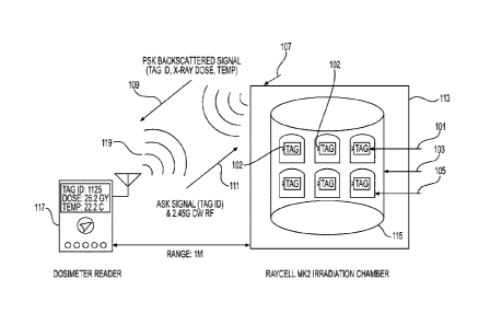
[0006] Several patents have been issued on color changing indicators,
monitors,
detectors, and dosimeters for monitoring a variety of biomedical processes.
For example, US
patent application, US 2011/0168920 Al to Yoder et al. discloses a device
comprising a
dosimeter for measuring one or more doses of radiation; and an RFID tag
comprising an antenna
for communicating with an RFID tag reader and non-volatile memory for storing
data therein.
This disclosure utilizes an optically stimulated luminescence (OSL) sensor
that includes a
reference filter material and is used to adjust the dose determined by the
reference sensor at very
low energies of x-rays or gamma rays.
[0007] For example, U.S. Patent No. 7,652,268 to Patel et al.
discloses a general purpose
dosimeter reader for determination of a radiation dosage, based on comparison
of an image of a
2
Date Recue/Date Received 2023-12-27
treated dosimeter with a series of images of a pre-treated dosimeter. The
dosimeter undergoes a
color change proportional to the dosage. The sensor may have more than one
indicator of the
same or different classes. The color change may be a gradual color development
or
intensification; a gradual color fading: a gradual color change or an abrupt
color change.
[0008] For example, U.S. Patent Application US2015/0116093A1 to Swager
discloses a
method of detecting a stimulus that can include detecting an output from a
radio frequency
identification tag including a sensor. The sensor portion is configured to
change resistivity when
the stimulus contacts or interacts with the radio frequency identification
tag, whereby the
resistivity change alters the output of the radio frequency identification
tag, wherein the radio
frequency identification tag includes a carbon nanotube or multiple carbon
nanotubes.
[0009] For example, the French Patent Application, FR2945128A1
discloses a dosimeter
for use during a radiotherapy treatment session, which has a printed circuit
board wrapped in an
envelope forming material, and a metal-oxide semiconductor field-effect
transistor (MOSFET)
placed on a printed circuit board. A RFID (radiofrequency identification
device) to identify the
dosimeter using an electronic device such as a memory chip containing data and
capable of using
an antenna to transmit information to a reader is also disclosed. The RFID
device may be
integrated to the printed circuit board or retrofitted thereon.
[0010] One area where such low-power wireless power transfer (WPT)
modules may be
beneficial is the preparation of blood products for medical applications, such
as to prevent the
transfusion-associated graft versus host disease (TA-GvHD), where it is
imperative that the
blood products are irradiated using X-ray or gamma ray sources. The current
radiation
measurement technology for each blood bag typically relies on radiation
sensitive paper tags
affixed to each bag that change color when exposed to radiation. The color
intensity of the tag
3
Date Recue/Date Received 2023-12-27
indicator corresponds with the radiation duration of which an allowed
radiation dose or deposit is
typically up to 50 Gray (Gy) of radiation in each blood bag. Using the visual
observation of the
shade of the color of the tag to deduce the cumulative radiation dose
delivered to a blood bag can
lead to an erroneous or inaccurate reading or result in that it is typically
prone to human
judgment. Therefore, a blood bag that has received, based on such visual
observation of the
paper tag, above the allowed dose, such as 50 Gy, must be discarded, even
though in actuality it
may have actually received a radiation dose of 50 Gy or less, resulting in a
serious wastage of
blood products.
[0011] Presently, blood products are irradiated in chambers using X-
ray or gamma-ray
sources to prevent transfusion associated graft versus host disease (TA-GvHD).
Typically, blood
product irradiation is identified using radiation-sensitive color indicators
known as RadTags.
Once applied to the blood bags, these labels give positive, visual
verification of irradiation
provided when a minimum of 25 gray (Gy) has been received. For example, after
irradiation, a
human operator visually checks the color on each tag to verify that the blood
is sufficiently
irradiated. However, this non-quantitative approach makes it difficult for a
human operator to
ascertain whether or not the blood in the blood bag under irradiation has
received over 50 Gy, a
maximum recommended dosage, thereby resulting in operational and cost
inefficiencies.
Currently available dosimeters cannot easily be integrated onto integrated
circuits (ICs) for
automatic readout; therefore, where many blood bags are being irradiated, it
takes time to
process all the bags and precision is lost as the operator gets tired.
Moreover, RadTags are not
reusable, hence increasing the cost of blood sterilization when large
quantities are involved.
[0012] Generally in FG-MOSFET devices ionizing radiation sensing by
floating gate
MOS involves pre-charging and sensing of a floating gate MOS sensor. Initially
the floating
4
Date Recue/Date Received 2023-12-27
gate is pre-charged with excess charge using a series of negative pulses from
an external source.
Ionizing irradiation creates electron-hole pairs inside the thick oxide layer
formed under the
floating gate extension. The generated electrons and holes are separated from
each other due to
the electric field that exists within the deep oxide formation. The electrons
from the floating gate
recombine with the generated holes that are attracted to them or in another
mechanism the excess
electrons on the floating gate receive enough energy from the incident X-ray
photons so that they
could escape the floating gate. Moreover, the dielectric layer on top of and
around the floating
gate extension contributes holes generated by ionizing radiation, which in
turn recombine with
the excess electrons. These mechanisms cause a reduction of charge inside the
floating gate
which is reflected in the output current. By sensing this change in the
current value, the
cumulative incident radiation on the device can be determined.
[0013] However, previous dosimeter designs have been implemented in
an older (thick
oxide) CMOS process which is ideal for dosimeter sensitivity, but generally
not typically-suited
to any form of RF wireless readout, although the thicker oxide can facilitate
prevention of charge
leakage out of the floating gate. Moreover, on the other hand, as the gate-
oxide thickness
reduces, the MOSFET typically becomes less sensitive to radiation. Also
challenges are present
in the use of a FG-MOSFET as a radiation sensor in relation to physical
parameters that can
significantly alter the FG-MOSFET's performance, particularly its sensitivity.
[0014] Also, as to other concerns, as holes pile up in oxide traps
during irradiation, the
space charge alters the oxide electric field which can typically decrease the
yield (increasing the
recombination of generated charge), leading to a sub-linear (less sensitive)
response. Further, as
more space charge accumulates in the oxide with increased dosage, the low-
field area in oxide
starts to expand towards the silicon and the trapped-hole distribution becomes
more restricted to
5
Date Recue/Date Received 2023-12-27
the area near the silicon/silicon dioxide (Si/Si02) interface, typically
resulting in sensitivity being
lost beyond this point. Moreover, a further concern is that MOS
characteristics are typically not
stable with time, commonly referred to as fading, as can be undesirable if the
irradiation result
measured is to be accessed over a relatively long period of time. Finally,
previous dosimeter
designs have typically exhibited only a single, fixed value of sensitivity,
which is generally
tailored to a single, specific application.
[0015] It is evident from the current state of art that while a FG-
MOSFET radiation
sensor can be used to measure irradiation, such FG-MOSFET sensors typically
have the
aforementioned drawbacks and limitations that are not particularly suitable
for a wireless
dosimeter and wireless dosimeter radiation measurements that may require
variable sensitivity.
[0016] Also, it would be desirable to replace the conventional
radiation tags with their
limitations, as discussed, by providing a FG-MOSFET radiation sensor that can
accurately
measure the cumulative dose of radiation a substance or object received, such
as received by
blood bags, and provide methods for realizing such FG-MOSFET radiation sensor
for use as
dosimeters.
[0017] What is needed is a FG-MOSFET sensor for use in a wireless
radiation dosimeter
formed of a thin-oxide that can be integrally formed on an integrated circuit
chip, such as for
measuring X-rays or other radiation that can accurately quantify the measured
radiation, such as
the irradiation level of blood.
[0018] Further, what is needed is a wireless radiation dosimeter that can
be fabricated as
a low cost semiconductor device, using a commercially available low cost
semiconductor
process, and that addresses limitations in the currently used technology for
radiation
6
Date Recue/Date Received 2023-12-27
measurement, such as wastage of blood, handling errors, and uncertainties of
the exact radiation
dose received, such as an X-ray dose received.
[0019] Also, what is also needed is a FG-MOSFET radiation sensor for
use in
conjunction with a wireless dosimeter formed on an integrated circuit chip
that facilitates
.. providing sensitivity to radiation energies, accuracy in radiation
measurements, and reduced
fading in relation to MOS characteristics to be able to maintain the charge
pre-irradiation and
post-irradiation, such as for measuring the irradiation of blood products.
[0020] In this regard, what is needed is a FG-MOSFET radiation sensor
in RF-CMOS
technology for use in a monolithically integrated radiation dosimeter, such as
for measuring X-
Ray radiation, with wireless readout capability and that can be manufactured
using commercially
available, low-cost radio-frequency complementary metal-oxide semi-conductor
(RF-CMOS)
processes, such as a 0.13 gm RF-CMOS process, desirably with a thin oxide
structure for a
monolithically integrated radiation sensor for use in wireless dosimetry.
[0021] Therefore, in view of the foregoing, it would be desirable to
have a FG-MOSFET
radiation sensor suitable for a wireless dosimeter formed in a monolithic
integrated circuit in a
0.13 gm RF-CMOS process in conjunction with a wireless dosimeter that
addresses the
aforementioned and other drawbacks, needs and limitations.
7
Date Recue/Date Received 2023-12-27
SUMMARY OF INVENTION
[0022] Embodiments of a low-power FG-MOSFET sensor in RF-CMOS
technology for a
wireless radiation dosimeter, such as for a wireless X-Ray dosimeter or
dosimeter tag for
detecting radiation dose are described.
[0023] Also, embodiments of a low-power FG-MOSFET sensor and a low-power FG-
MOSFET sensor pair in RF-CMOS technology are described for wireless dosimeter
radiation
tags that facilitate enabling measuring a relatively exact cumulative dose of
radiation received by
blood bags and provide the methods for realizing such low-power FG-MOSFET
sensors.
[0024] Further, embodiments of a low-power FG-MOSFET sensor and a low-
power FG-
MOSFET sensor pair in RF-CMOS technology are described for wireless dosimeter
radiation
tags that enable the use of RF-CMOS technology enabling a low-power FG-MOSFET
sensor and
a low-power FG-MOSFET sensor pair to have relatively extremely thin gate oxide
layers for
efficient RF operation in conjunction with their incorporation into an
integrated circuit chip
structure for a wireless dosimeter.
[0025] Although, various components are integral to an embodiment of the
dosimeter
tag, embodiments of the invention particularly relate to the structure,
design, fabrication and
properties of a FG-MOSFET sensor for use as a radiation dosimeter in a
wireless dosimeter tag.
[0026] Embodiments of a low-power FG-MOSFET sensor in RF-CMOS
technology for a
wireless radiation dosimeter, such as an X-ray dosimeter, are described.
Embodiments of a low
power floating gate metal-oxide semiconductor field-effect transistor (FG-
MOSFET) sensor
from a 0.13 gm radio frequency complementary metal-oxide semiconductor (RF-
CMOS)
process, include a thin oxide layer from the 0.13 gm RF-CMOS process including
a device well
region, a source and a drain associated with the device well region, separated
by a channel
8
Date Recue/Date Received 2023-12-27
region, a floating gate extending over the channel region, and a floating gate
extension
communicating with the floating gate and extending over the thin oxide layer
from the 0.13 gm
RF-CMOS process adjacent to the device well region, wherein the floating gate
and the floating
gate extension are each without a salicide layer or a silicide layer formed
thereon.
[0027] Also, in radiation measurements, embodiments of a low-power FG-
MOSFET
sensor matched pair for a dual sensitivity wireless radiation dosimeter, such
as an X-ray
dosimeter, are described. Embodiments of the matched sensor pair of low power
floating gate
metal-oxide semiconductor field-effect transistor (FG-MOSFET) sensors from a
0.13 gm radio
frequency complementary metal-oxide semiconductor (RF-CMOS) process, include a
FG-
.. MOSFET higher sensitivity sensor and a FG-MOSFET lower sensitivity sensor,
the MOSFET
higher sensitivity sensor having a higher sensitivity Si, such as measured in
Amperes/centiGray
(A/cGy), than a sensitivity S2 (A/cGy) of the FG-MOSFET lower sensitivity
sensor, from the
0.13 gm RF-CMOS process on a common substrate. The FG-MOSFET higher
sensitivity sensor
and the FG-MOSFET lower sensitivity sensor each including a thin oxide layer
from the 0.13
gm RF-CMOS process and including a device well region, a source and a drain
associated with
the device well region, separated by a channel region, a floating gate
extending over the channel
region, and a floating gate extension communicating with the floating gate and
extending over a
shallow trench isolation (STI) from the 0.13 gm RF-CMOS process adjacent to
the device well
region, wherein the floating gate and the floating gate extension of the FG-
MOSFET higher
.. sensitivity sensor are each without a salicide layer or a silicide layer
formed thereon, and the
floating gate and the floating gate extension of the FG-MOSFET lower
sensitivity sensor each
have a salicide layer or a silicide layer formed thereon.
9
Date Recue/Date Received 2023-12-27
[0028] Further, embodiments of methods for measuring a radiation dose
using
embodiments of the matched sensor pair of low power FG-MOSFET sensors from a
0.13 gm
RF-CMOS process, include the steps of pre-charging the floating gates of each
of the FG-
MOSFET higher sensitivity sensor and the FG-MOSFET lower sensitivity sensor to
a
predetermined voltage value, exposing the FG-MOSFET higher sensitivity sensor
and the FG-
MOSFET lower sensitivity sensor to radiation from a radiation source,
measuring a drain source
channel current IDS for each of the FG-MOSFET higher sensitivity sensor and
the FG-MOSFET
lower sensitivity sensor exposed to the radiation from the radiation source
for a given radiation
duration time T, determining a first sensitivity Si corresponding to the
measured drain source
channel current IDS at the given radiation duration time T for the FG-MOSFET
higher sensitivity
sensor, determining a second sensitivity S2 corresponding to the measured
drain source channel
current IDS at the given radiation duration time T for the FG-MOSFET lower
sensitivity sensor.
[0029] Also, embodiments of methods for pre-charging a low power FG-
MOSFET
sensor from a 0.13 gm RF-CMOS process for radiation dose measurements and for
discharging
the low power FG-MOSFET sensor from a 0.13 pm RF-CMOS process to enable
another
radiation dose measurement to be made by the low power FG-MOSFET sensor are
described.
Desirably, for pre-charging a floating gate of the FG-MOSFET sensor negative
voltage pulses of
¨7.0 volts (V) having a pulse width of 0.5 microseconds (gs) are applied to
the floating gate of
the FG-MOSFET sensor. Also, desirably, for discharging the floating gate of
the FG-MOSFET
.. sensor, positive voltage pulses of 7.0 volts (V) having a pulse width of
0.5 microseconds (gs) are
applied to the floating gate of the FG-MOSFET sensor.
Date Recue/Date Received 2023-12-27
[0030] These, and other features of the invention, will become more
apparent from the
following specification and drawings, in which reference is made to the
appended drawings,
illustrating embodiments of the invention, by way of example only.
DESCRIPTION OF THE DRAWINGS
[0031] Fig. 1 is a system-level diagram illustrating embodiments of a
system and a
method for determining an amount of delivered radiation dose to blood bags
each associated with
a wireless X-ray dosimeter chip-enabled tag having the predetermined ID,
according to the
present invention.
[0032] Fig. 2 is a system-level diagram illustrating an embodiment of
a wireless
dosimeter chip-enabled tag having a predetermined ID value associated with a
flexible antenna
and the sub-modules of the wireless dosimeter chip-enabled tag, according to
the present
invention.
[0033] Fig. 3 shows a diagrammatic illustration of the process of pre-
charging and
sensing a radiation dose delivered to an embodiment of an FG-MOSFET sensor,
according to the
present invention.
[0034] Fig. 4 shows a schematic of an integrated circuit chip layout
illustrating
embodiments of FG-MOSFET sensors with and without a silicide blocked or
passivation layer,
according to the present invention.
[0035] Fig. 5 shows embodiments of FG-MOSFET sensors, including an
embodiment of
a FG-MOSFET lower sensitivity sensor with a silicide or passivation layer and
also a FG-
MOSFET higher sensitivity sensor without a silicide or passivation layer, i.e.
silicide blocked,
providing a matched FG-MOSFET sensor pair for wireless radiation, according to
the present
invention.
11
Date Recue/Date Received 2023-12-27
[0036] Fig. 6 shows circuit diagrams of embodiments of FG-MOSFET
sensors with and
without a silicide blocked or passivation layer, respectively, in conjunction
with a pre-charging
charge injector electrode illustrating charging pulses, voltages and currents
associated with pre-
charging of FG-MOSFET sensors with and without a silicide blocked or
passivation layer,
according to the present invention.
[0037] Fig. 7 is a graphic illustration of the discharge of the
floating gate of embodiments
of FG-MOSFET sensors with and without a silicide blocked or passivation layer
under radiation
of 110 kVp, according to the present invention.
[0038] Fig. 8 is a graphic illustration of radiation exposure of
embodiments of FG-
MOSFET sensors with and without a silicide blocked or passivation layer on a
single chip under
radiation of 110 kVp, according to the present invention.
[0039] Fig. 9 shows a schematic of an integrated circuit chip layout
illustrating
embodiments of FG-MOSFET sensors with and without a grounded top metal layer
covering the
FG- extension, according to the present invention.
[0040] Fig. 10 shows a schematic illustration of embodiments of FG-MOSFET
sensors
with a grounded top metal layer covering the FG-extension, according to the
present invention.
[0041] Fig. 11 is a graphic illustration of radiation exposure of
embodiments of FG-
MOSFET sensors with and without a grounded top metal layer or metal shield
covering the FG-
extension under radiation of 110 kVp, according to the present invention.
[0042] Fig. 12 is a further graphic illustration of radiation exposure of
embodiments of
FG-MOSFET sensors with and without a grounded top metal layer or metal shield
covering the
FG-extension under radiation of 110 kVp using a blood irradiator apparatus,
according to the
present invention.
12
Date Recue/Date Received 2023-12-27
[0043] Fig. 13 shows a circuit diagram of a capacitor model for
embodiments of a FG-
MOSFET sensor, according to the present invention.
[0044] Fig. 14 shows a schematic of an integrated circuit chip layout
illustrating
embodiments of FG-MOSFET sensors with a single finger FG-sensor and a multi-
finger FG
sensor, according to the present invention.
[0045] Fig. 15 is a graphic illustration of radiation dose as
measured by IDS versus
radiation duration for embodiments of FG-MOSFET sensors with a single finger
FG-sensor and
a multi-finger FG sensor for a 110 kVp radiation source, according to the
present invention.
[0046] Fig. 16 is a graphic illustration of radiation dose as
measured by IDS versus
.. radiation duration for embodiments of FG-MOSFET sensors with a single
finger FG-sensor and
a multi-finger FG sensor for a 110 kVp radiation source using a blood
irradiation apparatus,
according to the present invention.
[0047] Fig. 17 is a graphic illustration of a discharging process of
an embodiment of a
FG-MOSFET sensor of channel current versus discharge process monitoring time
for
embodiments of FG-MOSFET sensors applying different pulse heights and number
of pulses for
the discharge, according to the present invention.
[0048] Fig. 18 is a graphic illustration of a manual pre-charging
process of an
embodiment of a FG-MOSFET sensor of channel current versus pre-charge process
monitoring
time for embodiments of FG-MOSFET sensors applying pulse widths and periods at
various
repetitions, according to the present invention.
[0049] Fig. 19 is a graphic illustration of an automated pre-charging
process of an
embodiment of a FG-MOSFET sensor of channel current versus pre-charge process
monitoring
time for embodiments of FG-MOSFET sensors applying different numbers of pulses
in a pulse
13
Date Recue/Date Received 2023-12-27
train to a pre-charger device associated with the FG-MOSFET sensor, according
to the present
invention.
[0050] Fig. 20 is a graphic illustration of pre-charging
repeatability for pre-charging an
embodiment of a FG-MOSFET sensor of channel current versus pulse period for
embodiments
of FG-MOSFET sensors, according to the present invention.
[0051] Unless otherwise indicated, similar reference characters
denote corresponding
features consistently throughout the attached drawings.
DETAILED DESCRIPTION
[0052] Embodiments of the disclosure relate to designs of a low-power FG-
MOSFET
sensor in RF-CMOS technology for use with a radio-frequency identification
(RFID) wireless
dosimeter chip-enabled tag, such as can be applied to blood bags, that are to
be irradiated by a
radiation source, such as an X-ray source, and to methods for measuring the
radiation dose
delivered using embodiments of a low-power FG-MOSFET sensor in RF-CMOS
technology.
[0053] The term "irradiation", as is used herein, can include, but is not
limited to the
conventional meaning of the term "irradiation", i.e., exposure to high energy
charge particles,
e.g., electrons, protons, alpha particles, etc., or electromagnetic radiation
of wave-lengths shorter
than those of visible light, e.g., gamma rays, X-rays, UltraViolet, etc.
[0054] Further, as used herein, for example, the term "dosimeter"
refers to a device used
to measure an absorbed dose of ionizing radiation.
[0055] Also, as used herein, the term "ionizing radiation" refers to
any of various
particulate radiation or electromagnetic radiation that is capable of
dissociating atoms into a
positively and negatively charged ion pair.
14
Date Recue/Date Received 2023-12-27
[0056]
In an embodiment, a low-power FG-MOSFET sensor in RF-CMOS technology
for use with a RFID wireless dosimeter chip includes an FG-MOSFET device in RF-
CMOS
technology compatible with commercially available, low-cost RF-CMOS processes,
such as a
0.13 gm RF-CMOS process, for its use in a monolithically integrated X-ray
radiation dosimeter
with wireless readout capability.
[0057]
In another embodiment, a low-power FG-MOSFET sensor in RF-CMOS
technology for use with a RFID wireless dosimeter chip includes an FG-MOSFET
device in RF-
CMOS technology that includes a low-power FG-MOSFET sensor formed without a
passivation
layer to maintain the sensitivity of the sensor, the presence of a passivation
layer reducing the
.. sensitivity of the low-power FG-MOSFET sensor.
[0058]
In another embodiment, a low-power FG-MOSFET sensor in RF-CMOS
technology for use with a RFID wireless dosimeter chip includes a metal
protection layer on the
surface of the low-power FG-MOSFET sensor to reduce and facilitate isolation
of the low-power
FG-MOSFET sensor from external RF interferences.
[0059] In an exemplary embodiment, a low-power FG-MOSFET sensor in RF-CMOS
technology for use with a RFID wireless dosimeter chip has at least one gate
finger and desirably
a plurality of gate fingers, that communicate with a floating gate extension
that receives the
radiation, the plurality of gate fingers providing enhanced efficiency and
flexibility and freedom
to satisfy optimum device layout requirements for the low-power FG-MOSFET
sensor structure.
[0060] In various exemplary embodiments, the low-power FG-MOSFET sensor in
RF-
CMOS technology devices, given its thin-film oxide structure, is desirably
charged or discharged
using patterns of square pulses. In embodiments of the low-power FG-MOSFET
sensor in RF-
CMOS technology, in order to pre-charge the gate (tunnel electrons onto the
FG) negative pulses
Date Recue/Date Received 2023-12-27
of 0.5 microseconds (.1s) with a pulse height of ¨7.0 Volts (V) are applied,
and similar pulse
height and width but in opposite polarity (+7.0 V) are applied to discharge
the gate of the low-
power FG-MOSFET sensor. Thus, these charging and discharging pulses can be
applied to the
low-power FG-MOSFET sensor when the low-power FG-MOSFET sensor is to be
charged or
discharged depending upon the use or application.
[0061] The following examples are provided by way of illustration to
further illustrate
the exemplary embodiments of a low-power FG-MOSFET sensor for use with an X-
ray wireless
dosimeter chip-enabled tag for blood bags and a method of detecting radiation
by the low-power
FG-MOSFET sensor. However, the embodiments of a low-power FG-MOSFET sensor and
associated wireless dosimeter chip-enabled tags can have other uses or
applications, and
therefore such examples are not intended to limit its scope or application.
[0062] Fig. 1 is a system-level diagram illustrating embodiments of a
system and a
method for determining an amount of delivered radiation dose to blood bags
each associated with
a wireless X-ray dosimeter chip-enabled tag having the predetermined ID, the
wireless X-ray
dosimeter chip-enabled tag including embodiments of low-power FG-MOSFET sensor
in RF-
CMOS technology. In an exemplary embodiment of Fig. 1, there is shown a system-
level
diagram for determining an amount of a delivered radiation dose to blood in
blood bags
including a wireless dosimeter chip-enabled tag 101, such as for measuring a
radiation dose from
X-rays, in communication with a specific blood bag 105, a plurality of blood
bags 105 and
associated wireless dosimeter chip-enabled tags 101 being illustrated in Fig.
1, housed inside an
irradiation apparatus 113, such as a Raycell MK2 Blood Irradiator.
[0063] The RFID wireless dosimeter chip-enabled tags 101 are applied
to corresponding
specific blood bags 105 and the blood bags 105 associated with the RFID
wireless dosimeter
16
Date Recue/Date Received 2023-12-27
chip-enabled tags 101 are then placed in an irradiation canister 115 of the
irradiation apparatus
113.
Each wireless dosimeter chip-enabled tag 101 has an identification (ID)
value
corresponding to a specific blood bag 105. The irradiation apparatus 113
includes an inner
canister 103 that houses the blood bags 105 including the blood to be
irradiated. The irradiation
.. canister 115 and the irradiation apparatus 113 can also include an RF
opening or portal 107
through which the RFID wireless dosimeter chip-enabled tags 101 through an
associated antenna
102 can communicate with a dosimeter reader 117. An amplitude-shift keying
(ASK) signal
(Tag ID 2.45 GHz RF signal) 111 is transmitted from the dosimeter reader 117
though an
antenna 119. The signal transmitted from the dosimeter reader 117, such as a
modulated radio
.. frequency signal, contains the predetermined ID value corresponding to the
wireless dosimeter
chip-enabled tag 101 associated with the predetermined ID value. After receipt
of the signal 111
from the dosimeter reader 117 received by the corresponding antenna 102, a
back scattered
signal 109 from the corresponding wireless dosimeter chip-enabled tag 101
associated with the
predetermined ID value containing the information from the respective wireless
dosimeter chip-
.. enabled tag 101 is transmitted by the respective antenna 102 and received
by the antenna 119 of
the dosimeter reader 117. The received back scattered signal 109 containing
the information or
data corresponding to a specific blood bag 105 is read by the dosimeter reader
117.
[0064]
The dosimeter reader 117 is placed at a suitable distance from the
irradiation
apparatus 113, as can depend on the use or application, such as typically at a
maximum distance
.. of up to 1 meter (m), from the irradiation apparatus 113, to receive the
radiation dosage
measured by the wireless dosimeter chip-enabled tags 101 associated with the
specific blood
bags 105 having the respective predetermined ID values. The dosimeter reader
117 can store or
can read out, such as wirelessly through the antenna 119 or through a wired
connection, the
17
Date Recue/Date Received 2023-12-27
information or data in the respective received backscatter signals 109 from
the corresponding
wireless dosimeter chip-enabled tags 101, such as the measured radiation dose
respectively
applied to blood in the specific blood bags 105, or other applicable data for
the blood in the
specific blood bag 105, such as the temperature of the blood irradiated, time
of irradiation or
other applicable information or data, for example.
[0065] The exemplary 2.45 GHz X-ray wireless dosimeter chip-enabled
tag 101 is
intended to replace or is a substitute for the aforementioned color indicator
RadTag labels. The
2.45 GHz wireless dosimeter chip-enabled tag 101 is typically used as a semi-
passive RFID tag
employing backscatter modulation and wireless power transfer to facilitate
minimal power
consumption and a low-form factor. The wireless dosimeter chip-enabled tag 101
associated
with embodiments of the antenna 102 desirably includes an energy harvesting
unit, such as a
rectifier and a capacitor-for self-powered operation.
[0066] Also, embodiments of the wireless dosimeter chip-enabled tag
101 include a
suitable wireless X-ray dosimeter chip-enabled tag sensor, such as embodiments
of a low-power
FG-MOSFET sensor in RF-CMOS technology, to be further described, which sense
the received
radiation dosage to the blood bag 105, signal processing electronics, such as
a suitable processor
and associated memory, that convert measured data to pulses and a transmitter
or modulator that
sends the pulses through the antenna 102 to the dosimeter reader 117 operating
in the same
frequency band. Similar to the RadTag labels, the wireless dosimeter chip-
enabled tags are to be
applied to the blood bags 105 as schematically depicted in Fig. 1. The
wireless dosimeter chip-
enabled tags 101 desirably are configured to communicate with the RF reader,
such as the
dosimeter reader 117, typically at a maximum distance of one meter for blood
irradiation
measurements, for example. Also, it is desirable that power consumption of the
wireless
18
Date Recue/Date Received 2023-12-27
dosimeter chip-enabled tag 101 is estimated to consume a power of 263
microwatts ( W) with a
nominal supply of 1.2 volts (V), for example, although the power consumed can
depend on the
use or application, and should not be construed in a limiting sense.
[0067] Fig. 2 is a system-level diagram illustrating an embodiment of
a wireless
dosimeter chip-enabled tag 101 having a predetermined ID value associated with
an
embodiment of a low-power FG-MOSFET sensor in RF-CMOS technology and other sub-
modules of the wireless dosimeter chip-enabled tag 101. In the exemplary
embodiment of Fig.
2, there is illustrated the system-level diagram of a RFID wireless dosimeter
chip-enabled tag
200 and its sub-modules, as an exemplary embodiment of the wireless dosimeter
chip-enabled
tag 101, and as implemented in a 130 nanometer (nm) complementary metal oxide
semiconductor (CMOS) process, for example. The dosimeter of the RFID wireless
dosimeter
chip-enabled tag 200 is realized in a semi-passive RFID (radio frequency
identification) tag
configuration employing backscatter and a wireless RF energy harvesting module
for low-
power operation and low-form factor.
[0068] The wireless dosimeter chip-enabled tag 200 is uniquely identified
by an ID value
which is desirably hard-coded into the tags integrated circuit (IC). The
wireless dosimeter chip-
enabled tag 200 includes an antenna 205 to receive an ASK signal 201 and to
transmit a PSK
backscattered signal 203. The ASK signal 201, such as a constant wave radio
frequency (CW
RF) signal, is transmitted via the antenna 205 to a demodulator 221 to
demodulate the received
ASK signal 201 and is coupled with a decoder 219 to decode the received ASK
signal 201 and
an oscillator 217 to generate signals for operation of the wireless dosimeter
chip-enabled tag
200. The decoder 219 is in communication with a Tag ID 213, which includes a
unique or
predetermined ID value associated with the wireless dosimeter chip-enabled tag
200. The TAG
19
Date Recue/Date Received 2023-12-27
ID 213 is in communication with a signal processing engine (SPE) 209, or other
suitable
processor, including or associated with a memory for programs, instructions or
data storage for
operation and control of the wireless dosimeter chip-enabled tag 200, such for
processing,
transmitting or receiving requests, data or information in or by the wireless
dosimeter chip-
enabled tag 200. The SPE 209 is coupled to a modulator 207 which modulates and
formats an
information or data signal, such as the PSK backscatter signal 203, for
transmission from the
antenna 205 to a receiver, such as to the dosimeter reader 117.
[0069] The wireless dosimeter chip-enabled tag 200 further desirably
includes a
temperature sensor 211 to sense the temperature of an object, fluid or other
medium associated
with the wireless dosimeter chip-enabled tag 200, such as blood in the blood
bag 105 being
irradiated, an energy harvester 223 which harvests the energy from the
received ASK signal 201
which is in communication with an energy storage module 225 to store the
energy from the
received ASK signal 201, which is in turn in communication with a low-power FG-
MOSFET
radiation sensor 215 in RF-CMOS technology, embodiments of which are further
described,
that sense an amount of radiation delivered to an object, such as blood in the
blood bag 105.
The components of the wireless dosimeter chip-enabled tag 200 are
communicatively associated
with each other through the SPE 209 to perform the functions and operations of
the wireless
dosimeter chip-enabled tag 200, such as to determine an amount of radiation
delivered to the
blood bag 105. The wireless dosimeter chip-enabled tag 200 can be modified to
perform other
applications, as can utilize similar components to those described and
additional components for
such other applications, for example. To communicate with a specific wireless
dosimeter chip-
enabled tag 200, a reader, such as the dosimeter reader 117, transmits the ASK
signal 201, such
as an ultra-high frequency (UHF) 2.45 GHz ASK-modulated signal 201, containing
the unique
Date Recue/Date Received 2023-12-27
or predetermined ID value of the wireless dosimeter chip-enabled tag 200 it
wishes to
interrogate for data or information, such as the amount of radiation delivered
to blood in a
specific blood bag 105, for example.
[0070] For example, each wireless dosimeter chip-enabled tag 200,
such as the wireless
dosimeter chip-enabled tag 101 inside the irradiation apparatus 113, such as
the Raycell Mk2
irradiator, demodulates the RF signal received through the antenna 205 and
compares the
received ID value to its own unique or predetermined ID value. If the ID
values match, the
wireless dosimeter chip-enabled tag 200 transmits its predetermined ID value
from the tag ID
213, a sensed X-ray dose from the radiation sensor 215, and measured
temperature from the
temperature sensor 211 through the antenna 205 to a receiver, such as the
dosimeter reader 117,
using backscatter modulation. For example, the dosimeter reader 117
establishes a backscatter
link by broadcasting a 2.45 GHz CW carrier tone as the ASK signal 201. During
uplink
communication, the specified wireless dosimeter chip-enabled tag 200 modulates
its data, such
as radiation, temperature and the predetermined ID value, onto this CW carrier
signal using
PSK modulation, and reflects the signal as the PSK backscattered signal 203
back to the
dosimeter reader 117. Desirably, the interrogation of the wireless dosimeter
chip-enabled tag
200 and the transmission and reception communications are carried out using
the antenna 205
operating at 2.45 GHz, for example. Examples of a suitable antenna 205 are
described in
Sansui et al., "Development of a 2.45 GHz Antenna for Flexible Compact
Radiation Dosimeter
Tags", IEEE Transactions on Antennas and Propagation", April 16, 2019.
[0071] Fig. 3 shows a diagrammatic illustration of a process 300 of
pre-charging and
sensing a radiation dose delivered to an embodiment of an FG-MOSFET sensor,
according to the
present invention.
21
Date Recue/Date Received 2023-12-27
[0072] Referring to Fig. 3, the process 300 diagrammatically
illustrates various states in
the irradiation of embodiments of a floating gate MOS sensor (FG-MOSFET)
sensor 302,
namely a pre-charging state 301 before a radiation dose is applied to the
floating gate MOS
sensor (FG-MOSFET) sensor 302, a charging state 303 before irradiation of the
floating gate
MOS sensor (FG-MOSFET) sensor 302, an irradiation state 305 during irradiation
of the
floating-gate MOS sensor (FG-MOSFET) sensor 302, and an after irradiation
state 307 of the
floating gate MOS sensor (FG-MOSFET) sensor 302. The arrows A, B and C
indicate a
transition to the various states in the process 300, the arrow A indicating a
transition from the
pre-charging state 301 to the charging state 303, the arrow B indicating a
transition from the
charging state 303 to the irradiation state 305 and the arrow C indicating a
transition from the
irradiation state 305 to the after irradiation state 307, for example.
[0073] Embodiments of the FG-MOSFET sensor 302 are fabricated by 0.13
gm RF-
CMOS process, such as a commercially available 0.13 gm RF-CMOS process of
Global
Foundries. The 0.13 gm RF-CMOS process enables providing a relatively thin
oxide layer for
embodiments of the FG-MOSFET sensor 302 that advantageously facilitates
incorporation of the
FG-MOSFET sensor 302 in a wireless radiation dosimeter, such as the wireless
dosimeter chip-
enabled tag 200, for example.
[0074] The FG-MOSFET sensor 302 is the heart of the wireless
dosimeter system, such
as of the dosimeter chip enabled tag 200, since it measures the exact
cumulative X-ray or gamma
ray radiation exposure. Its principle of operation relies on the generation of
charge carriers
(electrons and holes) in the device's oxide layer due to ionizing radiations.
Mechanisms for the
generation of charge carriers are described herein, and, sensitivity of the
sensors generally
increases with oxide thickness. The reduction in the number of charges placed
on the floating
22
Date Recue/Date Received 2023-12-27
gate prior to irradiation as per ionizing radiation results in the change in
the drain current. Thus,
it is the output drain current magnitude, IDS, that is indicative of the
radiation intensity.
[0075] However, as further described, the thick oxides of known
sensors can be difficult
to implement on a wireless dosimeter integrated circuit chip and for low power
applications,
such as for wireless dosimeters, and, thus, a relatively thin oxide solution
is needed for such
wireless radiation measurement. To facilitate use of embodiments of the FG-
MOSFET sensor
302 for a wireless dosimeter chip, as described herein, embodiments of the FG-
MOSFET sensor
302 are fabricated by a commercially available 0.13 gm CMOS process, to
provide a relatively
low cost sensor having a relatively thin oxide layer making such thin oxide
sensors suitable for
wireless dosimeter radiation measurement. RF-CMOS is a unique technology in
that it possesses
extremely thin gate oxide layers for efficient RF operation. However, such
thin oxide FG-
MOSFET sensor, such as manufactured using a 0.13 gm CMOS process, makes RF-
CMOS an
unnatural choice for X-ray dosimetry, which conventionally relies on thicker
oxides. The thicker
oxide prevents charge leakage out of the floating gate.
[0076] As illustrated, the FG-MOSFET sensor 302 has a floating gate 304, a
drain 306
and a source 308. From the pre-charging state 301 to the charging state 303
indicated by the
arrow A, initially the floating gate of the FG-MOSFET sensor 302 is pre-
charged at pre-charging
state 303 with excess charge using a series of pulses, such as desirably
negative pulses of z ¨7
Volts (V), from an external source. Before irradiation, the pre-charging of
the FG-MOSFET
sensor 302 with the ionizing irradiation creates electron-hole pairs inside
the thin oxide layer
formed under the floating gate extension. The generated electrons and holes
are separated from
each other due to the electric field that exists within the deep oxide
formation. From the
charging state 303 the process 300 proceeds to the irradiation state 305, as
indicated by the arrow
23
Date Recue/Date Received 2023-12-27
B. In the irradiation state 305, the electrons from the floating gate 304
recombine with the
generated holes that are attracted to them as illustrated in the after
irradiation state 307 as the
process 300 proceeds from the irradiation state 305 to the after irradiation
state 307, indicated by
the arrow C.
[0077] Another mechanism is that the excess electrons on the floating gate
304 receive
enough energy from the incident X-ray photons so that they could escape the
floating gate 304.
Moreover, the dielectric layer on top of and around the floating gate
extension contributes holes
generated by ionizing radiation, which in turn recombine with the excess
electrons. These three
main mechanisms cause a reduction of charge inside the floating gate 304 which
is reflected in
the output current. As discussed further herein, by sensing this change in the
current value, the
cumulative incident radiation on the FG-MOSFET sensor can be determined. A
reference
radiation dosimeter, such as an ion chamber, can be used to determine the
actual amount of
ionizing radiation as a reference for the dose delivered. The change in the
drain-source current
IDS for the FG-MOSFET device 302 is then taken as a secondary measurement with
respect to a
reference device, as further discussed, to determine the dose delivered to the
FG-MOSFET
device 302. Use of the change in the drain-source current IDS in measuring the
irradiation dose
delivered facilitates use of embodiments of a thin film FG-MOSFET sensor, such
as those
described, in an integrated circuit chip wireless dosimeter, for wireless
dosimeter measurement
of the radiation dose delivered.
[0078] Fig. 4 shows a schematic top view of an integrated circuit chip
layout 400
illustrating embodiments of an FG-MOSFET sensor pair 500 for irradiation dose
measurement.
The integrated circuit chip layout 400 generally indicates that for the
wireless dosimeter chip-
enabled tag 200, such as having the components previously described for the
wireless dosimeter
24
Date Recue/Date Received 2023-12-27
chip-enabled tag 200, the components the wireless dosimeter chip-enabled tag
200 generally
indicated by the numbers 401a, 401b, 401c and 401n, for example, in the
integrated circuit chip
layout 400 of Fig. 4. The matched FG-MOSFET sensor pair 500, to be further
described with
reference to Fig. 5, includes a first FG-MOSFET sensor 520 of the matched FG-
MOSFET sensor
pair 500 having a salicide layer or a silicide layer, as a FG-MOSFET lower
sensitivity sensor
520, and a second FG-MOSFET sensor 540 of the matched FG-MOSFET sensor pair
500, as a
FG-MOSFET higher sensitivity sensor 540, desirably not having a salicide layer
or a silicide
layer or passivation layer, i.e. silicide-blocked configuration, the MOSFET
higher sensitivity
sensor 540 having a higher sensitivity Si (A/cGy) than a sensitivity Sz
(A/cGy) of the FG-
MOSFET lower sensitivity sensor 520. The FG-MOS device of the FG-MOSFET sensor
pair
500 has the FG-MOSFET lower sensitivity sensor 520 having a silicided or
salicided poly-
silicon gate extension and has the FG-MOSFET higher sensitivity sensor 540
having the silicide
deposition blocked.
[0079] The embodiment of the FG-MOSFET sensor pair 500 of Fig. 4
illustrates FG-
MOSFET sensors in the RF-CMOS process for use in a wireless radiation
dosimeter, such as for
measurement of radiation delivered to blood, for example. The embodiment of a
FG-MOSFET
sensor pair 500 of Fig. 4 is desirably fabricated in a low cost, commercially
CMOS process,
desirably a 0.13 gm RF-CMOS process. The FG-MOSFET sensor structure of the FG-
MOSFET
sensor pair 500, such as for measurement of radiation, is unlike conventional
FG-MOSFET
sensors, in that it possesses extremely thin gate oxide layers for efficient
RF operation, and
facilitates its monolithic integration in a wireless dosimeter chip enabled
tag. Such thin oxide in
the FG-MOSFET sensor makes RF-CMOS an unnatural choice for X-ray dosimetry,
which
Date Recue/Date Received 2023-12-27
conventionally relies on thicker oxides, which thicker oxide prevents charge
leakage out of the
floating gate.
[0080] Fig. 5 shows embodiments of FG-MOSFET sensors, including an
embodiment of
the FG-MOSFET lower sensitivity sensor 520 with a salicide layer or a silicide
layer or a
passivation layer and also the FG-MOSFET higher sensitivity sensor 540 without
a silicide or
passivation layer, i.e. silicide blocked, providing the matched FG-MOSFET
sensor pair 500 for
wireless radiation, according to the present invention.
[0081] Referring to Fig. 5, a dual sensitivity radiation sensor,
includes a matched FG-
MOSFET sensor pair 500 including a FG-MOSFET lower sensitivity sensor 520,
manufactured
by a 0.13 gm RF-CMOS process, and a FG-MOSFET higher sensitivity sensor 540,
also
manufactured by a 0.13 gm RF-CMOS process, on a common substrate 510, the FG-
MOSFET
sensor pair 500 are desirably PMOS FG devices, for example. Figure 5
illustrates the layout of
the two devices in the FG-MOSFET sensor pair 500, the FG-MOSFET lower
sensitivity sensor
520 and the FG-MOSFET higher sensitivity sensor 540 with desirable identical
or approximately
identical dimensions of active and extension regions. The FG-MOSFET lower
sensitivity sensor
520 includes a relatively thin oxide layer 522 forming a device well region
522a of or on the
substrate 510. The device well region 522a includes a shallow trench isolation
(STI) 522a1 from
the 0.13 gm RF-CMOS process and is associated with a source 529 and a drain
528 separated by
a channel region 530. The FG-MOSFET lower sensitivity sensor 520 has a gate
oxide 526a
overlying the channel region 530 and a floating gate 524a are formed thereon.
The FG-
MOSFET lower sensitivity sensor 520 further includes a floating gate extension
524
communicating with the floating gate 524a and extending over the shallow
trench isolation (STI)
522a1 from the 0.13 gm RF-CMOS process in an adjacent field dielectric region
formed by the
26
Date Recue/Date Received 2023-12-27
relatively thin oxide layer 522. The FG-MOSFET lower sensitivity sensor 520
further includes a
corresponding charge injector means pre-charger 537 (Fig. 9) associated with
the floating gate
extension 524. The FG-MOSFET lower sensitivity sensor 520 also includes a
silicide layer or a
self-aligned silicide (salicide) layer 526 overlying the floating gate
extension 524 and the
.. floating gate 524a. Desirably, a shielding metal layer 548 (Fig. 9)
overlies the floating gate 524a
and the floating gate extension 524, to be described. Also, the FG-MOSFET
lower sensitivity
sensor 520 is desirably constructed to provide an energy barrier of or
approximately +0.5
electron volts (eV) through the floating gate extension 524 and the self-
aligned silicide (salicide)
layer 526, for example, to facilitate efficient operation of the FG-MOSFET
lower sensitivity
sensor 520 in the measurement of radiation dose, as further described. As seen
in Fig. 5, charges
of electrons 534 and holes 532 are generated in regions of the relatively thin
oxide layer 522 and
the floating gate extension 524 as per ionizing radiation 535, and the holes
532 are attracted to
and the electrons 534 are repelled from the floating gate extension 524
region, during irradiation
from an irradiation source, such as the Faxitron or the Raycell MK2
irradiator, which provides
the channel current IDS used in the dose measurement.
[0082] Continuing with reference to Fig. 5, the FG-MOSFET higher
sensitivity sensor
540 includes a relatively thin oxide layer 542 forming a device well region
542a of or on the
substrate 510. The device well region 542a includes a shallow trench isolation
(STI) 542a1 from
the 0.13 gm RF-CMOS process and is associated with a source 549 and a drain
548 separated by
a channel region 550. The FG-MOSFET higher sensitivity sensor 540 also
includes a floating
gate 544a formed on the channel region 550. The FG-MOSFET higher sensitivity
sensor 540
further includes a floating gate extension 544 communicating with the floating
gate 544a and
extending over the shallow trench isolation (STI) 542a1 from the 0.13 gm RF-
CMOS process in
27
Date Recue/Date Received 2023-12-27
an adjacent field dielectric region formed by the relatively thin oxide layer
542. However, the
FG-MOSFET higher sensitivity sensor 540, unlike the FG-MOSFET lower
sensitivity sensor
520, desirably does not have a silicide layer or a salicide layer formed over
the floating gate
extension 544 and the floating gate 544a, as to be further described. The
silicide layer or salicide
.. layer of the FG-MOSFET lower sensitivity sensor 520 is automatically
implanted on any poly-
silicon layer on chip to reduce its resistance since the gate is used to route
signal in short
distances on chip. This compound layer is electrically conductive and
reflective which could
contribute to the degradation of radiation sensing of lower energy X-ray
photons due to
reflection and scattering. In this regard the FG-MOSFET higher sensitivity
sensor 540 desirably
does not include such salicide layer, silicide layer or passivation layer, to
enhance its efficiency
and use in wireless dosimeter measurements.
[0083] Further, as seen in Fig. 5, similar to the charge generation
in the FG-MOSFET
lower sensitivity sensor 520, charges of electrons 554 and holes 552 are
generated in the FG-
MOSFET higher sensitivity sensor 540 in regions of the relatively thin oxide
layer 542 and the
.. floating gate extension 544 as per ionizing radiation 555, and the holes
552 are attracted to and
the electrons 554 are repelled from the floating gate extension 544 region,
during irradiation
from an irradiation source, such as the Faxitron or the Raycell MK2
irradiator, which provides
the channel current IDS used in the dose measurement.
[0084] Also, the FG-MOSFET higher sensitivity sensor 540 further
includes a
corresponding charge injector means pre-charger 557 (Fig. 9) associated with
the floating gate
extension 544, but desirably does not include a self-aligned silicide
(salicide) layer or a silicide
layer, overlying the floating gate extension 544 and the floating gate 544a.
Desirably, a
28
Date Recue/Date Received 2023-12-27
shielding metal layer 558 (Fig. 9) overlies the floating gate 544a and the
floating gate extension
544, to be described.
[0085] Fig. 5 illustrates the layout of the two devices in the FG-
MOSFET sensor pair 500
with desirably identical or approximately identical dimensions of active and
extension regions,
such as illustrated in Fig. 5. The matched FG-MOSFET sensor pair 500 including
the FG-
MOSFET lower sensitivity sensor 520 and the FG-MOSFET higher sensitivity
sensor 540 and
all their respective layers and dimensions are desirably identical or
approximately identical in
size and placement within the three-dimensional volume of the wireless
dosimeter chip, such as
within the wireless dosimeter chip-enabled tag 200, for example. In the
matched FG-MOSFET
sensor pair 500 including the FG-MOSFET lower sensitivity sensor 520 and the
FG-MOSFET
higher sensitivity sensor 540, each of the FG-MOSFET lower sensitivity sensor
520 and the FG-
MOSFET higher sensitivity sensor 540 desirably have respective channel widths,
Wchl and
Wch2, and channel lengths, Lchl and Lch2 for the respective channel regions
530 and 550 that
are substantially identical. For example, the respective channel widths Wchl
and Wch2 of the
channel regions 530 and 550 of the FG-MOSFET lower sensitivity sensor 520 and
the FG-
MOSFET higher sensitivity sensor 540 desirably are each of or approximately 30
gm. The
respective channel lengths Lchl and Lch2 of the channel regions 530 and 550 of
the FG-
MOSFET lower sensitivity sensor 520 and the FG-MOSFET higher sensitivity
sensor 540
desirably are approximately 0.8 gm, for example.
[0086] Also, as illustrated in Fig. 5, the respective widths W of the FG-
MOSFET lower
sensitivity sensor 520 and the FG-MOSFET higher sensitivity sensor 540 are
each of or
approximately 37gm. The respective lengths L of the FG-MOSFET lower
sensitivity sensor 520
and the FG-MOSFET higher sensitivity sensor 540 are each of or approximately
47gm, for
29
Date Recue/Date Received 2023-12-27
example. Additionally, the respective heights H of the relatively thin oxide
layer 522 forming
the device well region 522a of the FG-MOSFET lower sensitivity sensor 520 and
the relatively
thin oxide layer 542 forming a device well region 542a of the FG-MOSFET higher
sensitivity
sensor 540 are each of or approximately 350 nm, for example. As to be
discussed further with
respect to Fig. 14, the channel regions 530 and 550 are each formed of a
plurality of fingers, such
as five fingers of approximately 6 gm each (30 gm/0.8 gm = 5 * 6 gm fingers),
for example,
although a single finger or other suitable number of fingers can be used, as
can depend on the use
or configuration, for example. The various configurations and dimensions of
the FG-MOSFET
lower sensitivity sensor 520 and the FG-MOSFET higher sensitivity sensor 540
can be of any of
various suitable dimensions and configurations, as can depend on the use or
application, and
should not be construed in a limiting sense.
[0087] Fig. 6 shows exemplary circuit diagrams of embodiments of the
FG-MOSFET
sensors 520 and 540 of the matched FG-MOSFET sensor pair 500 including the FG-
MOSFET
lower sensitivity sensor 520 with a silicided floating gate (FG), manufactured
by a 0.13 gm RF-
CMOS process, and a FG-MOSFET higher sensitivity sensor 540, also manufactured
by a 0.13
gm RF-CMOS process without a silicide layer or without a passivation layer
(silicide-blocked),
respectively, in conjunction with a pre-charging charge injector electrode
illustrating charging
pulses, voltages and currents associated with pre-charging of FG-MOSFET
sensors 520 and 540,
according to the present invention. Therefore, Fig. 6 shows the schematic of
the silicide-blocked
FG-MOS higher sensitivity sensor 540 and the FG-MOSFET lower sensitivity
sensor 520 of the
matched FG-MOSFET sensor pair 500.
[0088] As discussed herein, the matched FG-MOSFET sensor pair 500
including the FG-
MOSFET sensors 520 and 540 illustrated in Fig. 6 have been irradiated under
two different
Date Recue/Date Received 2023-12-27
radiation sources to demonstrate the extent of the radiation sensitivity of
the FG-MOS devices of
the FG-MOSFET sensors 520 and 540 of the matched FG-MOSFET sensor pair 500 and
their
suitability for radiation dose measurement in wireless dosimeter measurement.
The first test
setup for generating radiation for the radiation sensitivity measurements was
a "Faxitron" X-ray
source. The "Faxitron" device used was capable of producing X-rays in the
approximate range
of 5 kilo electron volts (keV) to 45 keV by adjusting the voltage range from 0
kV to 110 kV.
The second X-ray source used for generating radiation for the radiation
sensitivity measurements
was a Raycell MK2 (2 x 160 kilovolts peak (kVp) X-ray tubes each with 25mA) X-
ray source,
as a radiation source, equipped with two X-ray lamps operating at 160 kVp
placed vertically on
.. top of and under the plastic canister (container) which in normal use
contains blood bags. The
Raycell MK2 device used does not produce monochromatic X-ray photons, but
rather a photon
spectrum of 60 keV to 80 keV was the radiation produced. The voltage bias used
throughout the
radiation dose delivery measurements was kept consistently at or approximately
VDS = 0.1 V, for
example.
[0089] In demonstrating the extent of the radiation sensitivity of the FG-
MOS devices of
the FG-MOSFET sensors 520 and 540 of the matched FG-MOSFET sensor pair 500 and
their
suitability for radiation dose measurement in wireless dosimeter measurement,
the actual dose to
the FG-MOSFET sensors 520 and 540 was not taken as a priority but, rather, the
relative change
in their characteristics of the FG-MOSFET sensors 520 and 540 within the
duration of the
irradiation session. Also, FG-MOSFET dosimeters typically need to be
calibrated against a
reference measurement device, such as an ion chamber, before being exposed to
radiation if they
are to be used as a radiation sensor and FG-MOS radiation sensitivity has been
determined in
terms of the shift in the threshold voltage.
31
Date Recue/Date Received 2023-12-27
[0090] However, without determining radiation dose in terms of the
shift in the threshold
voltage, embodiments of the thin-oxide FG-MOSFET lower sensitivity sensor 520
and thin-
oxide FG-MOSFET higher sensitivity sensor 540 of the matched FG-MOSFET sensor
pair 500
can enable a dual sensitivity measurement of radiation dose delivered by using
or measuring the
channel current IDS for each of the thin-oxide FG-MOSFET lower sensitivity
sensor 520 and the
thin-oxide FG-MOSFET higher sensitivity sensor 540 at a given time of duration
of radiation
dose delivery which correlates to a sensitivity difference at the given time
of a measure of the
radiation dose delivered or the radiation effect of the delivered dose. The
difference of the
channel current, IDS, between either the thin-oxide FG-MOSFET lower
sensitivity sensor 520 and
the thin-oxide FG-MOSFET or the higher sensitivity sensor 540, and a reference
FG-MOSFET
device (not shown), at a radiation duration time T gives an accurate reading
of dose applied to a
product or object, such as to a blood bag, for example.
[0091] Measurement of current change as a result of radiation
exposure is typically
dependent on the MOSFET width and length dimensions, whereas threshold voltage
shift is a
unique characteristic of a MOSFET regardless of its dimensions. However, with
regards to the
use of the shift in the threshold voltage as a measure of radiation dose, two
issues can be present,
namely fabrication technologies typically are not substantially identical in
intrinsic
characteristics such as a threshold voltage, Vm, to make them meaningfully
comparable, and
threshold voltage change as a result of irradiation is typically only
applicable to gate-connected
thick gate oxide older variants of MOS technologies in which permanent
radiation damage in the
gate oxide was responsible for this shift in the threshold voltage. Such thick
gate oxide MOS
technologies are generally not suitable for use with integrated circuit
wireless dosimeter chips,
32
Date Recue/Date Received 2023-12-27
given the low power requirements and relatively thin dimensions required for
sensors for
integration with the wireless dosimeter chips.
[0092] As with the well-known electrically erasable programmable read-
only memory
(EEPROM) technology used for non-volatile memory (NVM) applications, the state
('O' or '1')
of a charged or a discharged floating gate MOS cell is determined by passing a
current through
the channel and converting that to a voltage through a sense amplifier stage.
Accordingly, the
channel currents measured are used to draw conclusions which satisfy the
objectives of the thin-
oxide FG-MOSFET lower sensitivity sensor 520 and the thin-oxide FG-MOSFET
higher
sensitivity sensor 540 being used for low power wireless dosimeter radiation
measurement.
Using radiation generated by the Faxitron and Raycell MK2 devices, the
experimental results of
the irradiation of embodiments of three variants of FG-PMOS sensors 520 and
540, namely those
without a silicide blocked or passivation layer, those with and without a
metal protection layer
and those having a single finger and a plurality of fingers forming the
channel regions 530 and
550 are described.
[0093] Fig. 7 is a graphic illustration 700 of the discharge of the
floating gate of
embodiments of FG-MOSFET sensors 520 and 540 with and without a silicide
blocked or
passivation layer under radiation of 110 kVp, using the Faxitron as the
radiation source. The
graphic illustration 700 of Fig. 7 illustrates the drain source channel
current IDS in amperes (A)
measured over a radiation duration time T measured in seconds (s) correlated
with sensitivity (S)
.. at a corresponding radiation duration time T measured in Amperes/centiGray
(A/cGy), with the
discharge of the floating gate under radiation at 110 kVp using the Faxitron
device at an
corresponding energy 45 keV, as described. In Fig. 7, a curve plot 702 of the
channel current IDS
(A) and sensitivity Si for radiation duration time T for the silicide-blocked
(un-silicided) FG-
33
Date Recue/Date Received 2023-12-27
MOSFET higher sensitivity sensor 540, a curve plot 704 of the channel current
IDS (A) and
sensitivity S2 for radiation duration time T for the silicided FG-MOSFET lower
sensitivity sensor
520 and a plot 706 of the silicide-blocked sensitivity S for the silicide-
blocked (un-silicided) FG-
MOSFET higher sensitivity sensor 540, are illustrated.
[0094] From the graphic illustration 700, a significant difference in
sensitivity is
observed between the silicide-blocked FG-MOSFET higher sensitivity sensor 540
and the
silicided FG-MOSFET lower sensitivity sensor 520 of otherwise identical or
substantially
identical properties. This difference in sensitivity is reflected through the
difference in floating
gate discharge rates which in turn is reflected by a change in the channel
current IDS. Both the
devices of the silicide-blocked FG-MOSFET higher sensitivity sensor 540 and
the silicided FG-
MOSFET lower sensitivity sensor 520 were biased at ¨0.1 V. From Fig. 7, it can
be seen that
the un-silicided version FG-MOSFET higher sensitivity sensor 540 has a higher
sensitivity Si
than the sensitivity S2 of the silicided FG-MOSFET lower sensitivity sensor
520. At the 800th
second, the silicide-blocked device, the un-silicided version FG-MOSFET higher
sensitivity
sensor 540, shows approximately 140 A of reduction in channel current IDS
compared to 110
A for the silicided device, the silicided FG-MOSFET lower sensitivity sensor
520, for example.
[0095] As mentioned, and from Fig. 7, using or measuring the channel
current IDS for
each of the silicided thin-oxide FG-MOSFET lower sensitivity sensor 520 and un-
silicided thin-
oxide FG-MOSFET higher sensitivity sensor 540 at a given time of duration (T)
of radiation
dose delivery correlates to a dual measure of the dose delivered to an object
or product, as sensed
by the matched FG-MOSFET sensor pair 500. It has been found that the
sensitivity differences
of the unsilicided thin-oxide FG-MOSFET higher sensitivity sensor 540 (Si)
from the curve plot
702 and that of the silicided thin-oxide FG-MOSFET lower sensitivity sensor
520 (S2) from the
34
Date Recue/Date Received 2023-12-27
curve plot 704 at the given radiation duration time (T) correlates to the dual-
sensitivity
measurements of the radiation dose delivered (D) in centiGray (cGy) to an
object or a product,
such as a blood bag, at the given radiation duration time T. As noted, the
difference of the
channel current, IDS, between either the thin-oxide FG-MOSFET lower
sensitivity sensor 520 or
the thin-oxide FG-MOSFET higher sensitivity sensor 540, and a reference FG-
MOSFET (not
shown), at a given radiation duration time T, as indicated on the sensitivity
curves of the curve
plots 702 and 704, respectively, gives a dual reading of dose applied to a
product or object, such
as to a blood bag, for example. Therefore, a radiation dose received by each
of the FG-MOSFET
sensors of the matched FG-MOSFET sensor pair 500 at the given radiation
duration time T
corresponds to the two sensitivities, Si and S2, of the matched sensor pair.
[0096] Fig. 8 is a graphic illustration 800 of the discharge of the
floating gate of
embodiments of FG-MOSFET sensors 520 and 540 with and without a silicide
blocked under
radiation of 2x160 kVp, using the Raycell MK2 as the radiation source. The
graphic illustration
800 of Fig. 8, similar to that in Fig. 7, illustrates the drain source channel
current IDS in amperes
(A) measured over a radiation duration time T measured in seconds (s)
correlated with sensitivity
(S) at a corresponding radiation duration time (T), but measured in
Amperes/Gray (A/Gy), with
the discharge of the floating gate under radiation at 2x160 kVp using the
Raycell MK2 device at
a corresponding energy of 60 keV to 80 keV, as described. In Fig. 8, a curve
plot 802 of the
channel current IDS (A) and sensitivity Si for radiation duration time T for
the silicide-blocked
(un-silicided) FG-MOSFET higher sensitivity sensor 540, a curve plot 804 of
the channel current
IDS (A) and sensitivity S2 for radiation duration time T for the silicided FG-
MOSFET lower
sensitivity sensor 520 and a plot 806 of the silicide-blocked sensitivity for
the silicide-blocked
(un-silicided) FG-MOSFET higher sensitivity sensor 540, are illustrated.
Date Recue/Date Received 2023-12-27
[0097] From the graphic illustration 800, a significant difference in
sensitivity is
observed between the suicide-blocked FG-MOSFET higher sensitivity sensor 540
and the
silicided FG-MOSFET lower sensitivity sensor 520 of otherwise identical or
substantially
identical properties. This difference in sensitivity is reflected through the
difference in floating
gate discharge rates which in turn is reflected by a change in the channel
current IDS. Both the
devices of the silicide-blocked FG-MOSFET higher sensitivity sensor 540 and
the silicided FG-
MOSFET lower sensitivity sensor 520 were biased at ¨0.1 V. From Fig. 8, it can
be seen that
the un-silicided version FG-MOSFET higher sensitivity sensor 540 has a higher
sensitivity Si
than the sensitivity S2 of the silicided FG-MOSFET lower sensitivity sensor
520. At the 600th
second, the silicide-blocked device, the un-silicided version FG-MOSFET higher
sensitivity
sensor 540, shows a reduction in channel current IDS compared with that for
the silicided device,
the silicided FG-MOSFET lower sensitivity sensor 520, for example.
[0098] As mentioned, and from Fig. 8, using or measuring a change in
the channel
current IDS for each of the silicided thin-oxide FG-MOSFET lower sensitivity
sensor 520 and the
un-silicided thin-oxide FG-MOSFET higher sensitivity sensor 540 at a given
time of duration (T)
of radiation dose delivery correlates to a measure of the dose delivered to an
object or product, as
sensed by the matched FG-MOSFET sensor pair 500. It has been found that the
sensitivity
difference between the un-silicided thin-oxide FG-MOSFET higher sensitivity
sensor 540 (Si)
from the curve plot 802 and that of the silicided thin-oxide FG-MOSFET lower
sensitivity sensor
520 (S2) from the curve plot 804 at the given radiation duration time (T)
correlates to a dual
measure of the radiation dose delivered (D) in Gray (Gy) to an object or a
product, such as a
blood bag, at the given radiation duration time T. As noted, the difference of
the channel
current, IDS, between either the thin-oxide FG-MOSFET lower sensitivity sensor
520 or the thin-
36
Date Recue/Date Received 2023-12-27
oxide FG-MOSFET higher sensitivity sensor 540 and a reference FG-MOSFET (not
shown), at a
radiation duration time T, as indicated on the sensitivity curves of the curve
plots 802 and 804,
respectively, gives a dual reading of dose applied to a product or object,
such as to a blood bag,
for example.
[0099] As seen in Fig. 8, the curve plot 802 pertaining to the silicide-
blocked FG-
MOSFET device, the un-silicided thin-oxide FG-MOSFET higher sensitivity sensor
540, has a
greater change in channel current IDS from their common initial value
indicating a higher
corresponding radiation sensitivity S. These results also show that the un-
silicided FG-MOSFET
devices, the un-silicided thin-oxide FG-MOSFET higher sensitivity sensor 540,
have better
sensitivity S than the silicided FG-MOSFET devices, the thin-oxide FG-MOSFET
lower
sensitivity sensor 520, with the un-silicided thin-oxide FG-MOSFET higher
sensitivity sensor
540 showing a channel current reduction of 190 A as compared to 160 A in the
thin-oxide
FG-MOSFET lower sensitivity sensor 520. The pair of curves, curve plots 802
and 804,
presented in Fig. 8 is one from many results generated with the silicided FG-
MOSFET device
and the silicide-blocked FG-MOSFET device having 10% and 14% variation in
results
respectively at 600th second, as illustrated in Fig 8, for example. The plot
curves 802 and 804 of
the silicided FG-MOSFET device and the silicide-blocked FG-MOSFET device
respectively
follow each other which indicate that a 3% variation in one plot curve is
followed by a 3%
variation in the other plot curve. The sensitivity plot 806 in Figure 8 shows
a different behavior
compared to the previous case of the sensitivity plot 706 of Fig. 7 which
showed an almost linear
decrease in sensitivity S. An 85% decrease in sensitivity S is observed from
the sensitivity plot
806 versus 50% for the former case of the sensitivity plot 706 which is
expected due to higher
photon energy and flux in the Raycell MK2 irradiator device than the Faxitron
device.
37
Date Recue/Date Received 2023-12-27
[00100] Also, a MOSFET's sensitivity is highly energy dependent. As
the electric field
within the field oxide under the floating gate extension depreciates, charge
separation efficiency
decreases to a point where the MOSFET becomes insensitive to ionizing
radiation. Any further
electron-hole pairs generated will then be recombined due to the lack of a
strong electric field.
The silicided FG-MOSFET sensors, such as the thin-oxide FG-MOSFET lower
sensitivity sensor
520, present a higher energy barrier for the secondary charged particles
(electrons and holes
resulting from incident X-ray photons) at the interface of CoSi2 and poly-Si
which stops some of
them crossing this interface and recombining with the excess electrons
injected to the poly-Si
floating gate. The silicide-blocked FG-MOSFET sensors, such as the thin-oxide
FG-MOSFET
higher sensitivity sensor 540, facilitate enhanced sensitivity for the
silicide-blocked sensor since
more holes can reach the floating gate and recombine with the excess charge
from the top. The
energy barrier can be calculated to be 0.47eV higher for silicided FG-MOSFETS
than FG-
MOSFETS without silicide, for example.
[00101] As can be seen from Fig. 8, from the plot 806, the sensitivity
S of the silicide-
blocked FG-MOSFET sensor decreases almost linearly within the first 300
seconds of the
radiation session, which is a desirable factor since this change in channel
current IDS can be
converted to a linear voltage signal, particularly since, typically, 300
seconds is the radiation
duration time T required to reliably irradiate a blood bag. Therefore, a
linear sensitivity response
of the silicide-blocked FG-MOSFET sensor is achieved for the useful period of
the exposure,
such as for blood irradiation applications, for example. From 300 seconds to
600 seconds, as
seen from the plot 806, the sensitivity decreases sub-linearly which typically
indicates
diminished response, and a lower FG-MOSFET radiation sensitivity can leave the
FG-MOSFET
more prone to noise-related implications when converted to voltage. However,
the minimum
38
Date Recue/Date Received 2023-12-27
resolvable dose detected depends on the noise within the MOS dosimeter and
noise
considerations and minimum detectable dose can become factors in readout
circuit construction
to convert the current to a voltage signal, for example.
[00102] With regards to pre-irradiation and post-irradiation stability
of the FG-MOSFET
sensor devices, the same FG-MOSFET sensor device, the FG-MOSFET sensor pair
500, was
pre-charged and irradiated repeatedly. Before each irradiation session, the
pre-charged FG-
MOSFET device was monitored for five minutes in order to ensure charge
retention. Also, after
each irradiation session, the FG-MOSFET sensor device was monitored for five
minutes in order
to observe any possible current change such as a decrease, an increase, or
fluctuations. At the
end of the last irradiation session, the FG-MOSFET sensor device was left
connected for
approximately fifteen hours to ensure charge stability. As a result, no charge
retention issues in
pre-irradiation or post-irradiation were observed in the FG-MOSFET device,
indicating its
suitable for a wireless dosimeter for accurate radiation dose measurements,
for example.
[00103] A parametric study was carried out on PMOS FG devices in the
presence and the
absence of a passivation layer, such as in the FG-MOSFET sensor pair 500, as
described. Cobalt
Silicide (CoSi2) was used as the passivation layer on top of the FG extension.
It was observed
that the presence of silicide reduces the sensitivity of the FG MOSFET device
as compared to the
FG-MOSFET devices which do not have these passivation layers. As described, in
the FG-
MOSFET sensor pair 500, no passivation or silicided layer is desirably used in
the thin-oxide
FG-MOSFET higher sensitivity sensor 540, since the presence of a passivation
layer typically
does reduce the sensitivity of the sensor. While it would appear that such
results indicate the use
of silicide as a downside, as mentioned, the difference of the channel
current, IDS, between that
for the silicided thin-oxide FG-MOSFET lower sensitivity sensor 520 and that
for the silicide-
39
Date Recue/Date Received 2023-12-27
blocked thin-oxide FG-MOSFET higher sensitivity sensor 540, at a radiation
duration time T, as
indicated on the sensitivity curves of the curve plots 802 and 804,
respectively, gives or
correlates to a dual reading of radiation dose applied to a product or object,
such as to a blood
bag, for example.
[00104] Fig. 9 shows a schematic diagram 900 of an integrated circuit chip
layout
illustrating embodiments of FG-MOSFET sensors of the matched FG-MOSFET sensor
pair 500
but with a grounded top metal layer covering the FG-extension, according to
the present
invention. The FG-MOSFET sensors 520 and 540 illustrated in Fig. 9 are similar
to and have the
same or similar components as those of described in the matched FG-MOSFET
sensor pair 500
of Fig. 5, some of the components described with respect to Fig. 5 being
indicated in Fig. 9,
including the FG-MOSFET lower sensitivity sensor 520, manufactured by a 0.13
jim RF-CMOS
process, the FG-MOSFET higher sensitivity 540, manufactured by a 0.13 jim RF-
CMOS
process, the FG-MOSFET sensor pair 500 being desirably PMOS FG devices, for
example.
Additionally, as illustrated in Fig. 9, the FG-MOSFET higher sensitivity
sensor 540 desirably
includes a shielding metal layer 558 that overlies the floating gate 544a and
the floating gate
extension 544, and the FG-MOSFET lower sensitivity sensor 520 includes a
shielding metal
layer 548 overlies the floating gate 524a and the floating gate extension 524.
[00105] Referring now to Fig. 10, a schematic illustration of
embodiments of FG-
MOSFET sensors of the matched FG-MOSFET sensor pair 500 of Fig. 5 with a
grounded top
metal layer covering the FG-extension as in Fig. 9 is shown, according to the
present invention.
The FG-MOSFET sensors 520 and 540 illustrated in Fig. 10 are similar to and
have the same or
similar components as those of described in the matched FG-MOSFET sensor pair
500 of Figs. 5
and 9, with components described with respect to Fig. 5 and 9 being indicated
in Fig. 10,
Date Recue/Date Received 2023-12-27
including the FG-MOSFET lower sensitivity sensor 520, manufactured by a 0.13
gm RF-CMOS
process, the FG-MOSFET higher sensitivity sensor 540, manufactured by a 0.13
gm RF-CMOS
process, the matched FG-MOSFET sensor pair 500 being desirably PMOS FG
devices, for
example. Fig. 10 schematically illustrates for the FG-MOSFET higher
sensitivity sensor 540 the
shielding metal layer 558 that overlies the floating gate 544a and the
floating gate extension 544,
and schematically illustrates for the FG-MOSFET lower sensitivity sensor 520
the shielding
metal layer 548 that overlies the floating gate 524a and the floating gate
extension 524.
[00106] Also, as illustrated in Fig.10, the respective widths W of the
shielding metal layer
548 of the FG-MOSFET lower sensitivity sensor 520 and of the shielding metal
layer 558 of the
.. FG-MOSFET higher sensitivity sensor 540 are each of or approximately 37gm,
for example.
The respective lengths L of the shielding metal layer 548 of the FG-MOSFET
lower sensitivity
sensor 520 and of the shielding metal layer 558 of the FG-MOSFET higher
sensitivity sensor
540 are each of or approximately 47gm, for example. Additionally, the height
Hm between the
shielding metal layer 548 and the self-aligned silicide layer 526 of the FG-
MOSFET lower
sensitivity sensor 520 is or approximately 20 gm, and the height Hm between
the shielding metal
layer 558 and an optional self-aligned silicide layer 545, or between the
shielding metal layer
558 and the floating gate extension 544, when the optional self-aligned
silicide layer 545 is not
present, of the FG-MOSFET higher sensitivity sensor 540 is or approximately 20
gm, of a
suitable thickness. The various configurations, thicknesses and dimensions of
the shielding
metal layers 548 and 558 can be of any of various suitable dimensions,
thicknesses and
configurations, as can depend on the use or application, and should not be
construed in a limiting
sense.
41
Date Recue/Date Received 2023-12-27
[00107] Fig. 11 is a graphic illustration 1100 of radiation exposure
of embodiments of the
FG-MOSFET sensors, similar to the FG-MOSFET 520 of Figs. 9 and 10, but one of
the FG-
MOSFET 520 having the grounded top metal layer or metal shield 548 covering
the FG-
extension 524 and the silicide layer 526 and the other of the FG-MOSFET 520
not having the
grounded top metal layer or metal shield 548 covering the FG-extension 524 and
the silicide
layer 526 under radiation of 110 kVp X-ray from the Faxitron irradiator
device, according to the
present invention. In Fig. 11, the channel current IDS in amperes A for the
two FG-MOSFET
sensors 520 is plotted against radiation duration time in seconds (s). A curve
plot 1102
illustrates the channel current IDS at various radiation duration times of the
silicided FG-
MOSFET 520 not having the grounded top metal layer or metal shield 548. A
curve plot 1104
illustrates the channel current IDS at various radiation duration times of the
silicided FG-
MOSFET 520 having the grounded top metal layer or metal shield 548.
[00108] A grounded metal layer covering the floating gate area
typically protects it from
nearby electric fields that could disturb the charge and can also increase
radiation sensitivity of
the FG-MOS structure. Floating gate MOS sensors, such as the FG-MOSFET sensors
520,
identical or approximately identical in dimensions and arrangement as
described with reference
to Fig. 10 were fabricated for the measurements made in Fig 11. One of the FG-
MOSFET
sensors 520 was covered with the top metal layer (8th metal layer) 548
available in the 0.13 gm
RF-CMOS technology and the other FG-MOSFET sensor 520 was fabricated without
the metal
layer 548 in the 0.13 gm RF-CMOS technology.
[00109] Radiation testing of two identical FG-MOS devices, one with
grounded metal
protection, and one without a grounded metal protection using the 110kVp X-Ray
source from
the Faxitron are presented in Fig. 11. As can be seen from Fig. 11 and the
curve plots 1102 and
42
Date Recue/Date Received 2023-12-27
1104, the metal shielded and no metal shield covered FG-MOSFET sensors 520
exposed to the
110 kVp X-ray from the Faxitron radiation source follow the same pattern with
a 4% variation
around the midpoint of 188.5 A at 600th second for both variants of the FG-
MOSFET sensors
520. From the results shown in Fig. 11, the sensitivity variations cause the
irradiation results to
be indistinguishable between the variants of the FG-MOSFET sensors 520 with
and without the
metal coverage or metal protection layer.
[00110] Thus, in embodiments of the FG-MOSFET sensors 520 the results
from Fig. 11
tend to indicate that the presence of metal surfaces on top of the floating
gate structure does not
have any significant effect on the device performance which is contrary to the
conventional idea
for use of the metal shielding layer in thick oxide FG-MOSFET devices.
Generally, having a
metal shield would tend to increase absorbed dose due to increased coupling
between the floating
gate and the ground. However, in the FG-MOSFET sensors 520 the same might not
be the case
since such increased coupling might be offset by the fact that there is a
dielectric layer, such as
associated with the metal layer 548 in the highest metal layer, almost 20 m
thick, between the
metal shield 548 and the floating gate salicided surface 526, such that any
electron-hole pair
generated within the dielectric region on top of the floating gate 524a and
the floating gate
extension 524 gets recombined before reaching the floating gate 524a and the
floating gate
extension 524, as well as the difference in the thick oxide technology from
the thin oxide 0.13
m RF-CMOS technology. However, from Fig. 11, while the presence and absence of
the metal
protection layer on the FG-MOSFET lower sensitivity sensors 520 does indicate
no substantial
change in the device efficiency, when the FG-MOSFET lower sensitivity sensors
520 and the
FG-MOSFET higher sensitivity sensors 540 are used in wireless dosimeter
applications, use of a
43
Date Recue/Date Received 2023-12-27
metal protection layer is desirable in order to isolate the FG-MOSFET sensor
from external RF
interferences.
[00111] Fig. 12 is a further graphic illustration 1200 of radiation
exposure of embodiments
of FG-MOSFET sensors, similar to the FG-MOSFET 520 of Figs. 9 and 10, but one
of the FG-
MOSFET 520 having the grounded top metal layer or metal shield 548 covering
the FG-
extension 524 and the silicide layer 526 and the other of the FG-MOSFET 520
not having the
grounded top metal layer or metal shield 548 covering the FG-extension 524 and
the silicide
layer 526 under radiation of 110 kVp from the Raycell MK2 Blood Irradiator,
according to the
present invention. In Fig. 12, the channel current IDS in amperes A for the
two FG-MOSFET
sensors 520 is plotted against radiation duration time in seconds (s). A curve
plot 1202
illustrates the channel current IDS at various radiation duration times of the
silicided FG-
MOSFET 520 not having the grounded top metal layer or metal shield 548. A
curve plot 1204
illustrates the channel current IDS at various radiation duration times of the
silicided FG-
MOSFET 520 having the grounded top metal layer or metal shield 548.
[00112] The floating gate MOS sensors, such as the FG-MOSFET sensors 520,
having
identical or approximately identical dimensions and arrangement as described
with reference to
Fig. 10, were fabricated for the measurements made in Fig 12. One of the FG-
MOSFET sensors
520 was covered with the top metal layer (8th metal layer) 548 available in
the 0.13 gm RF-
CMOS technology and the other FG-MOSFET sensor 520 was fabricated without the
metal layer
548 in the 0.13 gm RF-CMOS technology.
[00113] The metal shielded FG-MOSFET sensor 520 and the no metal
shield covered FG-
MOSFET sensor 520 were exposed to X-ray from Raycell MK2 blood irradiator
machine under
radiation of 110 kVp. The results of the irradiation of the FG-MOSFET sensors
520 are shown
44
Date Recue/Date Received 2023-12-27
in Fig 12. Despite the fact that the two curve plots 1202 and 1204 show a
difference in behavior,
further irradiations of multiple FG-MOSFET sensors 520 with radiation
generated by the Raycell
MK2 blood irradiator machine have shown a variation in results of
approximately z 14.5% at the
300th second of radiation duration time T without a correlation. Thus, such
results indicate that
there is no clear distinction between results of metal shielded and not metal
shielded FG-
MOSFET sensor 520 devices. Such results are therefore in agreement with the
results illustrated
in Fig. 11 of the irradiation of the metal shielded and not metal shielded FG-
MOSFET sensor
520 devices using the Faxitron 110 kVp X-ray source.
[00114] Thus, in embodiments of the FG-MOSFET sensors 520 the results
from Figs. 11
and 12 tend to indicate that the presence of metal surfaces on top of the
floating gate structure
does not have any significant effect on the device performance which, as
discussed, is contrary to
the conventional idea for use of the metal shielding layer in thick oxide FG-
MOSFET devices.
However, as discussed, when the FG-MOSFET lower sensitivity sensors 520 and
the FG-
MOSFET higher sensitivity sensors 540 are used in wireless dosimeter
applications, use of a
metal protection layer is desirable in order to isolate the FG-MOSFET sensor
from external RF
interferences. The results thus obtained show that these metal layers do not
have any effect on
the device performance, but since the metal layer could still shield the
sensitive floating gate
from electromagnetic interference its use is desirable in wireless dosimeter
measurement
applications, for example.
[00115] Fig. 13 shows a circuit diagram of a capacitor model 1300 for
embodiments of the
FG-MOSFET sensors 520 and 540 of Figs. 5, 6, 9 and 10, according to the
present invention. As
can be seen from Fig. 13, there are a variety of capacitances that eventually
constitute the overall
effect on the electrical performance of the FG-MOSFET sensors 520 and 540.
These include the
Date Recue/Date Received 2023-12-27
oxide capacitances COX, Cfbpsg, and Cfox, the depletion capacitance Cdep,
while there are
additional capacitances between the floating gate and the device terminals
Cfi, Oh, and Cfd. QFG
is the total charge that is accumulated on the gate terminal of the FG-MOSFET
sensors 520 and
540.
[00116] Fig. 14 shows a schematic of an integrated circuit chip layout 1400
illustrating
embodiments of FG-MOSFET sensors 540 and 520 of Figs. 4, 5, 9 and 10 with a
single finger
FG-sensor and a multi-finger FG sensor, according to the present invention.
The FG-MOSFET
sensors 520 and 540 illustrated in Fig. 14 are similar to and have the same or
similar components
as those of described in the matched FG-MOSFET sensor pair 500 of Fig. 5, some
of the
components described with respect to Fig. 5 being indicated in Fig. 14,
including the FG-
MOSFET lower sensitivity sensor 520, manufactured by a 0.13 gm RF-CMOS
process, the FG-
MOSFET higher sensitivity sensor 540, manufactured by a 0.13 gm RF-CMOS
process, the
matched FG-MOSFET sensor pair 500 being desirably PMOS FG devices, for
example.
Additionally, as illustrated in Fig.14, embodiments of the FG-MOSFET sensor
structure unlike
.. conventional FG-MOSFET sensors, while they can include a single gate finger
544a1 in a sensor
area 540a, desirably include a plurality of gate fingers 524a1 in a sensor
area 520a that
communicate with a floating gate extension that receives the radiation, the
plurality of gate
fingers 524a1 providing enhanced efficiency and flexibility and freedom to
satisfy optimum
device layout requirements for the low-power FG-MOSFET sensor structure. The
FG-MOSFET
sensors 520 and 540 can each have a single gate finger, such as the single
gate finger 544a1, or
can have a plurality of gate fingers, such as the plurality of gate fingers
524a1, as can depend on
the use, application or configuration, and should not be construed in a
limiting sense.
46
Date Recue/Date Received 2023-12-27
[00117] Referring to Fig. 14 and Fig. 9, as discussed, the channel
regions 530 and 550 are
desirably each formed of a plurality of gate fingers 524a1, such as five
fingers of approximately
6 gm each (30 gm/0.8 gm = 5 * 6 gm fingers), for example, although a single
gate finger 544a1
or other suitable number of gate fingers can be used, as can depend on the use
or configuration,
for example.
[00118] MOS transistors, such as the FG-MOSFET sensors 520 and 540 can
be laid out on
the integrated circuit chip having only one finger, such as the single finger
544a1, or multiple
fingers, such as the plurality of fingers 524a1. Some of the benefits of
having multi-fingers
524a1, such as five fingers, is that a reduction in chip space occupied by the
transistor and more
immunity against fabrication process variations are facilitated which can lead
to characteristic
(Vth, Leff dimension) variations, for example, although multi-finger
transistors can have additional
parasitic capacitance which can affect the sensitivity. Use of a single gate
finger 544a1 or
multiple gate fingers 524a1, or combinations thereof, can depend on a
combination of MOS
capacitances, such as illustrated in Fig. 13, and the use or application, for
example. Also, various
configurations and dimensions of the single finger 544a1 and the plurality of
gate fingers 524a1
as can be used with the FG-MOSFET lower sensitivity sensor 520 and the FG-
MOSFET higher
sensitivity sensor 540 can be of any of various suitable dimensions and
configurations, as can
depend on the use or application, and should not be construed in a limiting
sense.
[00119] As illustrated in Fig. 14, the single finger FG-MOSFET sensor
transistor 540 (left
in Fig. 14) versus the multi-finger FG-MOSFET sensor transistor 520 (right in
Fig. 14) are
illustrated in a layout view of the multi-gate finger against a single gate
finger FG-MOS device,
such as in the matched FG-MOSFET sensor pair 500. In Fig. 14, the single
finger FG-MOSFET
sensor transistor 540 and the multi-finger FG-MOSFET sensor transistor 520
have identical or
47
Date Recue/Date Received 2023-12-27
approximately identical width length WL values. The layout of the matched FG-
MOSFET
sensor pair 500 in Fig. 14 was done by fabricating a separate FG-MOSFET sensor
pair 500 using
the same 0.13 gm RF-CMOS process to consider radiation sensitivity variations
across different
chips and runs, even though it is nominally assumed to be the same. The FG-MOS
sensors of the
FG-MOSFET sensor pair 500 were fabricated to desirably have a WL = 30 gm 0.8
gm and a gate
extension of 47 gm x 37 gm which sets the ratio of gate extension to active
region to
approximately z 75%, for example. In wireless dosimeter applications, antenna
rules typically
indicate a maximum ratio of 100% of the gate extension to the active region in
order to reduce
the chance of gate oxide damage during the fabrication of the FG-MOSFET
sensors. However, a
.. 75% ratio of the gate extension to the active region is indicated as being
an acceptable ratio in
the design of the FG-MOSFET sensors 520 and 540 of the FG-MOSFET sensor pair
500, such as
for use in wireless dosimeters, considering the fact that floating gates
typically do not have a
means to discharge the excess charge accumulated on them during fabrication.
[00120] Fig. 15 is a graphic illustration 1500 of radiation dose as
measured by IDS versus
radiation duration time T for embodiments of FG-MOSFET sensors with a single
finger FG-
MOSFET sensor and a multi-finger FG-MOSFET sensor for the Faxitron 110 kVp
radiation
source, according to the present invention. In the irradiation illustration of
Fig. 15, the FG-
MOSFET sensors of the matched FG-MOSFET sensor pair 500 of Fig. 14 were
similar to
embodiments of the FG-MOSFET sensors 520 and 540 of Figs. 4, 5, 9 and 10, but
one of the
FG-MOSFET sensors had a plurality of gate fingers and the other FG-MOSFET
sensor had a
single gate finger floating gate FG-MOSFET-sensor. In Fig. 15, the channel
current IDs in
amperes A for the two FG-MOSFET sensors is plotted against radiation duration
time T in
seconds (s). A curve plot 1502 illustrates the channel current IDS at various
radiation duration
48
Date Recue/Date Received 2023-12-27
times T for the multi-finger gate FG-MOSFET sensor. A curve plot 1504
illustrates the channel
current IDS at various radiation duration times T for the single finger gate
FG-MOSFET sensor.
[00121] The single-finger gate structure and the multiple-finger gate
structure were
exposed to the 110 kVp X-ray irradiation generated by the Faxitron, with the
analysis provided
in Fig. 15 illustrating the effect on IDS of using the multi-finger gate
structure as opposed to the
single finger gate structure. As can be seen from the curve plots 1502 and
1504, the variation in
the channel current IDS for the two configurations is relatively small for the
same intensity of
radiation. This slight difference is due to the additional gate capacitance of
the multi-finger
devices. This capacitance comes due to the presence of multiple fingers in the
gate
implementation which introduces mutual capacitance among the multiple gate
fingers. Due to
this change in the gate capacitance, the sensitivity S of the multi-finger FG-
MOSFET sensors is
typically better than that for the single finger FG-MOSFET sensors. Such
difference in
sensitivity can be advantageous, especially at higher dose levels, and can
desirably be utilized in
the FG-MOSFET sensor design, such as for use of FG-MOSFET sensors in wireless
dosimeters,
for example. From the graphic illustration 1500, the radiation results'
variation is approximately
z 2% and a distinguishable difference in results in the devices tested was
indicated.
[00122] Fig. 16 is a graphic illustration 1600 of radiation dose as
measured by IDS versus
radiation duration time T for embodiments of FG-MOSFET sensors with a single
finger FG-
sensor and a multi-finger FG sensor for radiation delivery by the Raycell MK2
110 kVp
radiation source, according to the present invention. In the irradiation
illustration of Fig. 16, the
FG-MOSFET sensors of the matched FG-MOSFET sensor pair 500 of Fig. 14 were
similar to
embodiments of the FG-MOSFET sensors 520 and 540 of Figs. 4, 5, 9 and 10, but
one of the
FG-MOSFET sensors had a plurality of gate fingers and the other FG-MOSFET
sensor had a
49
Date Recue/Date Received 2023-12-27
single gate finger. In Fig. 16, the channel current IDS in amperes A for the
two FG-MOSFET
sensors is plotted against radiation duration T time in seconds (s). A curve
plot 1602 illustrates
the channel current IDS at various radiation duration times T for the multi-
finger gate FG-
MOSFET sensor. A curve plot 1604 illustrates the channel current IDS at
various radiation
duration times T for the single finger gate FG-MOSFET sensor.
[00123] From Fig. 16, the single finger gate and the multiple finger
gate FG-MOSFET
sensor structures were exposed to X-rays from the Raycell MK2 blood irradiator
machine. The
curve plots 1602 and 1604 illustrate a sample radiation exposure measurement
of the multi-
finger and single finger FG-MOSFET sensor devices to the X-rays from the
Raycell MK2 blood
irradiator machine, measured as IDS at various radiation duration times T. As
can be seen from
the curve plots 1602 and 1604, the multi-finger FG-MOSFET sensor device shows
a higher
sensitivity S compared to that of the single finger FG-MOSFET sensor, which is
in substantial
agreement with sensitivity results from the curve plots 1502 and 1504 for the
Faxitron 110kVp
X-ray source results of Fig. 15. The results variation from the curve plots
1602 and 1604 is
indicated as approximately z 5%, for example.
[00124] Employing multiple gate fingers for the FG-MOSFET sensor
instead of using a
single gate finger for the FG-MOSFET sensor while maintaining the same channel
dimensions of
the MOS transistor generally will not result in a significant change in the
power consumption,
sensitivity or linearity of the sensor. However, as discussed, due to a change
in the gate
capacitance, the sensitivity S of the multi-finger FG-MOSFET sensors is
typically better than
that for the single finger FG-MOSFET sensors. Such difference in sensitivity
can be
advantageous, especially at higher dose levels, and can desirably be utilized
in the FG-MOSFET
sensor design, such as for use of FG-MOSFET sensors in wireless dosimeters,
for example.
Date Recue/Date Received 2023-12-27
Also, having multiple gate fingers for the FG-MOSFET sensor can allow for
added flexibility
and increased suitability for various designs, configurations and
applications, for example.
However, as evident from the graphic illustrations 1500 of Fig. 15 and 1600 of
Fig. 16, varying
the number of gate fingers as to the effects on the channel current IDS of the
FG-MOSFET sensor
devices when exposed to the radiation, generally indicated no substantial
change in the
sensitivity S, but use of a single gate finger or various numbers of multiple
gate fingers can
facilitate designer freedom to satisfy optimum device layout requirements for
the FG-MOSFET
sensors for various applications and configurations of wireless dosimeters and
other applications,
for example.
[00125] Charging and discharging methods for embodiments of FG-MOSFET
sensors 520
and 540 of the matched FG-MOSFET sensor pair 500, such as those described of
Figs. 4, 5, 9, 10
and 14, have been performed on the FG-MOSFET sensor devices using pulse
generators in order
to determine the pulse height and widths for radiation dose measurement, such
as for use in low
power wireless dosimeter applications. In embodiments of charging and
discharging methods, it
is important to minimize the complexity of the circuitry which will be
implemented to carry out
the manual or automated charging/discharging of the floating gate FG-MOSFET
sensor devices.
In wireless dosimeter devices, a potential structure, such as a
positive/negative pulse generator, is
typically included on the wireless dosimeter chip.
[00126] A common practice in charging the floating gate MOSFETs, such
as for non-
volatile memory devices, is the hot carrier injection (HCI). In HCI, a large
bias across the
drain/source while applying a large voltage on a control gate above the
floating gate is
maintained that causes a large current IDS in the device. This relatively
large current creates
electron-hole pairs in the channel. A percentage of these generated charges
are accelerated
51
Date Recue/Date Received 2023-12-27
through the gate oxide and placed onto the floating gate, hence charging the
floating gate
MOSFET device. However, HCI typically requires a large current through the
channel, but in
the case of a low power sensor a with limited power budget, it typically is
difficult to charge the
MOSFET sensor device. However, it was determined that applying pulses to the
shorted PMOS
pre-charger devices 537 and 557, illustrated in Figs. 9 and 14, for example,
could charge and
discharge the floating gate of the MOSFET sensor device without the use of a
relatively large
current through the channel as typically used in HCI, for example.
[00127] In charging the sensors of embodiments of the FG-MOSFET sensor
device, such
as the FG-MOSFET sensors 520 and 540, the pulses used to charge/discharge the
floating gate
have certain characteristics namely, polarity, pulse width, pulse height, duty
cycle, and the
number of pulses applied. Also, the discharge process of embodiments of the FG-
MOSFET
sensor device, such as the FG-MOSFET sensors 520 and 540, involves applying
positive polarity
pulses to the shorted PMOS and its nWell body while the substrate is grounded.
This causes the
nWell body to the p-doped substrate diode to be reverse biased during the
positive pulse causing
the depletion of excess electrons from the floating gate, hence reducing the
FG-MOSFET
device's channel current IDS. The tunneling effect utilized in the
charging/discharging process
typically depends on the gate oxide thickness. Voltage pulses lower than a
certain value would
not cause tunneling. As discussed with reference to Figs. 17-20, methods for
charging and
discharging embodiments of FG-MOSFET sensor devices, such as the FG-MOSFET
sensors 520
and 540 are discussed, the FG-MOSFET sensor devices being pre-charged to close
to the
maximum possible charge on the floating gate which corresponds to the maximum
amount of IDS
at a set drain/source bias of ¨0.1 V, for example.
52
Date Recue/Date Received 2023-12-27
[00128] Fig. 17 is a graphic illustration 1700 of a discharging
process of an embodiment
of a FG-MOSFET sensor, such as the FG-MOSFET sensors 520 and 540. In the
graphic
illustration 1700, channel current in amperes (A) is plotted against discharge
process monitoring
time in seconds (s), different pulse heights and number of pulses for the
discharge were applied,
-- as well as different amplitudes of pulses were applied during the discharge
process, according to
the present invention. Pulse heights below 5.5 V do not discharge the FG-
MOSFET sensor
device. Hence, in Fig. 17, pulse height values below 5.5 V were omitted. It
was further found,
as shown from the graphic illustration 1700, that pulse heights of 6.0 V or
6.5 V do discharge the
FG MOSFET sensor device, but not completely, even though longer pulse widths
were applied
-- meaning that no matter how many pulses of different pulse widths are
applied, beyond a certain
point, no discharge occurs. As further shown in the graphic illustration 1700,
when the pulse
height was increased to 7.0 V it was found such value for pulse height, when
increased to 7.0 V,
discharges the FG MOSFET sensor device effectively and completely, for
example.
[00129] It was further determined that an optimum pulse train of 100
pulses each of 0.5 i.is
-- (50% duty cycle) depletes the floating gate of the FG-MOSFET sensor device,
and such pulse is
indicated as the minimum requirement to completely discharge the floating gate
of the FG-
MOSFET sensor device. While voltages higher than 7.0 V could surely discharge
the floating
gate of the FG-MOSFET sensor device, such higher voltage would also typically
require higher
pulses generated which in turn typically means more complexity, more stages of
voltage
multipliers and more power consumption for the discharge process, which can be
disadvantageous for low power applications.
[00130] Having the optimum pulse height for discharging the floating
gate of the FG-
MOSFET sensor device, it would be desirable to charge the floating gate of the
FG-MOSFET
53
Date Recue/Date Received 2023-12-27
sensor device by the same pulse height value, but in the opposite polarity of
¨7.0 V. Such value
of ¨7.0 V for charging the floating gate of the FG-MOSFET sensor device is
desirable in that a
positive pulse generator used for the discharge process could be converted to
a negative pulse
generator providing the negative voltage value for the charging process
relatively easily, such as
by adding one extra stage for such conversion.
[00131] In determining the optimum pulse width and duty cycle in order
to minimize the
time to charge the floating gate of the FG MOSFET sensor device, a plurality
of pulse trains of
¨7.0 V with different pulse widths and periods and pulse counts were tested.
The negative
pulses were applied to the shorted drain/source of the pre-charger PMOS
device, such as the pre-
charger devices 537 and 557. In this configuration, the body of the PMOS
(nWell) could be left
floating or tied to the p-substrate (ground (GND) or common). Such
configuration would
typically stop any junction diode within the structure to forward bias during
the pre-charging
stage. The pulse width was chosen to stay at 0.5 jis as was in the case of
discharge setup and
only duty cycle (pulse period) and pulse counts were varied. The various
embodiments of the
FG-MOSFET sensor devices utilized in the charging/discharging process had the
same pre-
charger/discharger structure to simplify evaluation of the charge/discharge
cycles, as may also
provide an indication as to whether or not the oxide breaks down under the
pulses applied at the
applied voltages.
[00132] Manual single pulses were applied to the pre-charger device
(shorted PMOS) and
then automated pulse generation was applied for the pre-charging process. By
single application
of each pulse to the floating gate of the FG-MOSFET sensor device, the
behavior of the channel
current was monitored in order to observe any rebound or fluctuation right
after the pulse
application.
54
Date Recue/Date Received 2023-12-27
[00133] Fig. 18 is a graphic illustration 1800 of a manual pre-
charging process of an
embodiment of a FG-MOSFET sensor illustrating channel current in amperes (A)
versus pre-
charge process monitoring time in seconds (s) for embodiments of FG-MOSFET
sensors
applying pulse widths and periods at various repetitions, according to the
present invention. It
.. can be seen from the graphic illustration 1800 that except for one trace
all other traces indicate
pre-charging to almost the same value of channel current. The one trace simply
shows a lower
number of pulses applied to it, which in turn shows a lower current.
[00134] Fig. 19 is a graphic illustration 1900 of an automated pre-
charging process of an
embodiment of a FG-MOSFET sensor illustrating channel current in amperes (A)
versus pre-
charge process monitoring time in seconds (s) for embodiments of FG-MOSFET
sensors
applying different numbers of pulses in a pulse train to a pre-charger device
associated with the
FG-MOSFET sensor, according to the present invention. In the graphic
illustration 1900,
automated pulses were applied and the number of pulses in a pulse train
applied to the shorted
PMOS pre-charger device and pulse information is shown in the legends
associated with the
various traces in the graphic illustration 1900.
[00135] Fig. 20 is a graphic illustration 2000 of pre-charging
repeatability for pre-charging
an embodiment of a FG-MOSFET sensor illustrating manual pulses and automated
pulses plotted
as channel current in microamperes ( A) versus the pulse period in
microseconds ( s) for
embodiments of FG-MOSFET sensors, according to the present invention. As shown
from the
plots in the graphic illustration 2000, the repeatability results show the
fact that automated
charging repetitions produce the same or approximately the same amount of
current for the
manual pulses and the automated pulses substantially every time.
Date Recue/Date Received 2023-12-27
[00136] To summarize the results of Figs. 17-20, in order to pre-
charge the gate (tunnel
electrons onto the FG) negative pulses of 0.5 i.is with a pulse height of ¨7.0
V is desirably
required, and similar pulse height and width but in opposite polarity is
desirably needed to
discharge the floating gate of the FG-MOSFET sensors. The FG-MOSFET sensors
devices are
also characterized for the charging and discharging patterns desirably using
square pulses. To
summarize, in order to pre-charge the gate (tunnel electrons onto the floating
gate) negative
pulses of 0.5 i.is with a pulse height of ¨7.0 V are desirably required, and
positive pulses of a
similar pulse height and width but in opposite polarity of 7.0 V (positive
polarity) are needed to
discharge the gate of the FG-MOSFET sensors devices. Thus, these pulses can be
applied when
the FG-MOSFET sensors devices are required to be charged or discharged
depending upon the
scenario.
[00137] As discussed, embodiments of the FG-MOSFET sensor, such as the
FG-MOSFET
sensors 540 and 520, and its thin-film oxide structure such as described with
respect to Figs. 4, 5,
9, 10 and 14, address various challenges in efficient and accurate use as a
radiation sensor to
enable it to be integrated on an integrated circuit chip with other components
of a wireless
dosimeter, such as those described in the wireless dosimeter chip-enabled tag
101, 200.
Embodiments of the FG-MOSFET sensor, such as the FG-MOSFET sensors 540 and
520,
include features typically not present in conventional FG-MOSFET sensors for
radiation
measurement that address various physical parameters that can significantly
affect sensor
performance, particularly with use of a thin-film oxide in the FG-MOSFET
sensor structure. For
example, embodiments of the thin oxide FG-MOSFET sensor unlike the
conventional thick-film
FG-MOSFET sensor include a structure that desirably does not include a
passivation layer on the
FG-MOSFET sensor device, the presence of a passivation layer reducing the
sensitivity of the
56
Date Recue/Date Received 2023-12-27
low-power FG-MOSFET sensor. As also discussed, such feature of the FG-MOSFET
sensor
typically not present in conventional FG-MOSFET sensors in this regard is a
silicide blocked FG
extension and silicide blocked gate finger, typically in regard to the FG-
MOSFET higher
sensitivity sensor 540 of the matched FG-MOSFET sensor pair 500, for example.
[00138] Also, embodiments of the FG-MOSFET sensor structure unlike
conventional FG-
MOSFET sensors, while they can include a single gate finger, desirably include
a plurality of
gate fingers that communicate with a floating gate extension of the FG-MOSFET
sensor that
receives the radiation, the plurality of gate fingers providing enhanced
efficiency and flexibility
and freedom to satisfy optimum device layout requirements for the low-power FG-
MOSFET
sensor structure.
[00139] Further, while use of a metal shield above the floating gate
extension area has
been described with FG-MOSFET sensors, such as those in US Patent Application,
US2010/0096556A1 to Langis Roy et al., so as to allow for an increased
thickness of the
dielectric layer, as discussed, use of a metal protection layer on the surface
of embodiments of
the low-power FG-MOSFET sensor in a thin film FG-MOSFET structure, such as
that of the
embodiments of the FG-MOSFET sensors 520 and 540 of Figs. 9 and 10,
facilitates use of the
thin-film FG-MOSFET sensor with a RFID wireless dosimeter chip in an RF-CMOS
process to
enhance isolation of the low-power FG-MOSFET sensor from external RF
interferences, such as
for wireless dosimeter applications, for example.
[00140] It is to be understood that the present invention is not limited to
the embodiments
described above, but encompasses any and all embodiments within the scope of
the following
claims.
57
Date Recue/Date Received 2023-12-27