Note: Descriptions are shown in the official language in which they were submitted.
WO 2023/131825
PCT/1B2022/056762
1
A DUAL INTERFACE SMART CARD WITH METAL FACE LAYER AND
MANUFACTURING METHOD THEREOF
FIELD OF THE INVENTION
The present invention relates to a smart card with metal layer. More
particularly,
the present invention relates to a dual interface smart card with metal face
layer
and manufacturing method thereof with a dual interface chip module and an
antenna for achieving higher output and reducing the complexity of
manufacturing method by reducing the number of steps.
BACKGROUND OF THE INVENTION
In the last few years, the use of smart cards have escalated and it is used in
almost
all the industries such as in corporate industries in the form of secure
identity
applications in all the employee ID badges, citizen ID documents, electronic
passports, driver's licenses and online authentication devices, in healthcare
industries in the form of healthcare applications in all the citizen health ID
cards,
physician ID cards, portable medical records cards, in supermarkets, shopping
stores and various eateries in the form of payment applications either through
a
contact or a contactless credit or debit cards and transit payment cards.
Smart
Cards, also play a vital role in various telecommunications applications in
the
form of GSM subscriber identity modules, telephone payment cards, which
typically use static information for online uses. However, such static
information
is generally easy to hack and intercept.
Generally, a secure microcontroller or an identically intelligent
microcontroller
having an internal memory storage or an external memory storage in the form of
a
memory chip only, then such microcontroller, when embedded in the form of an
integrated circuit chip is known as a smart card. Therefore, a smart card is
generally available in the form of an embedded integrated circuit chip. A
smart
card has to be read using a smart card reader, therefore a smart card can be
CA 03224843 2024- 1-3
WO 2023/131825
PCT/IB2022/056762
2
connected to a smart card reader both physically as well as virtually. Thus, a
smart
card can be connected to the smart card reader, physically by a direct
physical
contact or virtually through a remote contactless radio frequency interface.
The smart cards possess distinctive features such as the capability to store
abundance of data, they can perform various functions related to encryption
and
mutual authentication on their own since they are embedded with a
microcontroller, thus a smart card reader can interact intelligently. The
technology
used in the smart cards is in confirmation with the international standards,
ISO/TEC 7816 and ISO/IEC 14443. Nowadays, it is easier to spot a smart card,
as
it is available in various different forms including a plastic card, generally
seen to
be used as a metro card or in offices to enter the office buildings, in the
form of a
SIM, which is a subscriber identity module, which can easily be spotted while
using a GSM mobile phone, and in various financial institutions such as banks
in
the form of a USB-based token.
However, a lot of problems are faced while manufacturing of these metal smart
cards such as high complexity, shrinkage and expansion of layers in the smart
card
during lamination phase, due to which the life of the smart card reduces.
Moreover, currently the metal smart cards are manufactured through thermal
soldering process which includes approximately 19 to 20 steps such as card
input
magazines, milling, card cleaning, vision system for wire position inspection,
wire
pulling left and right side, vision for wire position, milling cavity for
module
encapsulation, wire pulling and cleaning, wire straightening, wire
trimming/dressing, module punch, pick and place, soldering (lead, tin) and
alike.
Due to more number of manufacturing steps, more amount of time and resource
in consumed further due to Lamination of different material types such as
Metal,
PVC, Adhesive layer, the layers get shrink or expand which causes wastage and
productivity loss during metal smarteard manufacturing.
US20040206799A1 discloses about a method and apparatus for soldering terminal
ends of an antenna embedded in a plastic smart card to contact terminals of an
IC
module disposed on the card are shown. The enamel coated antenna terminal ends
CA 03224843 2024- 1-3
WO 2023/131825
PCT/1B2022/056762
3
are pre-coated with solder with a heater having horizontal opening with melted
solder retained therein. The solder pre-coated terminal ends are maintained in
a
secured contact with the terminal contacts of the IC module by heating coils
mounted at a free front end of two pivotal elongated cantilever arms. A piece
of
predetermined amount of solder is dropped into the cavity of each heating
coil,
and the heating coils are actuated with a low electrical current to generate a
concentrated intense heat to meld the piece of solder to form secure permanent
solder joints between the terminal ends of the antenna to the contact
terminals of
the IC module. But this invention uses thermal soldering process which
includes
more number of steps, moreover, this invention limits to achieve higher
throughput.
US6881605B2 discloses about a method of forming a card embedded with an
integrated circuit (IC) and an antenna coil, which method including the steps
of (a)
embedding an antenna coil onto a core sheet; (b) laminating the core sheet
with a
number of outer sheets to form a laminated panel; (c) forming a first cavity
in the
laminated panel to expose part of the antenna coil; (d) pulling out two ends
of the
antenna coil from the core sheet; and (e) securing the integrated circuit with
the
antenna coil, e.g. by soldering or thermal compression bonding. But this
invention
uses thermal soldering process which includes more number of steps, further
due
to lamination process, the layers get shrink or expand which limits to achieve
higher throughput.
US20150028106A1 discloses about a method of manufacturing a smart card
embedded with an integrated circuit module and an antenna coil includes step
(a),
embedding an antenna coil on a core sheet, (b), laminating the core sheet with
a
number of outer sheets to form a laminated panel, (c), forming a cavity in the
laminated panel to expose two ends of the antenna coil, and (d), connecting
two
electric contact regions of an integrated circuit module. The exposed ends of
the
antenna coil are connected by a mezzanine electrode diffusion welding method,
controlled by a transformer output manipulation energy output control method.
But this invention discloses about a manufacturing method that comprise of
more
number of steps that limits to achieve higher throughput.
CA 03224843 2024- 1-3
WO 2023/131825
PCT/1B2022/056762
4
Dual interface smart cards manufacturing methods are widely known in the
public
domain, but all the currently available manufacturing method comprise more
number of steps, due to which more number of equipment and time is required.
Additionally, upon the lamination step the layer shrinks or expanded, which
leads
to production of a poor quality of smart card and several issues arise while
lamination of layers due to variations in the characteristics of layers.
Therefore, due to aforementioned drawbacks, there is a need to provide a metal
smart card, which contributes significantly towards achieving higher output
and a
metal smart card, which reduces process during production by avoiding using
any
adhesive below filler material.
OBJECT OF THE INVENTION
The main object of the present invention is to provide a dual interface smart
card
with metal face layer and manufacturing method thereof that includes a two-
step
lamination process for avoiding unnecessary shrinkage and expansion of layers
inside the smart card.
Another object of the present invention is to provide a dual interface smart
card
with metal face layer and manufacturing method thereof with a lamination plate
having embossing that helps in maintaining pressure during lamination process.
Yet another object of the present invention is to provide a dual interface
smart
card with metal face layer and manufacturing method thereof that includes a Te-
connect process which results in high throughput as compared to conventional
process like thermal soldering process.
Yet another object of the present invention is to provide a dual interface
smart
card with metal face layer and manufacturing method thereof that aims to
reduce
the number of steps during manufacturing resulting in reduction in cost and
complexity.
CA 03224843 2024- 1-3
WO 2023/131825
PCT/1B2022/056762
Still another object of the present invention is to provide a dual interface
smart
card with metal face layer and manufacturing method thereof with a capability
to
interface as contact as well as contactless with one more metal layers.
5 SUMMARY OF THE INVENTION
The present invention relates to a dual interface smart card with metal face
layer
and manufacturing method thereof that includes two-step lamination process for
avoiding unnecessary shrinkage and expansion of layers inside the smart card
and
includes a Te-connect process which results in high throughput as compared to
conventional process like thermal soldering process.
In an embodiment, the present invention provides a dual interface smart card,
comprising of, a metal layer, a self-adhesive layer, a magnetic layer, a dual
adhesive layer, an antenna, an antenna inlay layer, a printed layer, an
overlay
layer with magnetic strip, a filler material, a solder paste, a heat activated
glue
tape, integrated circuit chip module, wherein, the metal layer acts as a
surface
layer of the dual interface smart card and the self-adhesive layer creates a
bond
between the metal layer with the magnetic layer, the magnetic layer prevents
the
metal layer from interfering with an electromagnetic field that is generated
from
the antenna and the magnetic layer has high permeability with high resistance
and
placed between the metal layer and the antenna inlay layer for adjusting
plurality
of magnetic field lines of the electromagnetic field, the dual layer adhesive
bonds
the magnetic layer with the antenna inlay layer and the antenna inlay layer is
a
base material for holding the antenna for form an inlay, the printed layer is
for
printing an information for visual display, the overlay with magnetic stripe
is a
protective layer for the printed layer and acts a base material to lay the
magnetic
stripe for swiping the dual interface smart card, the filler material fills
the metal
layer and holds the integrated circuit chip module and acts as an insulating
layer in
the dual interface smart card and filler material bonds with a back layer
without
using any adhesive underneath said filler material.
CA 03224843 2024- 1-3
WO 2023/131825
PCT/1B2022/056762
6
In another embodiment, the present invention provides a method for
manufacturing a dual interface smart card, comprises the steps of: a)
preparing a
metal layer, b) selecting a dual adhesive layer and a magnetic layer, c)
preparing
an antenna layer, d) preparing a plastic back layer, e) preparing a magnetic
layer
and an adhesive layer, f) collating said layer and layer to form an assembly
of said
dual interface smart card, g) laminating said assembly and preparing an
integrated
circuit chip module for implanting, and h) milling said metal card to implant
said
integrated circuit chip module which produces said dual interface smart card
with
metal face layer, wherein, said metal layer is processed for creating a pin
hole
through an automated tool, said dual adhesive layer and magnetic layer are
collated together and a hole is created on said collated dual adhesive layer
and
magnetic layer, said antenna layer is prepared by embedding an antenna on a
plastic layer and said antenna layer is flattened by a lamination process
which
forms an antenna inlay layer, said plastic back layer is printed with any
information and plurality of magnetic strips are transferred on an overlay
layer,
said antenna inlay layer, plastic back layer and said overlay layer are spot
welded
together and laminated to create a laminated back layer for avoiding shrinkage
and expansion of said layers and a pin hole is created on said laminated back
layer, said metal layer, dual adhesive layer, said laminated back layer are
collated
and a filler material is applied through said hole created in said metal layer
to form
said assembly, said assembly is laminated to form a laminated metal card, said
milling of said metal card to implant said integrated circuit chip module is
done
through a Te-connect process that helps to obtain higher throughput as
compared
to thermal soldering process.
In still another embodiment, the present invention provides a method for
milling
an integrated circuit chip module and implanting a cavity in a dual interface
smart
card, comprises steps of a) milling a card with filler layer for accommodating
surface of the integrated circuit chip module till plurality of antenna
terminals are
exposed, h) selecting the integrated circuit chip module and applying a heat
activated glue tape on the integrated circuit chip module for exposing
plurality of
connectors of the integrated circuit chip module, c) placing the integrated
circuit
CA 03224843 2024- 1-3
WO 2023/131825
PCT/1B2022/056762
7
chip module that is obtained from step (b) on a milled product obtained
through
step (a); and d) applying a solder past on the antenna terminals for embedding
the
integrated circuit chip module on the card.
The above objects and advantages of the present invention will become apparent
from the hereinafter set forth brief description of the drawings, detailed
description
of the invention, and claims appended herewith.
BRIEF DESCRIPTION OF THE DRAWING
An understanding of the dual interface smart card with metal face layer and
manufacturing method of the present invention may be obtained by reference to
the following drawings:
Figure 1(a) is an exploded view of the dual interface smart card with metal
face
layer according to an embodiment of the present invention_
Figure 1(b) is a side view of the dual interface smart card with metal face
layer
according to an embodiment of the present invention.
Figure 2 is a flow chart of manufacturing method of dual interface smart card
with
metal face layer according to an embodiment of the present invention.
Figure 3(a) and Figure 3(b) are a perspective and side views of a hole in the
metal
layer according to an embodiment of the present invention.
Figure 4(a) and Figure 4(b), top and side views of the antenna in the dual
interface smart card according to an embodiment of the present invention.
Figure 5(a) is top views of antennal inlay layer in the dual interface smart
card
with metal face layer collated with layers such as printed sheet and overlay
to form
back layer according to an embodiment of the present invention.
Figure 5(b) is the top view of the card after first lamination according to an
embodiment of the present invention.
CA 03224843 2024- 1-3
WO 2023/131825
PCT/1B2022/056762
8
Figure 5(c) is a side view of the card after first lamination according to an
embodiment of the present invention.
Figure 6(a) and Figure 6(b) are top view and side view of through hole punched
in
the area for adhesive layer in the dual interface smart card with metal face
layer
according to an embodiment of the present invention.
Figure 7(a) and Figure 7(b) are top views of a laminated back layer in dual
interface smart card with metal face layer according to an embodiment of the
present invention.
Figure 7(c) is a top view of the adhesive layer is depicted over which the
metal
layer is placed in dual interface smart card with metal face layer according
to an
embodiment of the present invention.
Figure 7(d) is a perspective view of the collated metal layer, adhesive layer
and
laminated back layer in dual interface smart card with metal face layer
according
to an embodiment of the present invention.
Figure 7(e) is a diagrammatic view of spot welding all layers in dual
interface
smart card with metal face layer according to an embodiment of the present
invention.
Figure 7(f) is an exploded view of all the layers in dual interface smart card
with
metal face layer according to an embodiment of the present invention.
Figure 8(a) is a diagrammatic view of placement of filler material on the
metal
layer through the hole in dual interface smart card with metal face layer
according
to an embodiment of the present invention.
Figure 8(b) is another exploded view of filler layers in the dual interface
smart
card layer according to an embodiment of the present invention.
CA 03224843 2024- 1-3
WO 2023/131825
PCT/1B2022/056762
9
Figure 9(a) is an isometric view of a lamination plate with embossed layer in
the
dual interface smart card layer according to an embodiment of the present
invention.
Figure 9(b) is a perspective view of lamination plate with metal top surface
and
plastic back surface in the dual interface smart card layer according to an
embodiment of the present invention.
Figure 9(c) is an expanded view of all layers in the dual interface smart card
layer
according to an embodiment of the present invention.
Figure 10(a) and Figure 10(b) are top views of the laminated plate that is CNC
milled to form the dual interface smart card layer and dimension of the dual
interface smart card layer according to an embodiment of the present
invention.
Figure 11 is a flow chart of method for milling an integrated circuit chip
module
and implanting a cavity in the dual interface smart card according to an
embodiment of the present invention.
Figure 12(a) is a front and top view of integrated circuit chip module of the
dual
interface smart card according to an embodiment of the present invention.
Figure 12(b) is a diagrammatic view of the heat activated glue tap that is
applied
on the integrated circuit chip module of the dual interface smart card
according to
an embodiment of the present invention.
Figure 12(c) is a schematic view of the integrated circuit chip module of the
dual
interface smart card according to an embodiment of the present invention.
Figure 13(a) is a side view of the first and second cavity milling in the dual
interface card according to an embodiment of the present invention.
Figure 13(1,), a side view of the third and fourth cavity milling in the dual
interface
card according to an embodiment of the present invention.
CA 03224843 2024- 1-3
WO 2023/131825
PCT/1B2022/056762
Figure 13(c) is a diagrammatic view of milling shape and dimensions on filler
material as per integrated circuit chip module in the dual interface card
according
to an embodiment of the present invention.
Figure 13(d) is a side view of the dual interface card depicting the
dispensing of
solder paste into the cavity in the dual interface card according to an
embodiment
of the present invention.
Figure 13(e) is a diagrammatic view of embedding of integrated circuit chip
module on the card surface according to an embodiment of the present
invention.
Figure 14 is a perspective view of the dual interface smart card as a final
product
10 according to an embodiment of the present invention.
Figure 15 is a graphical representation of relative permeability of the
magnetic
layer used in the dual interface smart card.
DETAILED DESCRIPTION OF THE INVENTION
The present invention will now be described hereinafter with reference to the
accompanying drawings in which a preferred embodiment of the invention is
shown. This invention may, however, be embodied in many different forms and
should not be construed as being limited to the embodiment set forth herein.
Rather, the embodiment is provided so that this disclosure will be thorough,
and
will fully convey the scope of the invention to those skilled in the art.
Many aspects of the invention can be better understood with references made to
the drawings below. The components in the drawings are not necessarily drawn
to
scale. Instead, emphasis is placed upon clearly illustrating the components of
the
present invention. Moreover, like reference numerals designate corresponding
parts through the several views in the drawings. Before explaining at least
one
embodiment of the invention, it is to be understood that the embodiments of
the
invention are not limited in their application to the details of construction
and to
the arrangement of the components set forth in the following description or
CA 03224843 2024- 1-3
WO 2023/131825
PCT/1B2022/056762
11
illustrated in the drawings. The embodiments of the invention are capable of
being
practiced and carried out in various ways. In addition, the phraseology and
terminology employed herein are for the purpose of description and should not
be
regarded as limiting.
The present invention provides a dual interface smart card with metal face
layer
and manufacturing method thereof that aims to reduce the number of steps
during
manufacturing resulting in reduction in cost and complexity.
In an embodiment, the present invention provides a dual interface smart card,
comprising of, a metal layer, a self-adhesive layer, a magnetic layer, a dual
adhesive layer, an antenna, an antenna inlay layer, a printed layer, an
overlay
layer with magnetic strip, a filler material, a solder paste, a heat activated
glue
tape, integrated circuit chip module, wherein, the metal layer acts as a
surface
layer of the dual interface smart card and the self-adhesive layer creates a
bond
between the metal layer with the magnetic layer, the magnetic layer prevents
the
metal layer from interfering with an electromagnetic field that is generated
from
the antenna and the magnetic layer has high permeability with high resistance
and
placed between the metal layer and the antenna inlay layer for adjusting
plurality
of magnetic field lines of the electromagnetic field, the dual layer adhesive
bonds
the magnetic layer with the antenna inlay layer and the antenna inlay layer is
a
base material for holding the antenna for form an inlay, the printed layer is
for
printing an information for visual display, the overlay with magnetic stripe
is a
protective layer for the printed layer and acts a base material to lay the
magnetic
stripe for swiping the dual interface smart card, the filler material fills
the metal
layer and holds the integrated circuit chip module and acts as an insulating
layer in
the dual interface smart card.
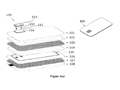
Referring to Figure 1(a), an exploded view of a dual interface smart card with
metal face layer is depicted. The dual interface smart card (100) comprising
of, a
metal layer (101), a self-adhesive layer (102), a magnetic layer, a dual
adhesive
layer (104), an antenna (105), an antenna inlay layer (106), a printed layer,
an
CA 03224843 2024- 1-3
WO 2023/131825
PCT/1B2022/056762
12
overlay layer with magnetic strip, a filler material (110), a solder paste
(111), a
heat activated glue tape (112), integrated circuit chip module (113).
Referring to Figure 1(b), a side view of the dual interface smart card with
metal
face layer is depicted. The dual interface smart card (100) has thickness
ranging
from SOO to 810 micron with integrated circuit chip module that is embedded on
the metal layer (101).
Referring to Figure 2, a flow chart of manufacturing method of dual interface
smart card with metal face layer is depicted. The method for manufacturing a
dual
interface smart card (100) with metal face layer, comprises the steps of, a)
preparing a metal layer (101), b) selecting a dual adhesive layer (104) and a
magnetic layer, c) preparing an antenna layer, d) preparing a plastic back
layer, e)
preparing a magnetic layer and an adhesive layer, f) collating said layer and
layer
to form an assembly of said dual interface smart card (100), g) laminating
said
assembly and preparing an integrated circuit chip module for implanting, and
h)
milling said metal card to implant said integrated circuit chip module which
produces said dual interface smart card (100) with metal face layer, wherein,
said
metal layer (101) is processed for creating a pin hole through an automated
tool,
said dual adhesive layer (104) and magnetic layer are collated together and a
hole
is created on said collated dual adhesive layer (104) and magnetic layer, said
antenna layer is prepared by embedding an antenna (105) on a plastic layer and
said antenna layer is flattened by a lamination process which forms an antenna
inlay layer (106), said plastic back layer is printed with any information and
plurality of magnetic strips are transferred on an overlay layer (108), said
antenna
inlay layer (106), plastic back layer and said overlay layer (108) are spot
welded
together and laminated to create a laminated back layer for avoiding shrinkage
and expansion of said layers and a pin hole is created on said laminated back
layer, said metal layer (101), dual adhesive layer (104), said laminated back
layer
are collated and a filler material (110) is applied through said hole created
in said
metal layer (101) to form said assembly, said assembly is laminated to form a
laminated metal card, said milling of said metal card to implant said
integrated
CA 03224843 2024- 1-3
WO 2023/131825
PCT/1B2022/056762
13
circuit chip module is done through a Te-connect process that helps to obtain
higher throughput as compared to thermal soldering process.
Referring to Figure 3(a) and Figure 3(b), a perspective and side views of a
hole in
the metal layer of the present invention is depicted. The metal layer (101) is
selected in sheet format which is heat treated to improve strength and tension
and
intended to serve as the top layer of a card which is 300 series grade
(specifically
304/ 316) stainless steel combined with other alloys with thickness ranging
from
380 to 400 microns. The metal layer (101) is then processed to form a through
hole
in known manner including, but no limited to: milling, laser cutting etc. The
dimension of the through hole is set higher than the dimension of the
integrated
circuit chip module used to form the card. The advantage of making larger
through hole then dimension of integrated circuit chip module is to provide
greater
separation between the metal layer (101) and the integrated circuit chip
module
and thus enhance transmission. The through hole may be of square, a rectangle
or
a circle in shape based on the integrated circuit chip module selected.
The metal layer (101) has width (SH) in range from 450 to 485 mm and height
(SW) in range from 250 to 300 mm. The thickness (D1) of the sheet is in range
from 390 to 400 micron as shown in Figure 3(b). This metal layer (101) is
first
milled to obtain two pin hole of size in range from 2 to 3 mm in diameter
which
are located 68 to 71.56 mm away from the top of layer and bottom edge. These
pins help to hold the material firm during milling process. The metal layer
(101) is
then placed on the CNC_ (Computer Numerical Control) milling machine to create
through hole (201) on metal layer (101) with width (W1) and length (L1) being
at
least 0.8 mm higher than the integrated circuit chip module dimensions. As
illustrated in Figure 3(a) about 20 to 24 through holes (201) are created in
the
metal layer (101) with vertical distance between these through holes (TH) is
in
range from 50 to 56.98 and horizontal distance (TW) is in range from 85 to 91
mm.
Referring to Figure 4(a) and Figure 4(b), top and side views of the antenna in
the
present invention is depicted. The antenna (105) is embedded into the antenna
CA 03224843 2024- 1-3
WO 2023/131825
PCT/1B2022/056762
14
inlay layer (106) by using copper wire antenna embedding machine. The antenna
inlay layer material is held using vacuum and magnetic guide on wire embedding
machine so to ensure the antenna sheet stays firm using antenna embedding
process. The antenna (105) is designed to resonate at 13.56 mhz. the antenna
designs are recommended by integrated circuit chip module as depicted in
Figure
4(a).
The antenna inlay layer (106) is processed for antenna flattening process by
applying heat, cold and pressure using standard lamination machine. Lamination
process is carried out by applying a pressure in range from 700 to 800 psi in
multiple steps at hot temperature of 152 C for about 10 to 12 minutes and by
then
cooling the sheets at 20 to 25 C and by applying pressure of 1200 to 1500 psi
for
12 to 14 minutes again at multiple steps to form laminated antenna inlay layer
(106) having thickness (AT) of 150 microns as depicted in Figure 4(b).
Referring to Figure 5(a), a top view of antennal inlay layer is depicted. The
antenna inlay layer (106) along with printed layer (107) and overlay with
magnetic
stripe (108) are collated, spot welded to ensure all plastic materials are
held intact.
The spot welded sheets are then created with pin hole of 2 to 3 mm diameter
and
processed for lamination using standard lamination process to form a first
assembly. The position of the pin hole is matched with the pin hole created in
the
metal layer (101).
Referring to Figure 5(b), another top view of antennal inlay layer after being
welded and laminated. The first step lamination process is carried out by
applying
a pressure ranging from 700 to SOO psi at hot temperature that lies in range
from
150 to 152 C for about 12 to 16 minutes and by then cooling the layer at
temperature ranging from 20 to 25 C and by applying pressure of 1200 to 1500
psi
for 12 to 16 minutes. The side view of the card after first lamination is
depicted in
Figure 5(c).
Referring to Figurc 6(a), a top view of through hole punched in the area for
adhesive layer in the present invention is depicted. The Error! Reference
source
CA 03224843 2024- 1-3
WO 2023/131825
PCT/1B2022/056762
not found. layer (104) is used to bond metal layer (101) with magnetic layer
(103)
and with antenna inlay layer (106). The magnetic layer (103) serves to shield/
prevent/reduce metal layer (101) from interfering with an electromagnetic
field
that occur when the antenna (105) operates through communication with an
5
external antenna reader. The magnetic field generated from antenna (105)
interacts with the metal layer (101), and self-resonant frequency of the
antenna is
changed so that the inductance of the antenna (105) is lowered to cause
communication troubles, which is because of eddy current generated from metal
layer (101) by mean of magnetic field. To eliminate this, the magnetic layer
(103)
10 haying
high permeability and high resistance is located between metal layer (101)
and inlay layer to adjust the magnetic field lines.
Referring to Figure 6(b), a side view of the magnetic sheet that is sandwiched
with
the adhesive layer is depicted. The magnetic layer (103) is sandwiched with
adhesive layer in the form of film (102 and 104) are all collated to form one
layer
15 (AL).
the size of this layer is same as that of the metal sheet layer. This layer is
then punched using sheet punching machine to create a through hole to match
with the metal layer (101) through hole.
Referring to Figure 7(a), a top view of a laminated back layer in dual
interface
smart card is depicted. The laminated back layer used herein comprise of the
antenna (105), antenna inlay layer (106), printed layer (107) and overlay
layer
(108) with magnetic stripe that collated together. Referring to Figure 7(b),
another
top view of the laminated back layer with placement of magnetic and adhesive
layers is depicted. The adhesive layer with magnetic layer (103) is collated
and
placed on the laminated back layer.
Referring to Figure 7(c), top view of the adhesive layer is depicted over
which the
metal layer is placed. The metal layer (101) having through hole is placed on
the
adhesive layer and collated. Referring to Figure 7(d), a perspective view of
the
collated metal layer (101), adhesive layer and laminated back layer is
depicted.
The metal layer (101), magnetic layer (103) sandwiched with adhesive layer
(AL)
and back layer (UT) are collated and spot-welded using spot welding table.
CA 03224843 2024- 1-3
WO 2023/131825
PCT/1B2022/056762
16
Referring to Figure 7(e) is a diagrammatic view of spot welding all layers and
Figure 7(f), is an exploded view of all the layers. The table includes heating
rod
and numatics cylinder helps to apply pressure and heat on a specific spot
which
melts and holds all layers temporally to form one single sheet having
thickness of
820 microns and processed for next process.
Referring to Figure 8(a), a diagrammatic view of placement of filler material
on
the metal layer through the hole is depicted. The collated and spot-welded
assembly containing the metal layer (101) with through hole, is then inserted
with
Error! Reference source not found.like is used which does not interfere with
transmission. The Error! Reference source not found.(110) is placed ensuring
that
the interior walls of the through hole (201) and or the exterior walls of the
Error!
Reference source not fotuid.(110) adheres firmly to the walls of the through
hole
(201). Referring to Figure 8(b), another exploded view of filler layers in the
dual
interface smart card (100). The filler material (110) is inserted with
thickness (F1),
20 microns lesser than the metal layer (101). The width and height of the
filler
material (110) is same as that of through hole (201) dimensions on metal layer
(101) and processed for second lamination process. The filler material (110)
bonds
with a back layer without using any adhesive underneath said filler material
(110).
Referring to Figure 9(a), an isometric view of a lamination plate with
embossed
layer is depicted. The second step lamination process is carried out using
lamination plate having embossed / raised layer on plate to ensure pressure is
evenly applied on filler material (110) during lamination process. The
thickness of
the embossed layer is preferably not greater than 20 microns. Referring to
Figure
9(b), a perspective view of lamination plate with metal top surface and
plastic back
surface. Second step lamination process is carried out by applying a pressure
of
500 to 700 psi at hot temperature of 175 C for about 18 minutes and then
cooling
the layers at 25 C by applying pressure of 900 to 1000 psi for 18 minutes. The
total
thickness of after lamination (CT) is approx. is 800 to 810 microns. The
exploded
view of all layers in the card is depicted in Figure 9(c).
CA 03224843 2024- 1-3
WO 2023/131825
PCTI1B2022/056762
17
Referring to Figure 10(a), is a top view of the laminated plate that is CNC
milled
to form the card. The laminated plate having thickness of 800-810 micron is
then
processed through CNC milling to create individual card (CU) which contains
through hole on metal surface (101) layer. The vertical distance (CH) 55.48 mm
between the card and horizontal distance (CW) between the card is 91mm. having
plate size of (SH) 485 mm and (SW) 300 mm. Referring to Figure 10(b), a front
view of the dual interface card after CNC milled step is depicted. The
dimension
of the individual card is as illustrated in the Figure 10(b) with Width (W) of
the
card being 85.6 mm and height(H) of the card being 53.98 mm in size. The
position of the through hole is located from top edge of the card (MH) 18.5 mm
and (MW) is 9.5 mm from side edge of the card.
Referring to Figure 11, a flow chart of method for milling an integrated
circuit
chip module and implanting a cavity in a dual interface smart card is
depicted.
The method for milling an integrated circuit chip module (113) and implanting
a
cavity in a dual interface smart card (100), comprises steps of a) milling a
card
with filler layer for accommodating surface of the integrated circuit chip
module
(113) till plurality of antenna (105) terminals are exposed, b) selecting the
integrated circuit chip module (113) and applying a heat activated glue tape
(112)
on the integrated circuit chip module (113) for exposing plurality of
connectors of
the integrated circuit chip module (113), c) placing the integrated circuit
chip
module (113) that is obtained from step(b) on a milled product obtained
through
step (a); and d) applying a solder past on the antenna (105) terminals for
embedding the integrated circuit chip module on the card.
Referring to Figure 12(a), a front and top view of integrated circuit chip
module is
depicted. The integrated circuit chip module (113) having dual interface
connector
(115 and 116) option on rear side of the integrated circuit chip module to
connect
to antenna layer (105) to enable dual interface function is selected. The
integrated
circuit chip module modules used herein are in different shapes, sizes, PIN
configuration. However, the preferable dimensions of the integrated circuit
chip
module (IW) is 11 mm and height (IH) is 8.5 mm.
CA 03224843 2024- 1-3
WO 2023/131825
PCT/1B2022/056762
18
Referring to Figure 12(b), a diagrammatic view of the heat activated glue tap
that
is applied on the integrated circuit chip module is depicted. The integrated
circuit
chip module (113) is processed through glue tape lamination machine where heat
activated tape (112) is die cut and transferred onto the rear side of the
integrated
circuit chip module. The shape of glue tape (112) is formed as per integrated
circuit chip module dimension. The glue tape (112) is die cut to a shape to
ensure
that the glue tape is not transferred on to the connectors (115 and 116) and
left
open with approximate dimension of height (GIH) 6.6 mm and width (GIW) 8.2
mm. The dimension of the applied glue tape having width (GW) 11 mm and
height (GH) 8.5 mm is as per the integrated circuit chip module (113) size
selected.
Referring to Figure 12(c), a schematic view of the integrated circuit chip
module is
depicted. The overall thickness (I3) of the integrated circuit chip module
(113) is
approx. 580 micron and thickness of integrated circuit chip module tape is (H)
is
approximately 220 microns and the thickness (I2) of glue tape (112) is approx.
45
50 micron. The bottom width of integrated circuit chip module (I4) is smaller
than
the width of (GIW).
Referring to Figure 13(a), a side view of the first and second cavity milling
in the
dual interface card is depicted. The integrated circuit chip module (113)
milling
and implanting process is carried out using automated milling and embedding
machine using the technology named Te-Connect. In this process card body is
milled to accommodate integrated circuit chip module (113) shape, size and
connector pads are connected to antenna terminals using solder paste. The
transferred glue tape on rear side of the integrated circuit chip module (113)
and
dispensed solder paste on (C3) milled cavity are activated by applying heat
and
pressure followed by cooling and pressure on integrated circuit chip module.
The
metal card containing filler material (110) is processed for milling to
accommodate
integrated circuit chip module on the body of the dual interface card. The
cavity is
formed through the filler material (110) to a depth (Cl) 240-260 microns from
the
top surface to accommodate integrated circuit chip module and glue tape al and
CA 03224843 2024- 1-3
WO 2023/131825
PCT/1B2022/056762
19
12) thickness. Since the width of (Cl) is lesser than the through hole (201),
This
helps to create insulation layer (IL) between metal edge surface and
integrated
circuit chip module edges. The second cavity (C2) is milled at least 20
microns
higher than integrated circuit chip module thickness (I3) and width of cavity
(C2)
is created at least 1 mm higher than the bottom width of integrated circuit
chip
module (14).
Referring to Figure 13(b), a side view of the third and fourth cavity milling
in the
dual interface card is depicted. The body of the dual interface card is then
milled
(C3) to the depth till antenna terminals are exposed approx. 580-590 micron.
The
(C3) is milled in circular shape (C3D) having diameter of 1.5 mm.
Referring to Figure 13(c), a diagrammatic view of milling shape and dimensions
on filler material (110) as per integrated circuit chip module (113). The
milled C3
is filled with solder paste (111) which is conductive in nature and is heat
treated to
solidify and bond. The solder paste (111) is applied just before implanting
the
integrated circuit chip module (113), which helps to connect antenna (105)
terminals with integrated circuit chip module connectors (115 and 116).
Referring to Figure 13(d), a side view of the dual interface card depicting
the
dispensing of solder paste (111) into the cavity. The integrated circuit chip
module
(113) is implanted into the milled section of card body and ascertained that
the
integrated circuit chip module is leveled to the top surface of the card body.
Referring to Figure 13(e), another side view of the dual interface card is
depicted
that shows the embedding of the integrated circuit chip module into the
surface of
the card. The implanting process is carried out with adequate pressure and
heat on
top surface of integrated circuit chip module. The glue tape (112) on
integrated
circuit chip module and solder paste (111) filled on (C3) is activated by heat
and
pressure. The integrated circuit chip module is then gradually cooled down
with
lower temperature and pressure. Referring to Figure 13(e), a diagrammatic view
of
embedding of integrated circuit chip module on the card surface is depicted.
The
integrated circuit chip module is ensured that it is 10 microns above the card
surface so to enable top surface of the integrated circuit chip module comes
in
CA 03224843 2024- 1-3
WO 2023/131825
PCT/1B2022/056762
contact with contact reader (Ex: POS, ATM). The integrated circuit chip module
also enables contactless reading (on POS, ATM) as it is now enabled with the
same.
Referring to Figure 14, a perspective view of the dual interface smart card is
5 depicted, in which the two-step lamination process helps to avoid
shrinkage and
expansion of layers when laminating with other type of substrates. The first
lamination is processed by laminating all plastic layers such as antenna inlay
layer
(106), printed sheet and overlay layer (108) with magnetic stripe and in
second
lamination process. The metal layer (101) with adhesive and magnetic sheet
along
10 with filler material is laminated together to form single assembly.
Furthermore, the
lamination plate having embossing/raise effect on through hole area helps to
maintain even pressure during lamination process. The filler material strongly
bonds with back layer without using any adhesive underneath the filler
material.
The through hole is created on metal surface and filler material is placed
which
15 provides support and creates insulation between integrated circuit chip
module is
and metal layer (101), cavity is created on filler material to implant the
integrated
circuit chip module is using le-Connect enabled machine. the Te-Connect
Process helps in obtaining higher throughput compared to thermal soldering
process. The major advantage of the present invention is the reducing number
of
20 steps in process of manufacturing metal surface cards.
EXAMPLE 1
EXPERIMENTAL DATA ANALYSIS
The present invention provides a dual interface smart card, which contributes
significantly towards achieving higher output and a smart card, which reduces
process during production by avoiding using any adhesive below filler
material.
The throughput details of the chip embedding machine followed in conventional
and present invention are depicted in Table 1_
Table 1
CA 03224843 2024- 1-3
WO 2023/131825
PCT/1B2022/056762
21
Throughput details of the chip embedding machines
Process Speed
(CPH: cards per hour)
Soldering Process followed in
1,500 CPH
conventional methods
Te-Connect followed in
2200, CPH
present invention
The magnetic layer prevents the metal layer from interfering with an
electromagnetic field that is generated from the antenna and the magnetic
layer
has high permeability with high resistance and placed between the metal layer
and
the antenna inlay layer for adjusting plurality of magnetic field lines of the
electromagnetic field. Table 2 and Figure 15 presents data related to high
permeability with high resistance of metal in the dual interface smart card.
Table 2
Data related to high permeability with high resistance of metal in the dual
interface smart card
Relativ
Mate Relative Saturate
Surfac Therma e
Operati
rial Permeabili d Curie
1
Permitt ng
Name ty magnetic
ivity
[at
Rcsisti Conduc Flux Temper
temper
13.56MHz
vity tivity density
ature ature
(Ohm (at
u u u'/ (W/m
/sq.)
(mT) ( C) 1MHz) ( C)
11" = K)
tYP. tYP.
Mater
ial
used
100
in 4 O.
¨40 to
50 10M 1.5 [H=1194 > 500 1450
prese 0 8
+85
A/m]
nt
invent
ion
CA 03224843 2024- 1-3
WO 2023/131825
PCT/1B2022/056762
22
For calculating the resistance for the area of metal in the dual interface
smart card,
the equation (1) is used, wherein "R" refers to resistance.
R = p*L/W (1),
L/w=86/54-1.59 (Approx.), p=10MQ,
Hence, R=15.9MQ
Therefore, the present invention provides a metal smart card, which
contributes
significantly towards achieving higher output and a metal smart card, which
reduces process during production by avoiding using any adhesive below filler
material.
Many modifications and other embodiments of the invention set forth herein
will
readily occur to one skilled in the art to which the invention pertain having
the
benefit of the teachings presented in the foregoing descriptions and the
associated
drawings. Therefore, it is to be understood that the invention is not to be
limited to
the specific embodiments disclosed and that modifications and other
embodiments
are intended to be included within the scope of the appended claims. Although
specific terms are employed herein, they are used in a generic and descriptive
sense only and not for purposes of limitation.
CA 03224843 2024- 1-3