Note: Descriptions are shown in the official language in which they were submitted.
Abstract
The present invention relates to a method by means of which defects in
materials, preferably in solid
bodies (18), can be localized with considerably higher spatial resolution than
before. With the
present invention, such defects can be quickly and economically imaged with
high spatial resolution.
Above all, with the present invention it is possible to contactlessly spin-
selectively excite and capture
or image defects in the solid body with high sensitivity, high dynamic range,
large field of view and
excellent resolution, which far exceeds the present capabilities of optical
detection processes.
Furthermore, with the process according to the invention there is an excellent
possibility for
detecting spin even in individual images, wherein high contrast of the spin
states and better fidelity
of reproduction of the spin states are made possible. The device (10)
according to the invention and
the process according to the invention are also extremely useful for quantum
calculation using defect
spins in solid bodies (18), for quantum-capable capturing and for quantum-
capable measurement
networks.
CA 03224966 2024- 1-4
Process and device for the spatially resolved localization of defects in
materials
The present invention relates to a process for the spatially resolved
localization of defects in
materials according to the general concept of claim 1 and a device for the
spatially resolved
localization of defects in materials according to the general concept of claim
14.
Within the framework of the present invention, a defect in a material is
understood to be a structural
or chemical change with which one or more electrons are captured and localized
at the site of the
defect. Such defects are mainly known from solid bodies. However, they could
also be liquids or
gases. The material can also contain one or more molecules.
If the material is insulating or semiconducting or has a band gap, such
defects are characterized by
electrons that have an energy level that lies within the band gap of the host
material in the ground
state (see Bassett, L. C., etal. (2019) "Quantum defects by design,"
Nanophotonics, 8(11), pp. 1867-
1888, DOI: 10.1515/nanoph-2019-0211). Such electrons can be excited to higher
states and then
return to the ground state through radiative or non-radiative processes.
Defects that absorb photons
and subsequently emit luminescence photons are called color centers. There are
countless color
centers in the solid state. For example, more than 500 types of luminescent
color centers are known
for diamond (see Zaitsev, A. M. (2001) Optical Properties of Diamond. Berlin,
Heidelberg: Springer
Berlin Heidelberg, DOI: 10.1007/978-3-662-04548-0). However, other materials
such as silicon
carbide (see Castelletto, S. et al. (2014), "A silicon carbide room-
temperature single-photon source,"
Nature Materials, 13(2), pp. 151-156, DOI: 10.1038/nmat3806), quartz and even
two-dimensional
materials, such as hexagonal boron nitride (see Tran, T. T. et al. (2016)
"Quantum emission from
hexagonal boron nitride monolayers," Nature Nanotechnology, 11(1), pp. 37-41,
DOI:
10.1038/nnano.2015.242), can also exhibit luminescence defects.
As mentioned, the electrons associated with these defects can absorb a
specific wavelength band
and emit a corresponding long-wavelength photon with a characteristic lifetime
in the excited state.
The emitted long-wavelength photons are usually collected through a microscope
objective lens with
a high numerical aperture (NA) and captured by a single photon counter or a
photomultiplier tube.
The device that can carry out this imaging is a confocal optical microscope.
However, such optical
detection has a resolution limitation, which is defined by half the wavelength
of the light used for
detection:
Optical resolution d = (0.51=A}/NA
CA 03224966 2024- 1-4
Such resolution limit poses a major problem if a plurality of closely spaced
color centers (defects in
solid-body materials) are to be imaged. Although there are some methods to
surpass this diffraction-
limited resolution, such as STED ("stimulated emission depletion" - see Hell,
S. W. and Wichmann, J.
(1994) "Breaking the diffraction resolution limit by stimulated emission:
stimulated-emission-
depletion fluorescence microscopy," Optics Letters, 19(11), p. 780, DOI:
10.1364/0L.19.000780) (see
Rittweger, E. et al. (2009) "STED microscopy reveals crystal color centres
with nanometric
resolution," Nature Photonics, 3(3), pp. 144-147, DOI:
10.1038/nphoton.2009.2), microwave-assisted
STORM ("stochastic optical reconstruction microscopy" - see Pfender, M. etal.
(2014) "Single-spin
stochastic optical reconstruction microscopy," Proceedings of the National
Academy of Sciences,
111(41), pp. 14669-14674, DOI: 10.1073/pnas.1404907111) and gradient-encoded
imaging (see Arai,
K. et al. (2015) "Fourier magnetic imaging with nanoscale resolution and
compressed sensing speed-
up using electronic spins in diamond," Nature Nanotechnology, 10(10), pp. 859-
864, DOI:
10.1038/nnano.2015.171) (see Zhang, H. et al. (2017) "Selective addressing of
solid-state spins at the
nanoscale via magnetic resonance frequency encoding," npj Quantum Information,
3(1), p. 31, DOI:
10.1038/s41534-017-0033-3) etc. However, these are comparatively slow and
require pixel-by-pixel
scanning, which prevents any possibility of observing a large number of
defects.
It is therefore the object of the present invention to provide a method with
which defects in
materials, preferably in solid bodies, can be localized with higher local
resolution. In particular, such
defects are to be imaged with high local resolution, which is particularly
quick and cost-effective.
This object is achieved by the process according to the invention according to
claim 1 and the device
according to the invention according to claim 14. Advantageous further
developments are indicated
in the dependent claims and in the following description together with the
figures.
It was recognized by the inventors that this object can be achieved in a
surprisingly simple way by
exciting the electrons associated with the defects with such energy that they
are emitted from the
material, and subsequently performing an electron imaging in order to
determine the spatial position
of the electrons emerging from the surface of the solid body and thus the
corresponding defects.
The process according to the invention for the spatially resolved localization
of a defect in a material,
wherein the material has a band gap, wherein the defect has one or more
electrons having at least
CA 03224966 2024- 1-4
- 2 -
one energy level that lies in the band gap, characterized in that the electron
is excited such that it is
emitted from the material and subsequently an electron imaging is carried out.
Although the process of photoemission electron microscopy (PEEM), with which
an imaging of
emitted electrons is also effected, has also been used, this process does not
achieve the necessary
spatial resolution to detect defects in materials (i.e., a structural or
chemical change with which an
electron or a plurality of electrons are captured and localized at the
location of the defect) in a
spatially resolved manner. Instead, PEEM has only ever been used to
characterize the bulk material
(such as mass, lattice and ensemble of the material). Therefore, PEEM can be
used to examine defect
ensembles at most, wherein, for example, according to the publication K.
Fukumoto etal.: "Imaging
the defect distribution in 2D hexagonal boron nitride by tracing
photogenerated electron dynamics,"
J. Phys. D: Appl. Phys. 53 (2020) 405106 (9pp), DOI: 10.1088/1361-6463/ab9860,
a maximum
resolution of 100 nm can be achieved, which is too low for the spatially
resolved localization of a
single defect or even quantum applications. By contrast, with the use of
transmission electron
microscopy (TEM), in particular cryo-TEM, spatial resolutions of up to 0.1 nm
can be achieved.
In an advantageous further development, it is provided that at least one of
the following elements is
used: Aberration correction element, means for high magnification, objective
lens with high
numerical aperture, focusing element and acceleration column for increasing
the energy of the
electrons, because this allows very high resolutions to be achieved with high
image quality and image
robustness and automatic alignment.
In an advantageous further development, it is provided that the defect is
imaged with a spatial
resolution of at least 25 nm, preferably at least 20 nm and in particular in
the range of 0.1 nm to 20
nm. This makes quantum applications possible, because quantum mechanical
interactions of spins
can then be resolved, which occur if such spins are spaced apart in the range
of up to 25 nm.
In an advantageous further development, it is provided that electron imaging
is carried out with the
aid of electron optics and an electron detector, because the corresponding
setup for the optics and
detection, i.e. except for the electron source, can then be used by a
conventional - for example, a
commercially available - electron microscope, in particular a transmission
electron microscope.
Preferably, a microchannel plate (MCP - a two-dimensional, image-resolving
secondary electron
multiplier), a direct electron detector, an electron multiplier CCD (EMCCD),
an sCMOS (scientific
CMOS) or a phosphor screen is used as the electron optics (26, 28, 30, 32),
which enables images
CA 03224966 2024- 1-4
- 3 -
with high spatial resolution to be taken. Preferably, a magnetic element or an
electromagnetic
element is used as the electron optics, because this makes it particularly
easy to collect and direct
the electrons / manipulate the electrons for magnified imaging.
In an advantageous further development, it is provided that the excitation of
the electron is effected
by one or more electromagnetic waves, preferably light (infrared (300 GHz to
384 THz), visible light
(384 THz to 789 THz), ultraviolet light (789 THz to 30 PHz)), radio waves
(ultrashort waves (30 MHz to
300 MHz), short waves (3 MHz to 30 MHz), medium waves (300 kHz to 3 MHz) and
long waves (30
kHz to 300 kHz)), terahertz radiation (0.1 THz to 10 THz), low frequency (1
kHz to 30 kHz) or
microwaves (1 GHz to 300 GHz). This makes it particularly easy to emit the
electrons and the
excitation energy can be defined for subsequent evaluation.
In an advantageous further development, it is provided that the excitation is
focused on a region,
preferably a surface region of the material, wherein in particular light is
used that is focused by one
or more optical elements, preferably an objective lens with a high numerical
aperture, or that the
excitation is effected with a LASER light source or that the excitation is
effected in evanescent wave
geometry or that the defect is arranged in a light-confining nanostructure,
cavity or optical resonator.
With excitation in evanescent wave geometry, the excitation can be limited to
a depth of a few
nanometers below the surface. By using a light-confining structure, such as a
cavity, the excitation
can be directed only to a specific defect. One or more of these measures can
further increase the
local resolution by stimulating only specific defects from the outset. It is
also possible to select
specific defects. Overall, one or more of these measures can be used to shape
the excitation and
thereby enable photoexcitation of the defect and subsequent photoemission of
electrons from
ranges much smaller than the diffraction limit (1 nm - 1300 nm), as a result
of which even higher
localization resolutions, sensitivities and dynamic ranges are achieved.
In an advantageous further development, it is provided that the spin state of
the electron is
determined by one or more additional excitations, wherein the additional
excitation is effected by
electromagnetic waves, preferably light (infrared (300 GHz to 384 THz),
visible light (384 THz to 789
THz), ultraviolet light (789 THz to 30 PHz)), radio waves (ultrashort waves
(30 MHz to 300 MHz), short
waves (3 MHz to 30 MHz), medium waves (300 kHz to 3 MHz) and long waves (30
kHz to 300 kHz)),
terahertz radiation (0.1 THz to 10 THz), low frequency (1 kHz to 30 kHz) or
microwaves (1 GHz to 300
GHz), by electromagnetic fields, by thermal processes or by thermionic
processes. This allows, for
example, interactions between different defects to be examined / the status of
a defect to be read
CA 03224966 2024- 1-4
- 4 -
out, as a result of which qubit applications in particular are enabled. By
using the determination of
spin states and the spin state-selective excitation of electrons from the
material and subsequent
imaging, the defects are resolved spatially and simultaneously by their spin
states.
In an advantageous further development, it is provided that the material is
electrically grounded.
This prevents the examination from being influenced by a charge on the
material.
In an advantageous further development, it is provided that a bias voltage is
applied across the
surface of the material, wherein the bias voltage is preferably positive. This
facilitates and improves
the extraction of the emitted electrons and their transfer to the electron
image. If the bias voltage is
applied to an electrode, preferably a lattice, a large number of electrons can
be accelerated
simultaneously, such that a plurality of electrons can be examined in
parallel, i.e. large-area imaging
is possible. Alternatively, if the bias voltage is applied to a tip, the local
resolution can be improved
even further. However, a plurality of tips would then be required for parallel
observation of a
plurality of electrons. Serial scanning of the surface of the solid body could
then be carried out using
one or more tips.
In an advantageous further development it is provided that the material is
doped, preferably doped
with a donor. For example, it can be boron. This provides a defect with
electrons in a particularly
reliable manner, such that the defects can be examined more easily. However,
the process according
to the invention also works in principle without doping.
In an advantageous further development, it is provided that the defect is
created by at least one of
the methods from the group comprising: Implantation after production of the
material, doping
during production of the material and by electron irradiation during or after
production of the
material. This allows defects to be created particularly easily and
nevertheless in a determined
manner, in particular with regard to their localization.
In an advantageous further development, it is provided that the surface of the
material has been
provided with a thin conductive layer, wherein the layer is preferably a
metallic layer or a metal-
coordinated molecular layer, wherein the layer consists in particular of one
or two to five
monolayers. This facilitates the emission of the excited electrons. The layer
can preferably be applied
as a "coating," i.e. by means of a coating process. However, the process
according to the invention
also works in principle without such a layer.
CA 03224966 2024- 1-4
- 5 -
In an advantageous further development, it is provided that the material is
surrounded by a magnetic
shield. This can be a soft magnetic material, for example. This increases
precision, because external
magnetic fields, such as the earth's magnetic field, cannot influence the
electron emission or the
path of the emitted electron.
In an advantageous further development, it is provided that the material is
surrounded by a Faraday
cage. This also increases the precision because external electromagnetic
fields, such as those from
electrical power lines, cannot influence the electron emission or the path of
the emitted electron.
In an advantageous further development, it is provided that the material is
arranged in a vacuum
with a pressure of a maximum of i0 mbar, as a result of which the defects can
be localized with
particularly good spatial accuracy, because the electrons emerging from the
surface of the material
are not disturbed by particles.
In an advantageous further development, it is provided that the material is
cooled, wherein the
cooling is preferably effected in the temperature range of 0.1 K to 210 K.
As a result, the defects
have a defined excitation spectrum that is selective for the spin state.
In an advantageous further development, it is provided that the material is
present as a solid body,
preferably as a layer or bulk material, and in particular comprises a
substance from the group:
Diamond, silicon, silicon carbide, hexagonal boron nitride and crystalline
materials with a band gap in
the range of 0.1 eV to 14 eV. Extensive information is available on the
defects of such solid bodies.
The layer can preferably be present as an atomically thin layer in the sub-
nanometer range or as a
crystalline two-dimensional layer.
Independent protection is claimed for the device according to the invention
for the spatially resolved
localization of a defect in a solid body, wherein the solid body has a band
gap, wherein the defect has
one or more electrons that has at least one energy level that lies in the band
gap, characterized in
that there are means for exciting the electron that are adjusted to excite the
electron, such that it is
emitted from the solid material, and there are means for electron imaging.
In an advantageous further development, it is provided that the device is
adjusted to carry out the
process according to the invention.
CA 03224966 2024- 1-4
- 6 -
In an advantageous further development, it is provided that the device has the
structure of a
transmission electron microscope, wherein the material is arranged instead of
an electron filament
of the transmission electron microscope. The device is then particularly easy
to produce and has a
very high spatial resolution with high image quality and image robustness and
automatic alignment.
In an advantageous further development, it is provided that the device is a
component of a quantum
computer or a quantum sensor. This means that quantum computers and quantum
sensors can be
operated with greater precision.
Independent protection is claimed for the use of the process according to the
invention or the device
according to the invention, which is characterized by the fact that quantum
computing applications,
quantum-based information processing or quantum sensing applications are
carried out with it. Such
processes can now be carried out with even greater precision. A very high
spatial resolution can then
be achieved, particularly in the field of quantum sensor technology.
In an advantageous further development, it is provided that the corresponding
parts of an electron
microscope are used as means for electron imaging. The entire device can thus
be formed by an
electron microscope that has an electron excitation, preferably a light
excitation, in particular a
LASER excitation, instead of or in place of the electron source.
The features and further advantages of the present invention will become
apparent below from the
description of two preferred exemplary embodiments in connection with the
figures. Thereby, the
following are shown, purely schematically:
Fig. 1 the process according to the invention according to a first
preferred embodiment and
Fig. 2 the process according to the invention according to a
second preferred embodiment.
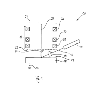
Fig. 1 shows the device according to the invention in accordance with a first
preferred embodiment.
It can be seen that the device 10 according to the invention has means 12 for
electron excitation and
means 14 for electron imaging.
CA 03224966 2024- 1-4
- 7 -
The electron excitation means 12 have, for example, a suitably controlled
LASER source 12, whose
LASER beam 16 can be directed onto a sample 18 arranged in a suitable holder
(not shown), wherein
one or more optical elements 19, such as high refraction objective lenses,
lenses and optical beam
sharpeners, can be used to define the beam. The electron excitation means 12
can be movable in
their orientation with respect to the sample 18, such that the LASER beam 16
can be directed to a
specific point 20 on the surface 22 of the sample 18. Thereby, the sample is
grounded such that it
cannot become charged.
In the example shown, the optical source 12 illuminates the sample 18 from
above. This is
particularly useful for samples that are not radiolucent. If, on the other
hand, the sample 18 is
opaque, the irradiation 16 can in principle also occur from any side of the
sample 18, i.e. also through
a side surface of the sample 18 or from below through the sample 18.
The electron 24 associated with a defect in the sample 18 is emitted by the
excitation 16, if this has a
sufficiently high energy, and is subsequent accelerated 27 by a metallic
lattice 26 arranged above the
surface 22 of the sample 18, to which a positive bias voltage is applied, such
that it can be taken over
by the electron image 14, or more precisely by a condenser lens 28. The bias
voltage must be
selected as a function of the geometry of the electrode and can range from a
few mV to a plurality of
kV, for example.
The accelerated electron 27 subsequently passes through an objective lens 30
and a projective lens
32 to ultimately hit a CCD surface 34. The resulting image (not shown)
represents, depending on the
selected optical parameters, a complete image of image in sections of the
spatial coordinates of the
surface 22 and shows the locations at which the electrons 24 were emitted,
indicating directly the
position of the defects in relation to the surface 22 of the sample 18.
The elements of the electron optics, i.e. condenser lens 28, objective lens 30
and projective lens 32,
along with the electron detector 34 are standard components of a transmission
electron microscope
and are known to the person skilled in the art, which is why they are not
explained in more detail
here. Thus, conventional TEMs can preferably be used within the framework of
the present
invention, wherein, however, the electron filament is removed and the sample
18 is placed there
instead. The actual sample holder of the TEM remains empty instead. Thereby,
all other elements of
the TEM can still be used, although the first of two standard capacitors of a
TEM, for example, would
not be required, but can still be used. This allows very high resolutions to
be achieved with high
CA 03224966 2024- 1-4
- 8 -
image quality and image robustness and automatic alignment, because such TEM
has aberration
correction elements, high magnification, objective lenses with high numerical
aperture, focusing
elements and acceleration columns to increase the energy of the electrons.
The person skilled in the art is also familiar with the fact that there should
be a vacuum between the
sample surface 22 and the electron detector 34, so that the electrons 24, 27
are not undesirably
influenced.
A commercial electron microscope, in particular a commercial transmission
electron microscope, can
thus be used for the realization of the device according to the invention,
wherein its electron source
and the electron accelerator can be dispensed with, but need not be. In any
case, the means 12 for
electron excitation in the sample 18 must be used and, to improve the device,
the means 26 for
generating a bias voltage must also be used.
The process according to the invention using the device 10 according to the
invention is to be
explained in more detail below with reference to the localization of defects
in the form of nitrogen
defect centers in diamond. However, the same process can also be used for any
other defects and
materials.
Nitrogen-vacancy (NV) centers in diamond are defects in the carbon lattice
that occur when a single
carbon atom is substituted by a nitrogen atom and at the same time a gap is
created in adjacent
lattice sites. In the negative charge state, the NV center has two unpaired
electrons that form an S =
1 system with triplet electron spin states (ms = 0, 1). For an NV center,
the electronic interaction
with the crystal symmetry results in the ms = 1 being degenerate and
separated from the ms = 0
around 2.87 GHz, which is called zero-field splitting. The spin subplanes ms =
1 further divide into
two planes in a non-zero magnetic field given by 5 = 2y13.
Under ambient conditions, the electron allocated to the NV center can be
optically excited from the
ground state to higher electronic states by green light with a wavelength of
532 nm (see Gruber, A.
(1997) "Scanning Confocal Optical Microscopy and Magnetic Resonance on Single
Defect Centers,"
Science, 276(5321), pp. 2012-2014, DOI: 10.1126/science.276.5321.2012). The
excited electron falls
back to the ground state through luminescence emission or non-radiative
processes. The excitation
and de-excitation pathways are determined by the spin state of the electrons
(see Goldman, M. L.,
Sipahigil, A., et al. (2015) "Phonon-Induced Population Dynamics and
Intersystem Crossing in
CA 03224966 2024- 1-4
- 9 -
Nitrogen-Vacancy Centers," Physical Review Letters, 114(14), p. 145502, DOI:
10.1103/PhysRevLett.114.145502 und Goldman, M. L., Doherty, M. W., etal.
(2015) "State-selective
intersystem crossing in nitrogen-vacancy centers," Physical Review B, 91(16),
p. 165201, DOI:
10.1103/PhysRevB.91.165201). For example, optical transitions are spin-
conserving, so the electron
in the ms = 0 (or ms = 1) ground state is excited to the ms = 0 (or ms =
1) state in the excited
manifold. The cross-system crossing rates of the excited manifold are also
spin-selective. This leads
to a special feature in the case of nitrogen defects. The spin state can also
be optically initialized at
room temperature with very high efficiency using light alone. After a few
microseconds of green
illumination, a single NV center could be initialized to spin ms = 0 sub-level
(see Harrison, J., Sellars,
M. J. and Manson, N. B. (2006) "Measurement of the optically induced spin
polarisation of N-V
centres in diamond," Diamond and Related Materials, 15(4-8), pp. 586-588, DOI:
10.1016/j.diamond.2005.12.027 and Robledo, L. etal. (2011) "Spin dynamics in
the optical cycle of
single nitrogen-vacancy centres in diamond," New Journal of Physics, 13(2), p.
025013, DOI:
10.1088/1367-2630/13/2/025013).
Since the spin state can be initialized in the state ms = 0, a microwave field
can be applied in order to
induce a spin transition to the state ms = + 1 or ms = 1, as is possible with
the device 100 according to
the invention shown in Fig. 2, which additionally has a microwave source 102
for microwaves 104 to
be radiated in, while all other components correspond to those of the device
10 of Fig. 1.
This spin flip leads to a new ground level of the electron, which is why it
undergoes a different optical
excitation-de-excitation cycle. This leads to a decrease in the intensity of
the luminescence emission.
This is referred to as optically captured magnetic resonance. Since this is a
far-field technique, it
suffers from the limited optical resolution, which practically prohibits
imaging or resolving two such
NV defects separated within the diffraction limit (approximately 200-250 nm).
Such diamond NV centers are promising solid-body qubits for quantum
information processing and
quantum computing (see DiVincenzo, D. (2010) "Better than excellent," Nature
Materials, 9(6), pp.
468-469, DOI: 10.1038/nmat2774). The electron associated with the NV center
has very good spin
coherence properties even at room temperature (see Balasubramanian, G. et al.
(2009) "Ultralong
spin coherence time in isotopically engineered diamond," Nature Materials,
8(5), pp. 383-387, DOI:
10.1038/nmat2420 and Herbschleb, E. D. et al. (2019) "Ultra-long coherence
times amongst room-
temperature solid-state spins," Nature Communications, 10(1), p. 3766, DOI:
10.1038/s41467-019-
11776-8). This is also a good prerequisite for a possible quantum processor /
computer. Such qubits
CA 03224966 2024- 1-4
- 10 -
could be produced, for example, by implanting ions other than carbon into pure
diamond substrates
(see Jakobi, I. et al. (2016) "Efficient creation of dipolar coupled nitrogen-
vacancy spin qubits in
diamond," Journal of Physics: Conference Series, 752, p. 012001, DOI:
10.1088/1742-
6596/752/1/012001; Scarabelli, D. et al. (2016) "Nanoscale Engineering of
Closely-Spaced Electronic
Spins in Diamond," Nano Letters, 16(8), pp. 4982-4990, DOI:
10.1021/acs.nanolett.6b01692;
Haruyama, M. et al. (2019) "Triple nitrogen-vacancy centre fabrication by
C5N4Hn ion implantation,"
Nature Communications, 10(1), p. 2664, DOI: 10.1038/541467-019-10529-x;
Ishiwata, H. etal. (2017)
"Perfectly aligned shallow ensemble nitrogen-vacancy centers in (111)
diamond," Applied Physics
Letters, 111(4), p. 043103, DOI: 10.1063/1.4993160 and Ozawa, H. etal. (2017)
"Formation of
perfectly aligned nitrogen-vacancy-center ensembles in chemical-vapor-
deposition-grown diamond
(111)," Applied Physics Express, 10(4), p. 045501, DOI:
10.7567/APEX.10.045501).
Such NV centers are advantageous for quantum computers, because they can be
generated in close
proximity to one another. A single NV center is atomic in size (in practice,
the electrons are confined
to a few lattice constants that are only approximately 200 picometers in
size). Such single quantum
spin system interacts with other quantum systems in a defined way, which is
predetermined by the
laws of quantum physics. In the context of quantum information science, a
single-electron quantum
system can be referred to as a qubit. Such qubits can be made to interact with
another qubit or a
network of qubits. In the case of electron spins, they can be made to interact
by magnetic dipole-
dipole coupling. However, this interaction strength, which is given in terms
of the coupling strength,
decreases with the third power of the distance (see Neumann, P. et al. (2010)
"Quantum register
based on coupled electron spins in a room-temperature solid," Nature Physics,
6(4), pp. 249-253,
DOI: 10.1038/nphys1536). It is therefore important to arrange the qubits (NV
centers) close to one
another in the range of 5 to 20 nanometers (see Jakobi, I. etal. (2016)
"Efficient creation of dipolar
coupled nitrogen-vacancy spin qubits in diamond," Journal of Physics:
Conference Series, 752, p.
012001, DOI: 10.1088/1742-6596/752/1/012001 and Neumann, P. etal. (2010)
"Quantum register
based on coupled electron spins in a room-temperature solid," Nature Physics,
6(4), pp. 249-253,
DOI: 10.1038/nphys1536). As outlined above, a network of two or more NV
centers cannot be
resolved individually by optical means in these tight conditions. Therefore,
their spin state, which
would be useful for processing quantum information, cannot be read out.
With the method of the present invention, individual qubits can be localized
with very high
resolution even with a resolution in the subnanometer range and a large number
of spins and their
networks. Such new method would enable detectors for a large quantum
processor, for readout for
CA 03224966 2024- 1-4
- 11 -
quantum capturing and for quantum-capable measurement networks, for which
independent
protection is therefore claimed.
A single NV defect has an electronic level structure within the band gap of
the diamond. Thereby, the
ground state (2A) and the excited state (3E) form an electronic triplet, which
can be excited by green
light (532 nm) at room temperature. The electron enters the excited state 3E
by absorbing a photon.
If the laser power is now increased (a pulsed laser source can be used for
this purpose) or the laser
energy is increased by selecting a shorter wavelength of, for example, 405 nm
or shorter, a two-
photon process is induced, through which the electron is excited into the
conduction band (see
Bourgeois, E. et al. (2015) "Photoelectric detection of electron spin
resonance of nitrogen-vacancy
centres in diamond," Nature Communications, 6(1), p. 8577, DOI:
10.1038/nc0mm59577 and
Siyushev, P. et al. (2019) "Photoelectrical imaging and coherent spin-state
readout of single nitrogen-
vacancy centers in diamond," Science, 363(6428), pp. 728-731, DOI:
10.1126/science.aav2789). The
excitation wavelength is selected so that only the defects are photoionized.
In addition, the material
is otherwise defect-free, such that no other photoelectrons are emitted by
optical excitation.
Such photoionized electron 24 is then emitted into the vacuum by a positive
bias voltage of the
lattice 26, which is applied outside the diamond. Thereby, such photoemitted
electron 24 is collected
by the lattice 26 and accelerated to specific energies of 0.01 eV to 10 eV 27,
which are sufficient for
the desired electron optics used and the required resolution. The accelerated
electron 27 is then
directed into an objective lens 30 as in a TEM. Thereby, the electron 24
passes through a series of
electron optics 28, 30, 32, which are produced by magnetic or electromagnetic
lenses 30, 32 and
condenser lens 28. Thereby, the electron emission from the NV center is
magnified by a series of
lenses 30, in order to produce a suitable image in the image plane of the
electron microscope. As a
result, a spatial resolution for the defects in the material 18 of at least 25
nm, preferably at least 20
nm and in particular in the range of 0.1 nm to 20 nm can be achieved.
The electron optical components 28, 30, 32 could have a series of aberration
correction elements
(not shown) in order to produce a high-quality image with minimal distortion
at the detector 34.
The array detector (camera) 34 placed in the image plane are to be able to
record the number of
electrons 27 arriving at each pixel. There are various options for detector
cameras 34, which are used
in a similar way to a TEM camera. It could be a simple phosphor screen, CCD
cameras 27 with
microchannel plate amplification and cameras with direct electron detectors.
CA 03224966 2024- 1-4
- 12 -
The spin-selective excitation that produces the photoemitted electrons 24 is
captured and imaged by
the array detector. The electron 27 reaching the image plane could be
amplified by the microchannel
plates (MCPs) or amplifiers or even direct electron detectors with high
amplification. Since electron
amplification occurs at the detector 34, the process is not limited by photon
shot noise, which is the
limitation of optically captured magnetic resonance or imaging in the prior
art.
The electron image detectors offer an exceptional signal-to-noise ratio of
greater than 10 to 30, even
for a single electron 27. This superior detection sensitivity offers an
excellent possibility for detecting
spin even in individual images. This enables a high contrast of the spin
states and better fidelity of
reproduction of the spin states. These are features that are highly desirable
for quantum information
and processing applications.
From the above representation, it is clear that the present invention provides
a method with which
defects in materials, preferably in solid bodies, can be localized with a
significantly higher local
resolution than before. With the present invention, such defects can be
quickly and economically
optically imaged with high spatial resolution. Above all, with the present
invention it is possible to
contactlessly spin-selectively excite and capture or image defects in the
solid body with high
sensitivity, high dynamic range, large field of view and excellent resolution,
which far exceeds the
present capabilities of optical detection processes. The device according to
the invention and the
process according to the invention are also extremely useful for quantum
calculation using defect
spins in solid bodies, for quantum-capable capturing and for quantum-capable
measurement
networks.
All the features shown in the general description of the invention, the
description of the exemplary
embodiments, the following claims and in the drawing can be substantial to the
invention, both
individually and in any combination with one another. Such features or
combinations of features can
each constitute an independent invention, the claiming of which is expressly
reserved. Individual
features from the description of an exemplary embodiment do not necessarily
have to be combined
with one or more or all of the other features specified in the description of
this exemplary
embodiment; in this respect, each sub-combination is expressly disclosed. In
addition, subject
features of the device can also be reformulated for use as process features
and process features can
be reformulated for use as subject features of the device. Such a
reformulation is thus automatically
disclosed.
CA 03224966 2024- 1-4
- 13 -
List of reference signs
Device according to the invention in accordance with a first preferred
embodiment
12 Means for electron excitation, LASER source
5 14 Means for electron imaging
16 LASER beam
18 Sample
19 Optical element
Specific point on the surface 22 of the sample 18
10 22 Surface of the sample 18
23 Grounding the sample 18
24 The electron associated with a defect in the sample 18
26 Metallic lattice
27 Emitted and accelerated electron
15 28 Condenser lens
Objective lens
32 Projective lens
34 Electron detector, CCD surface
100 Device according to the invention in accordance with a
second preferred embodiment
20 102 Microwave source
104 Microwave radiation
CA 03224966 2024- 1-4
- 14 -