Note: Descriptions are shown in the official language in which they were submitted.
WO 2023/026216
PCT/IB2022/057941
IMPLANTABLE STIMULATOR WITH AN ELECTRODE ARRAY,
CONFORMABLE SUBSTRATE, AND MECHANICAL STRAIN RELIEF
This application claims the benefit of U.S. Patent Application Serial Number
17/412,191, filed on August 25, 2021 with the USPTO, which is a continuation-
in-part of
U.S. Patent Application Serial Number 17/123,008, filed on December 15, 2020
with the
USPTO, which is a continuation-in-part of U.S. Patcnt Application Serial
Number
17/063,568, filed on October 4, 2020 with the USPTO, which is a continuation-
in-part of
U.S. Patent Application Serial Number 16/703,706, filed on December 4, 2019
with the
USPTO.
COPYRIGHT NOTICE
A portion of the disclosure of this patent document contains material which is
subject to copyright protection. The copyright owner has no objection to the
facsimile
reproduction of the patent document or the patent disclosure, as it appears in
the Patent
and Trademark Office patent file or records, but otherwise reserves all
copyright rights
whatsoever.
TECHNICAL FIELD
The present disclosure relates to an implantable stimulator, for providing
electrical
stimulation to human or animal tissue, having an electrode array located along
a
conformable portion of a substrate, In particular, it relates to an
implantable stimulator
having an encapsulation layer at least partially covering a portion of the
substrate. It also
relates to a method of manufacturing an implantable stimulator.
BACKGROUND
Implantable electrical stimulation systems may be used to deliver electrical
stimulation therapy to patients to treat a variety of symptoms or conditions
such as
headaches, lower back pain and incontinence.
In many electrical stimulation applications, it is desirable for a stimulator,
typically comprising a therapeutic lead (a lead comprises electrodes and
electrical
connections), to provide electrical stimulation to one or more precise
locations within a
1
CA 03226804 2024- 1-23
WO 2023/026216
PCT/IB2022/057941
body ¨ in many cases, precisely aligning the stimulation electrodes during
implantation
may be difficult due to the curvature of tissues and anatomical structures. A
mismatch in
curvature of the electrode section of a lead may create unexpected and/or
unpredictable
electrical resistance between one or more electrodes and the underlying
tissue. In
addition, repeated movement of the relevant areas of the body may even worsen
the
mismatch. A particular problem with subcutaneous implants is that even small
differences
in flexibility between the implant and surrounding tissue may affect patient
comfort, and
can cause irritation of the overlying skin. This is a particular problem with
sub-cutaneous
implants.
In particular, the use of neurostimulation leads in the craniofacial region is
associated with skin erosion and lead migration. The cylindrical shape and
associated
thickness of state-of-the-art leads results in the lead eroding through the
skin or results in
the lead being displaced so that the electrodes no longer cover the targeted
nerves.
More recently, use has been made of plastics and polymers, which have an
inherent flexibility or may be made in a curved shape - for example, as
described in US
application US 2016/0166828. Although such leads may be manufactured in a
curved-
shape or deformed by human manual manipulation during implantation, this is
inconvenient. The high degree of anatomic variability found in humans and
animals
means that a manufacturer must provide either a large range or pre-curved
leads or allow
the leads to be made to measure. In the case that they are deformable during
implantation,
this further complicates the implantation process.
Implantable active devices require a protection method to protect the implant
electronics from bodily fluids present in human or animal bodies. Bodily
fluids typically
contain ions that may cause electrochemical reactions, like corrosion, in the
presence of
an electric current. Encapsulation is thus a critical component for the design
of a medical
device ¨ it acts as a barrier between these ionic fluids and critical
electronic/electric
interfaces to reduce and/or prevent degradation of the implant electronics.
Polyimides are popular for use as a substrate material for the
microfabrication of
electronics, and attempts have been made to encapsulate polyimides with
silicone rubber
encapsulants, such as polydimethylsiloxane rubber (PDMS). As described in
"Irreversible
bonding of polyimide and polydimethylsiloxane (PDMS) based on a thiol-epoxy
click
reaction", Hoang, Chung and Elias, Journal of Micromechanics and
Microengineering,
10.1088/0960-1317/26/10/105019, bonding these two flexible materials remains a
crucial
2
CA 03226804 2024- 1-23
WO 2023/026216
PCT/IB2022/057941
challenge ¨ the resistance to fluid ingress may be reduced by the encapsul ant
delaminating to some degree from the substrate. The degree of bonding was
increased by
functionalizing the surfaces of the PDMS and polyimide substrates with
mercaptosilanes
and epoxysilanes, respectively, for the formation of a thiolepoxy bond in the
click
reaction. It was also increased by functionalizing one or both surfaces with
mercaptosilane and introducing an epoxy adhesive layer between the two
surfaces.
Although PDMS can be substantially biocompatible, causing minimal tissue
reaction while having a relative long period of biostability, it still has a
relatively high
permeability to moisture which can lead to degradation of the implant
electronics. Many
other encapsulants with a lower degree of moisture permeability may have a
lower degree
of biocompatibility. Recently, LCP's (Liquid Crystal Polymers) have been
considered for
use as a substrate for electronics, and there is also a need for improved
bonding
techniques between LCP and encapsulants.
SUMMARY
It is to be understood that both the following summary and the detailed
description
are exemplary and explanatory and are intended to provide further explanation
of the
invention as claimed. Neither the summary nor the description that follows is
intended to
define or limit the scope of the invention to the particular features
mentioned in the
summary or in the description. Rather, the scope of the invention is defined
by the
appended claims.
In certain embodiments, the disclosed embodiments may include one or more of
the features described herein.
An implantable stimulator is provided, comprising: a substrate comprising a
first
surface and a second surface, wherein a thickness of the substrate is defined
by the first
and second surfaces; the substrate comprising a first portion along which a
pulse
generator is located, the pulse generator comprising one or more electrical or
electronic
components, configured to generate at least one stimulation pulse: an
electrode array
comprising at least two electrodes located along a conformable second portion
of the
substrate; a plurality of electrical interconnections electrically coupling
the pulse
generator to the at least two electrodes of the electrode array, wherein the
plurality of
electrical interconnections are positioned between the first and second
surfaces of the
substrate, wherein the implantable stimulator comprises one or more electrical
interfaces
3
CA 03226804 2024- 1-23
WO 2023/026216
PCT/IB2022/057941
between the first portion and the conformable second portion, the one or more
electrical
interfaces being between the plurality of electrical interconnections and the
pulse
generator, wherein the implantable stimulator comprises at least one
conductive
elastomer, configured and arranged to electrically connect one or more
electrical
interfaces between the plurality of electrical interconnections and the pulse
generator,
wherein the thickness of the substrate along the conformable second portion is
equal to or
less than 0.5 millimeters; the implantable stimulator further comprising at
least one
encapsulation layer at least partially covering the first portion and at least
partially
covering the conformable second portion of the substrate, the at least one
encapsulation
layer being configured to resist separation of the conformable second portion
from the
first portion at the meeting of the first portion and the conformable second
portion.
The products and methods described herein provide a high degree of
conformability as well as high degree of configurability. A higher degree of
conformability may increase the comfort for the user. Optionally, the
thickness of the
conformable portion is equal to or less than 0.3 millimeters, or equal to or
less than 0.2
millimeters, or equal to or less than 0.1 millimeters.,
By providing at least one encapsulation layer. a conductive elastomer may be
used
which may simplify manufacturing and/or repair. Optionally, the degree of
separation
resistance of the conformable second portion from the first portion may be
provided by
the at least one encapsulation layer due to at least one property of the at
least one
encapsulation layer, wherein the at least one property is a shape, an extent,
a thickness, a
physical property, an adherence, or any combination thereof.
Optionally, the at least one conductive elastomer may be an Anisotropic
Conductive Adhesive, an Anisotropic Conductive Film, an Anisotropic Conductive
Foam,
an Anisotropic Conductive Paste, or any combination thereof. An ACA elastomer
such as
an ACF polymer, may provide a high degree of separation resistance to
longitudinal
forces.
Optionally, the at least one encapsulation layer may cover the first portion
of the
substrate (300, 1400).
Optionally, the first portion of the substrate and pulse generator may be at
least
partially embedded in one or more flexible bio-compatible encapsulation
layers.
4
CA 03226804 2024- 1-23
WO 2023/026216
PCT/IB2022/057941
Improved encapsulation may improve the reliability and/or lifetime of the
implantable
substrate.
Additionally or alternatively, the substrate further comprises at least one
mechanical brace at the meeting of the first portion and the conformable
second portion,
the at least one mechanical brace being configured to resist separation of the
conformable
second portion from the first portion.
By providing at least one mechanical brace, the risk of moisture ingress may
be
reduced, and/or the risk of damage to one or more interconnections passing
from the
conformable second portion to the first portion may also be reduced.
Optionally, the at least one mechanical brace may comprise one or more
openings
and/or grooves, configured to receive significant amounts of encapsulant from
the at least
one encapsulation layer. Optionally, the at least one mechanical brace is
configured to be
releasable.
Additionally or alternatively, the implantable stimulator further comprises an
adhesion layer adjacent to at least part of the first portion and at least
part of the
conformable second portion of the substrate. Optionally, the substrate
comprises more
than one adjacent substrate layer and the adhesion layer is between substrate
layers.
One or more adhesion layers may improve the performance of the encapsulation.
This may also improve the reliability and/or lifetime of the implantable
substrate. By
providing a multilayer substrate, thinner conformable portions may be
provided, adding
to the flexibility and therefore improving conformability.
Additionally or alternatively, the thickness of the stimulator along the first
portion
is equal to or less than 5 millimeters, or equal to or less than 4
millimeters, or equal to or
less than 3 millimeters. This may further improve conformability of the first
portion of
the substrate.
Additionally or alternatively, the plurality of electrical interconnections
are
positioned between the first and second surfaces of the substrate using
metallization.
Additionally or alternatively, the plurality of electrical interconnections
are comprised in
one or more conductive interconnection layers, the one or more conductive
5
CA 03226804 2024- 1-23
WO 2023/026216
PCT/IB2022/057941
interconnection layers being comprised between two adjacent polymeric
substrate layers.
By providing a more easily patternable substrate, more complicated electrode
array configurations may be supported, allowing a higher degree of flexibility
to address
transverse and/or longitudinal misalignment.
A method of manufacturing an implantable stimulator is provided, comprising:
providing a substrate, the substrate comprising a first surface and a second
surface,
wherein a thickness of the substrate is defined by the first and second
surfaces; providing
a pulse generator, the pulse generator being configured to generate at least
one
stimulation pulse; locating an electrode array comprising at least two
electrodes along a
conformable portion of the substrate; depositing or electro-plating onto the
substrate a
plurality of electrical interconnections electrically coupling the pulse
generator to the at
least two electrodes of the electrode array; providing one or more electrical
interfaces
between the first portion and the conformable second portion, wherein the one
or more
electrical interfaces are between the plurality of electrical interconnections
and the pulse
generator; providing one or more electrical interfaces between the first
portion and the
conformable second portion, the one or more electrical interfaces being
between the
plurality of electrical interconnections and the pulse generator; providing at
least one
conductive elastomer to electrically connect one or more electrical interfaces
between the
plurality of electrical interconnections and the pulse generator, wherein the
thickness of
the substrate along the conformable portion is equal to or less than 0.5
millimeters, and
providing at least one encapsulation layer to at least partially cover the
first portion and to
at least partially cover the conformable second portion of the substrate, the
at least one
encapsulation layer being configured to resist separation of the conformable
second
portion from the first portion at the meeting of the first portion and the
conformable
second portion.
Such products and associated methods described herein provide improved bonding
to improve resistance to fluid ingress in implantable devices comprising
flexible
substrates. The encapsulant/adhesion layer may be optimized to protect a
surface of many
types of substrates. If the substrate is configured and arranged to be
substantially flexible,
the substrate may have a high degree of conformability. The high degree of
adhesion of
6
CA 03226804 2024- 1-23
WO 2023/026216
PCT/IB2022/057941
the encapsulant/adhesion layer allows the flexible encapsul ant layer to
provide a high
degree of ingress protection for one or more surfaces of a flexible substrate.
One or more regions of a substrate surface may be protected by an
encapsulant/adhesion layer. Each encapsulant/adhesion layer may be optimized
separately
or together to a predetermined degree.
Optionally, the conformable portion of the substrate comprises a liquid
crystal
polymer (LCP).
Additionally or alternatively, wherein the substrate comprises a further
portion
along which the pulse generator is located, the encapsulation layer at least
partially
covering the further portion of the substrate.
Optionally, the encapsulation layer comprises a polymer and/or
Polydimethylsiloxane (PDMS).
By providing a bilayer having an encapsulant comprising a PDMS and a
conformal adhesion layer, the adhesion layer appears to show significantly
higher
stability in ionic media, thereby providing relatively longer protection in
case of any
delamination or water permeation through the encapsulant. A PDMS may further
contribute to longer-lasting adhesion and defect reduction due to flowing in-
between any
defects and crevices in the adhesion layer ¨ in particular, a PDMS with a
relatively low
viscosity may provide an even higher degree of defect reduction.
A method of manufacturing an implantable stimulator is provided, comprising:
Optionally, the adhesion layer is applied using atomic layer deposition (ALD).
Additionally or alternatively, the pulse generator is provided along a further
portion of the
substrate, wherein the adhesion layer and encapsulation layer are applied to
at least
partially cover the further portion of the substrate.
In additional embodiments, an implantable stimulator comprises: a substrate
comprising a first surface and a second surface, wherein a thickness of the
substrate is
defined by the first and second surfaces; a pulse generator being configured
to generate at
least one stimulation pulse; at least two electrodes located along a
conformable portion of
the substrate; a plurality of electrical interconnections electrically
coupling the pulse
generator to the at least two electrodes; an encapsulation layer at least
partially covering
the substrate; and an adhesion layer between the encapsulation layer and the
substrate in
at least one location; wherein the thickness of the substrate along the
conformable portion
7
CA 03226804 2024- 1-23
WO 2023/026216
PCT/IB2022/057941
is equal to or less than 0.5 millimeters. In some embodiments, the thickness
of the
substrate along the conformable portion may be equal to or less than 0.3
millimeters.
In any of the implantable stimulators described above herein, the
encapsulation
layer may cover at least part of the conformable portion of the substrate, and
the adhesion
layer may be between the encapsulation layer and the at least part of the
conformable
portion of the substrate. The conformable portion of the substrate may also
comprise one
or more layers of the LCP. The substrate may additionally comprise a further
portion
along which the pulse generator is located, the encapsulation layer at least
partially
covering the further portion of the substrate. In some embodiments, the
further portion of
the substrate is also conformable, and the further portion may be LCP.
Additionally, the
thickness of the stimulator along the further portion may be equal to or less
than 5
millimeters. The thickness of the stimulator along the further portion may
also be equal to
or less than 4 millimeters.
In at least one embodiment of the implantable stimulator, the conformable part
of
the substrate has a Young's modulus in the range 2500 to 3600 MPa.
Additionally, the
encapsulation layer may have a tensile strength in the range 6 to 8 MPa.
Any of the implantable stimulators described above herein may further comprise
other adhesion layers, wherein the substrate comprises more than one substrate
layer and
the other adhesion layers are between substrate layers.
In at least one embodiment, the encapsulation layer covers the first surface
of the
substrate and not the second surface, further comprising a second
encapsulation layer
covering the second surface of the substrate.
In a further embodiment, the adhesion layer is biocompatible. The adhesion
layer
may also conform to the first surface and/or the second surface of the
substrate. Both the
adhesion layer and the encapsulation layer may also be configured to resist
ingress of
fluids onto the substrate. The encapsulation layer may comprise
Polydimethylsiloxane
(PDMS).
In additional embodiments, the conformable portion of the substrate may
comprise
a substance selected from the group consisting of: a Liquid-Crystal Polymer
(LCP), a
polyimide, Parylene-C, SU-8, a polyurethane, or any combination thereof.
The implantable stimulator in at least one embodiment has a substrate that
comprises a first conformable layer and at least one second conformable layer,
wherein
8
CA 03226804 2024- 1-23
WO 2023/026216
PCT/IB2022/057941
the plurality of electrical interconnections are positioned along the first
layer using a
deposition technique, and wherein the at least one second layer is secured to
the first layer
so as to cover the plurality of electrical interconnections.
In at least a further embodiment, an implantable stimulator comprises: a
substrate,
the substrate comprising a top surface and a bottom surface; a pulse generator
located
along a first portion of the substrate, the pulse generator being configured
to generate at
least one stimulation pulse; at least two electrodes located along a second,
conformable
portion of the substrate; a plurality of electrical interconnections
electrically coupling the
pulse generator to the at least two electrodes; wherein the plurality of
electrical
interconnections are positioned between the top and bottom surfaces of the
substrate; an
encapsulation layer covering at least part of the first portion of the
substrate; and an
adhesion layer between the encapsulation layer and the substrate in at least
one location;
wherein a maximum thickness of the substrate in the second portion is equal to
or less
than 0.5 millimeters.
Additionally disclosed herein is a method of manufacturing an implantable
stimulator, the method comprising: providing a substrate, the substrate
comprising a first
surface and a second surface, wherein a thickness of the substrate is defined
by the first
and second surfaces; providing a pulse generator, the pulse generator being
configured to
generate at least one stimulation pulse; locating at least two electrodes
along a
conforrnable portion of the substrate; depositing or electro-plating onto the
substrate a
plurality of electrical interconnections electrically coupling the pulse
generator to the at
least two electrodes; applying an adhesion layer at least partially covering
the substrate;
and applying an encapsulation layer over the adhesion layer; wherein the
thickness of the
substrate along the conformable portion is equal to or less than 0.5
millimeters.
In some embodiments of the method, the adhesion layer is applied using atomic
layer deposition (ALD). In further embodiments, the pulse generator is
provided along a
further portion of the substrate, wherein the adhesion layer and encapsulation
layer are
applied to at least partially cover the further portion of the substrate.
BRIEF DESCRIPTION OF THE DRAWINGS
Certain illustrative embodiments illustrating organization and method of
operation, together with objects and advantages may be best understood by
reference to
9
CA 03226804 2024- 1-23
WO 2023/026216
PCT/IB2022/057941
the detailed description that follows, taken in conjunction with the
accompanying
drawings, which are not necessarily drawn to scale.
The accompanying drawings, which are incorporated herein and form a part of
the
specification, illustrate exemplary embodiments and, together with the
description, further
serve to enable a person skilled in the pertinent art to make and use these
embodiments
and others that will be apparent to those skilled in the art:
FIG. 1A is a transverse view of a first implementation of an implantable
stimulator
consistent with certain embodiments of the present invention.
FIG. 1B is a top view of a first implementation of an implantable stimulator
consistent with certain embodiments of the present invention.
FIG. 1C is a bottom view of a first implementation of an implantable
stimulator
consistent with certain embodiments of the present invention.
FIG. 2A is a transverse view of a second implementation of an implantable
stimulator consistent with certain embodiments of the present invention.
FIG. 2B is a top view of a second implementation of an implantable stimulator
consistent with certain embodiments of the present invention.
FIG. 2C is a bottom view of a second implementation of an implantable
stimulator
consistent with certain embodiments of the present invention.
FIG. 3A is a transverse view of a third implementation of an implantable
stimulator consistent with certain embodiments of the present invention.
FIG. 3B is a top view of a third implementation of an implantable stimulator
consistent with certain embodiments of the present invention.
FIG. 3C is a bottom view of a third implementation of an implantable
stimulator
consistent with certain embodiments of the present invention.
FIG. 4A is a first view of alternative electrode configurations of an
implantable
stimulator consistent with certain embodiments of the present invention.
FIG. 4B is a second view of alternative electrode configurations of an
implantable
stimulator consistent with certain embodiments of the present invention.
FIG. 4C is a third view of alternative electrode configurations of an
implantable
30 stimulator consistent with certain embodiments of the present invention.
FIG. 5 presents locations of nerves in the anterior portion of a human head
that
may be treated through operation of an implantable stimulator consistent with
certain
embodiments of the present invention.
CA 03226804 2024- 1-23
WO 2023/026216
PCT/IB2022/057941
FIG. 6 presents locations of nerves in the posterior portion of a human body
that
may be treated through operation of an implantable stimulator consistent with
certain
embodiments of the present invention.
FIG. 7 presents locations of nerves in a human body that may be treated
through
operation of an implantable stimulator consistent with certain embodiments of
the present
invention.
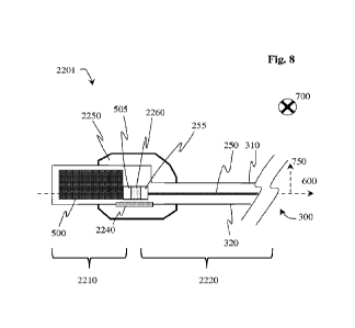
FIG. 8 is a transverse view of a further implementation of an implantable
stimulator consistent with certain embodiments of the present invention.
FIG. 9 is a transverse view of a further implementation of an implantable
stimulator consistent with certain embodiments of the present invention.
FIG. 10A to 1OF are bottom views of implementations of a mechanical brace
consistent with certain embodiments of the present invention.
FIG. 11A, FIG. 11B and FIG. 11C depict cross-sections through improved
implantable electrical devices.
FIG. 12A and FIG. 12B depict cross-sections through improved implantable
medical devices comprising an improved implantable electrical device, and one
or more
electrodes.
FIG. 13A is a bottom view of a further implementation of an implantable
stimulator consistent with certain embodiments of the present invention.
FIG. 13B is a transverse view of a further implementation of an implantable
stimulator consistent with certain embodiments of the present invention.
FIG. 14A is a transverse view of a further implementation of an implantable
stimulator consistent with certain embodiments of the present invention.
FIG. 14B is a bottom view of a further implementation of an implantable
stimulator consistent with certain embodiments of the present invention.
FIG. 15 presents measurement results comparing the average pull force , dry
and
after soaking, of LCP coated with PDMS using different processes.
DETAILED DESCRIPTION
While this invention is susceptible of embodiment in many different forms,
there
is shown in the drawings and will herein be described in detail specific
embodiments,
with the understanding that the present disclosure of such embodiments is to
be
considered as an example of the principles and not intended to limit the
invention to the
11
CA 03226804 2024- 1-23
WO 2023/026216
PCT/IB2022/057941
specific embodiments shown and described. The embodiments described, and their
detailed construction and elements, are merely provided to assist in a
comprehensive
understanding of the invention. The scope of the invention is best defined by
the
appended claims. In the description below, like reference numerals are used to
describe
the same, similar or corresponding parts in the several views of the drawings
or even in
different drawings.
Thus, it is apparent that the present invention can be carried out in a
variety of
ways, and does not require any of the specific features described herein.
Also, well-
known functions or constructions are not described in detail since they would
obscure the
invention with unnecessary detail. Any signal arrows in the drawings/figures
should be
considered only as exemplary, and not limiting, unless otherwise specifically
noted,
It will be understood that, although the terms first, second, etc. may be used
herein
to describe various elements, these elements should not be limited by these
terms. These
terms are only used to distinguish one element from another. For example, a
first element
could be termed a second element, and, similarly, a second element could be
termed a
first element, without departing from the scope of example embodiments. As
used herein,
the term "and/or" includes any and all combinations of one or more of the
associated
listed items. As used herein, "at least one of A, B, and C" indicates A or B
or C or any
combination thereof. As used herein, the singular form of a word includes the
plural, and
vice versa, unless the context clearly dictates otherwise.
The terms "a" or "an", as used herein, are defined as one or more than one.
The
term "plurality", as used herein, is defined as two or more than two. The term
"another",
as used herein, is defined as at least a second or more. The terms "including"
and/or
-having", as used herein, are defined as comprising (i.e., open language). The
term
"coupled", as used herein, is defined as connected, although not necessarily
directly, and
not necessarily mechanically.
It should also be noted that in some alternative implementations, the
functions/acts
noted may occur out of the order noted in the figures. For example, two
figures shown in
succession may in fact be executed substantially concurrently or may sometimes
be
executed in the reverse order, depending upon the functionality/acts involved.
As used herein, ranges are used herein in shorthand, so as to avoid having to
list
and describe each and every value within the range. Any appropriate value
within the
range can be selected, where appropriate, as the upper value, lower value, or
the terminus
12
CA 03226804 2024- 1-23
WO 2023/026216
PCT/IB2022/057941
of the range.
The words "comprise", "comprises", and "comprising" are to be interpreted
inclusively rather than exclusively. Likewise the terms "include", "including"
and "or"
should all be construed to be inclusive, unless such a construction is clearly
prohibited
from the context. The terms "comprising" or "including" are intended to
include
embodiments encompassed by the terms "consisting essentially of' and -
consisting of'.
Similarly, the term "consisting essentially of' is intended to include
embodiments
encompassed by the term "consisting of'. Although having distinct meanings,
the terms
"comprising", "having", "containing' and "consisting of' may be replaced with
one
another throughout the description of the invention.
"About" means a referenced numeric indication plus or minus 10% of that
referenced numeric indication. For example, the term "about 4" would include a
range of
3.6 to 4.4. All numbers expressing quantities of ingredients, reaction
conditions, and so
forth used in the specification are to be understood as being modified in all
instances by
the term "about." Accordingly, unless indicated to the contrary, the numerical
parameters
set forth herein are approximations that can vary depending upon the desired
properties
sought to be obtained. At the very least, and not as an attempt to limit the
application of
the doctrine of equivalents to the scope of any claims, each numerical
parameter should
be construed in light of the number of significant digits and ordinary
rounding
approaches.
Wherever the phrase "for example," "such as," "including" and the like are
used
herein, the phrase "and without limitation" is understood to follow unless
explicitly stated
otherwise.
"Typically" or "optionally" means that the subsequently described event or
circumstance may or may not occur, and that the description includes instances
where
said event or circumstance occurs and instances where it does not.
Reference throughout this document to "one embodiment", "certain
embodiments", "an embodiment" or similar terms means that a particular
feature,
structure, or characteristic described in connection with the embodiment is
included in at
least one embodiment of the present invention. Thus, the appearances of such
phrases or
in various places throughout this specification are not necessarily all
referring to the same
embodiment. Furthermore, the particular features, structures, or
characteristics may be
combined by a person skilled in the art in any suitable manner in one or more
13
CA 03226804 2024- 1-23
WO 2023/026216
PCT/IB2022/057941
embodiments without limitation.
In the following detailed description, numerous non-limiting specific details
are
given to assist in understanding this disclosure.
FIG. 1A, 1B & 1C depict longitudinal cross-sections through a first embodiment
100 of an implantable stimulator comprising:
- a pulse generator 500 (only depicted in FIG. 1B and 1C) for generating at
least
one electrical treatment stimulation pulse; and
- a conformable portion of a foil-like substrate 300 having a longitudinal
axis 600
extending from the pulse generator 500 to a distal end of the substrate 300.
The substrate
300 comprises one or more adjacent polymeric substrate layers and has a first
310 and a
second 320 planar (outer) surface.
The implantable stimulator 100 also comprises:
- an electrode array 200, 400, proximate the distal end, having at least
one
electrode of a first 200a, 200b type and at least one electrode of a second
type 400a, 400b.
The electrodes 200, 400 are comprised in the first 310 or second 320 surface,
and each is
configurable for transferring treatment energy, in use, to (as a stimulation
electrode)
and/or from (as a return electrode) human or animal tissue. In this context,
an array may
be considered a systematic arrangement of two or more electrodes 200a, 200b,
400a,
400b. 1D, 2D or 3D arrays may be provided. Optionally, they may be arranged in
rows
and/or columns.
The implantable stimulator 100 further comprises:
- one or more electrical interconnections 250, between the pulse generator
500 and
the first 200a, 200b and the second 400a, 400b electrodes, for transferring
electrical
energy as one or more electrical treatment stimulation pulses to the coupled
first
electrodes 200a, 200b and/or the second electrodes 400a, 400b. The one or more
electrical
interconnections 250 are comprised (or positioned) between the first surface
310 and the
second 320 surfaces. A plurality of electrical interconnections 250 is
considered to be
two, or more than two, electrical interconnections 250.
In this disclosure, the conformability of the electrode array 200, 400 is
determined
to a high degree by the one or more of the following:
- the conformability of a portion of the substrate 300 proximate the
electrodes 200,
300;
- the arrangement and positions of the electrodes 200, 400;
14
CA 03226804 2024- 1-23
WO 2023/026216
PCT/IB2022/057941
- the materials and dimensions (or extent) of the materials comprised in
the
electrodes 200, 400;
- the arrangement and positions of the one or more interconnections 250
proximate the electrodes 200, 400; and
- the materials and dimensions (or extent) of the materials comprised in the
interconnections 200, 400.
By suitable configuration, arrangement and optimization, an implantable
electrode
array 200, 400 may be provided which is foil-like (or film-like) and highly
conformable.
As depicted, the conformable portion of the foil-like substrate 300 is
preferably
elongated along the longitudinal axis 600, having a tape-like shape, allowing
the pulse
generator 500 to be disposed (or located) further away from the position of
the electrodes
200, 400.
If the substrate 300 is substantially planar (in a non-limiting example, by
allowing
the substrate 300 to conform to a planar surface), the first 310 and second
320 surfaces
are disposed along substantially parallel transverse planes 600, 700. As
depicted in FIG.
1A, the first surface 310 lies in a plane comprising the longitudinal axis 600
and a first
transverse axis 700 ¨ the first transverse axis 700 is substantially
perpendicular to the
longitudinal axis 600. As depicted in FIG. 1A, the plane of the first surface
310 is
substantially perpendicular to the plane of the cross-section drawing
(substantially
perpendicular to the surface of the paper).
The conformable portion of the foil-like substrate 300 has a maximum thickness
of 0.5 millimeter or less, proximate the first 200a, 200b and second 400a,
400b
electrodes, the thickness being defined by the first 310 and second surfaces
320 ¨ it may
be determined by a perpendicular distance between conesponding points on the
first 310
and second planar surfaces 320. This is preferably determined when the
substrate 300
conforms to a planar surface.
The foil-like substrate 300 has a thickness or extent along a second
transverse axis
750 ¨ this second transverse axis 750 is substantially perpendicular to both
the
longitudinal axis 600 and the first transverse axis 700 ¨ it lies in the plane
of the drawing
(along the surface of the paper) as depicted. The first surface 310 is
depicted as an upper
surface and the second surface 320 is depicted as a lower surface.
The thickness may therefore be determined by a perpendicular distance along
the
second transverse axis 750 between corresponding points on the first 310 and
second
CA 03226804 2024- 1-23
WO 2023/026216
PCT/IB2022/057941
planar surfaces 320. The maximum thickness of the conformable portion of the
foil-like
substrate 300 proximate the first 200a, 200b and second 400a, 400b electrodes
is 0.5mm
or less, preferably 0.3 millimeters or less, even more preferably 0.2
millimeters or less,
yet more preferably 0.1 millimeters or less.
In general, the lower the maximum thickness (in other words, the thinner the
substrate), the higher the degree of conformance. However, a higher maximum
thickness
may be preferred to improve mechanical strength.
To clarify the differences between the different views depicted, the axes are
given
nominal directions:
- the longitudinal axis 600 extends from the proximal end (not depicted in
FIG.
1A, but depicted in FIG. 1B and 1C) on the left, to the distal end, depicted
on the right of
the page;
- the first transverse axis 700 extends into the page as depicted; and
- the second transverse axis 750 extends from bottom to top as depicted.
The conformable portion of the foil-like substrate 300 may be configured and
arranged as a multilayer ¨ it comprises two or more adjacent polymeric
substrate layers
secured to each other, and having the first 310 and second 320 planar surface.
The one or
more electrical interconnections 250 are also comprised (or positioned)
between the first
310 and second 320 planar surfaces. However, it is not necessary that the two
or more
polymeric layers and/or interconnections have similar extents along the first
transverse
axis 700. In other words, within the context of this disclosure, there may be
regions where
an interconnection 250 is sandwiched between regions of polymeric substrate
(appears as
a multilayer in a longitudinal cross-section), adjacent to regions where the
polymeric
substrate is substantially contiguous. Similarly, there may be regions where
an
interconnection 250 is sandwiched between two polymeric substrate layers
(appears as a
multilayer in a longitudinal cross-section), adjacent to regions where the
substrate
comprises two adjacent substrate layers. Similarly, a substrate comprising two
or more
polymeric substrate layer may be modified (physically and/or chemically), such
that it
appears to be one layer of polymeric substrate.
These polymeric substrate layers are selected for suitability to be
conformable,
and to comprise the one or more electrical interconnections 250. Preferably,
the polymeric
substrate materials are also biocompatible and durable, such as a material
selected from
the group comprising silicone rubber, siloxane polymers,
polydimethylsiloxanes,
16
CA 03226804 2024- 1-23
WO 2023/026216
PCT/IB2022/057941
polyurethane, polyether urethane, polyetherurethane urea, polyesterurethane,
polyamide,
polycarbonate, polyester, polypropylene, polyethylene, polystyrene, polyvinyl
chloride,
polytetrafluoroethylene, polysulfone, cellulose acetate,
polymethylmethacrylate,
polyethylene, and polyvinylacetate. Suitable polymer materials, including LCP
(Liquid
Crystal Polymer) films, are described in "Polymers for Neural Implants",
Hassler,
Boretius, Stieglitz, Journal of Polymer Science: Part B Polymer Physics, 2011,
49, 18-33
(DOT 10.1002/polb.22169), In particular, Table 1 is included here as
reference, depicting
the properties of Polyimide (UBE U-Varnish-S), Parylene C (PCS Parylene C),
PDMS
(NuSil MED-1000), SU-8 (MicroChern SU-8 2000 & 3000 Series), and LCP (Vectra
MT1300).
Conformable foil-like substrates 300 are configured to follow the contours of
the
underlying anatomical features very closely by being flexible. Very thin foil-
like
substrates 300 have the additional advantage that they have increased
flexibility.
Most preferably, the polymeric substrate layers comprise an LCP, Parylene
and/or
a Polyimide. LCP's are chemically and biologically stable thermoplastic
polymers which
allow for hermetic sensor modules having a small size and low moisture
penetration.
Advantageously, an LCP may be thermoformed allowing complex shapes to be
provided. Very thin (and subsequently very conformable) and very flat (highly
planar)
layers of an LCP may be provided. For fine tuning of shapes, a suitable laser
may also be
used for cutting.
In a non-limiting example, a conformable foil-like substrate 300 of LCP may
have
a thickness (extent along the second transverse axis 750) in the range 50
microns (urn) to
720 microns (urn), preferably 100 microns (um) to 300 microns (um). In an
exemplary
embodiment, values of 150 um (micron), 100um, 50um, or 25um may be provided.
When conforming to a substantially planar surface, the foil-like surface 300
is
substantially comprised in a plane with a transverse extent substantially
perpendicular to
the longitudinal axis 600, wherein the planar width may be determined by a
perpendicular
distance between corresponding points on outer surfaces edges of the planar
foil-like
substrate 300 along the transverse extent. As depicted, this is along the
first transverse
axis 700. In an embodiment, electrode 200, 400 widths of 2 mm to 20 mm may be
provided using LCP.
At room temperature, thin LCP films have mechanical properties similar to
steel.
This is important as implantable substrates 300 should be strong enough to be
implanted,
17
CA 03226804 2024- 1-23
WO 2023/026216
PCT/IB2022/057941
strong enough to be removed (explanted) and strong enough to follow ally
movement of
the neighboring anatomical features and/or structures without deteriorating.
LCP belongs to the polymer materials with the lowest permeability for gases
and
water. LCP's can be bonded to themselves, allowing multilayer constructions
with a
homogenous structure.
In contrast to LCP's, polyimides are thermoset polymers, which require
adhesives
for the construction of multilaycr portions with electrode arrays. Polyimides
are thermoset
polymer material with high temperature and flexural endurance.
In an embodiment, an LCP may be used to provide a conformable substrate 300 as
a multilayer ¨ in other words, two or more adjacent polymeric substrate
layers. In a non-
limiting example, these may be layers of 25 um (micron) thickness.
In an embodiment, one or more electrical interconnections 250 may be provided
(or positioned) between the first 310 and second 320 surfaces by
metallization. These
may be conductors embedded in the substrate 300 such as by having a single
polymer
layer and applying conductive material using suitable deposition techniques
known from
the semiconductor industry.
In an embodiment, if two or more adjacent polymeric substrate layers are
provided, an interconnection layer may be provided using suitable techniques
such as
those from the semiconductor industry. The polymeric substrate layers may also
be
considered adjacent when one of more adhesion layers are used between them.
Examples
of suitable adhesion materials and adhesion layers are described below in
relation to FIG.
11 to FIG. 12.
In an embodiment, lamination may also be used to provide a substrate 300 with
the desired physical and chemical properties, and/or to provide a convenient
method of
manufacture. In a non-limiting example, a substrate 300 may comprise three
laminated
polymer layers: two high temperature thermoplastic layers with a low-
temperature layer
(bond-ply) in between, and high-temperature layers towards the first surface
310 and
second surface 320.
In an alternative embodiment, two layers of silicone may be provided as
polymeric substrate layers: one layer of silicone is provided, metal is
patterned on one of
its outer surfaces, and a second layer of silicone is added over the metal
patterning by
jetting, over-molding, or spin-coating.
In an embodiment, the electrical interconnections 250 may comprise one or more
18
CA 03226804 2024- 1-23
WO 2023/026216
PCT/IB2022/057941
conductive materials, such as a metal, formed as required in one or more
conductive
elements: wire, strand, foil, lamina, plate, and/or sheet. They may be a
substantially
contiguous (one conductor). They may also comprise more than one conductor,
configured and arranged to be, in use, electrically connected with each other
¨ in other
words, the one or more conductors are configured and arranged to be
substantially
electrically contiguous in use.
Alternatively, the one or more electrical interconnections 250 may be
comprised in
one or more conductive interconnection layers 250, the one or more conductive
interconnection layers being comprised (or positioned) between two adjacent
polymeric
substrate layers. As depicted in HG. 1A, a plurality of interconnections may
be provided
at different dispositions (or depths or positions) between the first surface
310 and the
second surface 320.
In an embodiment, an interconnection 250 in the context of this disclosure is
not
configured or arranged to be, in use, in contact with human or animal tissue.
The one or
more interconnections 250 are embedded (or covered) in one or more layers of a
low
conductance or insulating polymer, such as LCP. Additionally or alternatively,
one or
more encapsulation layers may be used.
One or more interconnection layers 250 may also be provided by metallization
using techniques from the PCB (Printed Circuit Board) industry, such as
metallization
with a bio-compatible metal such as gold or platinum. Electro-plating may be
used.
Layers comprising LCP films are particularly suitable for metallization. These
electrical
interconnections 250 and/or interconnect layers 250 are configured to transfer
electrical
energy as one or more electrical treatment stimulation pulses from the pulse
generator
500 to the coupled first electrodes 200a, 200b and/or the second electrodes
400a, 400b.
Using suitable polymeric substrate materials, such as an LCP film, allows the
conformable portions of the foil-like (or film-like) substrate 300 and
electrode array 200,
300 to have a high width-to-height ratio, providing a bio-compatible
electronic foil (or
film), or bio-electronic foil (or film).
In an embodiment, when the substrate 300 conforms to a substantially planar
surface, the ratio of maximum planar width to maximum thickness proximate the
first
200a, 200b and second 400a, 400b electrodes may be 7:1 or higher, preferably
10:1 or
higher, more preferably 15:1 or higher, yet more preferably 30:1 or higher,
even more
preferably 50:1 or higher.
19
CA 03226804 2024- 1-23
WO 2023/026216
PCT/IB2022/057941
Ratios of 100:1 or higher may also be advantageous, and may he provided using
one or more mechanically strong substrate layers of an LCP film, with a width
of
approximately 20mm and a thickness of approximately 0.2 mm. This provides a
high
degree of flexibility, and therefore also a high degree of conformability.
Additional
measures may also be taken to increase the degree of conformability in the
first transverse
direction 700, such as varying the width of the substrate, adding one or more
undulations
and/or providing bending points.
In a non-limiting example, when using a single row of electrodes 200, 400
and/or
electrodes 200, 400 with a smaller width, the width may be four mm with a
thickness of
approximately 0.2mm ¨ this is a ratio of approximately 20:1.
In a non-limiting example, in a portion of the substrate proximate the pulse
generator 500, greater extents may be required which further depend, to a high
degree, on
the dimensions of the electronic components used a width of twenty mm and a
thickness
of three mm. This is a ratio of approximately 6.67:1.
As depicted in FIG. IA, the distal end (or distal portion) of the conformable
foil-
like substrate 300 comprises:
- two electrodes 200a, 200b of a first type, comprised in the first surface
310, and
- two electrodes 400a, 400b of a second type, also comprised in the first
surface
310. From proximal to distal end, the order depicted is 200a, 400a, 200b, 400b
¨ in other
words, each electrode of the first type 200a, 20011 is proximate an electrode
of the second
type 400a, 400b and comprised in the same surface 310.
The foil-like substrate 300 comprises an electrical interconnection 250
between
each electrode 200a, 400a, 200b, 400b and the pulse generator. In this
embodiment, each
electrical interconnection 250 is configured and arranged such that each
electrode 200a,
400a, 200b, 400b is electrically connected substantially independently ¨
consequently,
one of the operating modes available by suitably configuring the pulse
generator 500 is
substantially independent operation. The pulse generator 500 may be configured
using
one or more hardware, firmware and/or software parameters.
Although depicted in FIG. 1A as individual connections 250 at different
distances
(or positions) between the first 310 and second 320 surfaces, the skilled
person will also
realize that the same interconnections may be provided by a suitably
configured
interconnections 250 (or an interconnection layer 250) at approximately the
same distance
(or position) between the first 310 and second 320 surfaces, similar to the
embodiment
CA 03226804 2024- 1-23
WO 2023/026216
PCT/IB2022/057941
depicted in FIG. 3B, and described below.
-Comprised in" the first 310 or second 320 surface means that the electrodes
200a,
400a, 200b, 400b are relatively thin (such as when the substrate is arranged
to conform to
a substantially planar surface, it may have an extent along the second
transverse axis of
20 to 50 microns or less. Thinner electrodes may also be used to further
increase the
degree of conformability, such as 1 micron or less), and attached to (or at
least partially
embedded in) the surface.
The electrodes 200, 400 may comprise a conductive material such as gold,
platinum, platinum black, TiN, Ir0/, iridium, and/or platinum/iridium alloys
and/G[-
oxides. Conductive polymers, such as Pedot, may also be used. Preferably, bio-
compatible conductive materials are used. PCB/metallization techniques may be
used to
manufacture them on or in the first 310 and/or second 330 surfaces of the one
or more
polymeric substrate layers.
Thicker metal layers are generally preferred over thinner metal layers for
electrodes 200a, 200b, 400a, 400b because they can be subjected to bodily
substances that
may dissolve the metal. However, thicker metal layers typically increase
rigidity (reduce
conformability) proximate the thicker layer.
The stimulator 100 may be implanted by first creating a subcutaneous tunnel
and/or using an implantation tool. However, the high degree of conformability
may make
successful implantation more difficult. Even when using a suitable insertion
tool, the
electrode positions may be found later to be incorrect due to misalignment,
lead migration
during implantation, or lead migration after transplantation.
At least the distal end comprising the electrode array 200, 400, is implanted.
However, it may be advantageous to implant the stimulator 100.
In addition, during implantation, it may be difficult to precisely identify
the
desired position for the stimulation. When implanted, the stimulator
electrodes should be
positioned sufficiently close to the nerve to be stimulated. But nerve
pathways may not
always be clearly visible to the professional performing the implantation, and
the
disposition and path of the nerve pathways vary greatly from person-to-person.
As depicted in FIG. 1, there is no substantial hardware difference between the
first-type 200a, 200b and second type 400a, 400b electrodes ¨ any difference
in
functionality is determined in this implementation mainly by the configuration
(one or
more hardware, firmware and/or software parameters) of the pulse generator
500. There
21
CA 03226804 2024- 1-23
WO 2023/026216
PCT/IB2022/057941
may be a smaller influence on the electrical properties due to the arrangement
and routing
of the interconnections 250.
One or more coupled electrodes of the same type 200a, 200b or 400a, 400b may
be operated substantially the same by suitable configuration of the pulse
generator 500 -
in other words, the stimulation energy applied to the electrodes 200, 400 is
substantially
the same at substantially the same time instance (usually measured as a
voltage, a current,
a power, a charge, or any combination thereof). This may also be used to
anticipate and/or
correct for a misalignment and/or lead migration ¨ this is advantageous as it
allows the
configuration to be performed at least partially using software.
Additionally or alternatively, two or more electrodes 200, 400 may be
configured
and arranged using one or more parameters of the pulse generator 500 as a
stimulation
electrode or a return electrode. This may provide a higher degree of
configurability as it
only becomes necessary to implant the substrate 300 such that at least two of
the
electrodes are proximate the desired stimulation location.
In this embodiment 100, the electrodes of the first type 200a, 200b are
nominally
configured and arranged to be operated as a stimulation electrode.
The electrodes of the second type 400a, 400b are nominally configured to be
operated as a return electrode ¨ each is configured to provide, in use, an
electrical return
for one or more stimulation electrode 200a, 200b. In other words, the
electrical return
400a, 400b closes the electrical circuit. It may also be similarly configured
to provide an
electrical ground for a corresponding electrical energy source.
Three configurations are thus provided based on this nominal configuration:
either:
- a stimulation / return electrode pair 200a / 400a proximate the first
surface 310 at
that stimulation / return location; or
- a stimulation / return electrode pair 200b / 400b proximate the first
surface 310
at that stimulation / return location; or
. a combination thereof.
In an embodiment, one or more stimulation electrodes 200a, 200b may be
provided in such a stimulator 100. The number, dimensions and/or spacings of
the
stimulating electrodes 200a, 200b may be selected and optimized depending on
the
treatment. In an embodiment, if more than one stimulation electrode 200a, 200b
is
provided, each stimulation electrode 200a, 200b may provide:
22
CA 03226804 2024- 1-23
WO 2023/026216
PCT/IB2022/057941
- a different stimulation effect, a similar stimulation effect or the same
stimulation
effect.
To avoid a misalignment, a selection may be made of one or two electrodes
200a,
200b proximate the tissues where the effect is to be created.
Two or more stimulation electrodes 200a, 200b may be made active at
substantially the same time if stimulation over a larger area is required
and/or at a
location between the active stimulation electrodes 200a, 200b.
In an embodiment, a stimulation electrode 200a, 200b may have dimensions in
the
order of six to eight mm along the longitudinal axis 600, and three to five mm
along the
first transverse axis 700, so approximately 18 to 40 square mm (mm2).
In an embodiment, a foil-like substrate 300, suitable for an implantable
stimulator,
may comprise up to twelve stimulation 200a, 200b and return 400a, 400b
electrodes over
a length of 15cm to allow for a correction for misalignment, or to simply
allow the
specialist to select the most effective stimulation location.
In an embodiment, FIG. 1B depicts a view of the second surface 320 of the
implantable distal end (or portion) of the foil-like substrate 300 depicted in
FIG. 1A. In
other words, the second surface 320 is depicted in the plane of the paper,
lying along the
longitudinal axis 600 (depicted from bottom to top) and in the first
transverse axis 700
(depicted from left to right). The second transverse axis 750 extends into the
page. The
first surface 310 is not depicted in FIG. 1B, hut lies at a higher position
along the second
transverse axis 750 (into the page), and is also substantially parallel to the
plane of the
drawing. The foil-like substrate 300 is arranged to conform to a substantially
planar
surface.
The pulse generator 500 may be disposed (or positioned) between the second 320
surface and the first 310 surface. In FIG. 1B and 1C, it is depicted with
dotted lines.
Alternatively, the pulse generator 500 may be at least partially disposed on
the first
surface 310 or on the second surface 320. Alternatively, the pulse generator
500 may be at
least partially embedded in the first surface 310 or in the second surface
320.
Depending on the degree of embedding and the one or more electrical components
used for the pulse generator 500, the maximum thickness may be optimized.
Components
may be thinned to minimize the thickness. If the substrate 300 is configured
and arranged
to be conformable and/or foil-like, the maximum thickness of the implantable
stimulator
100 in a portion of the substrate proximate the pulse generator 500 may be
five
23
CA 03226804 2024- 1-23
WO 2023/026216
PCT/IB2022/057941
millimeters or less, preferably four millimeters or less, even more preferably
three
millimeters or less, the thickness being determined by a perpendicular
distance between
corresponding points on outer planar surfaces when the implantable stimulator
100
conforms to a substantially planar surface. Additional optional electrical
components,
such as an antenna, comprising a coil or dipole or fractal antenna, may also
influence the
thickness depending on the degree that they are embedded in the substrate.
The stimulator 100 and the foil-like substrate 300 extend along the first
transverse
axis 700 (considered the planar width of the stimulator 100 / foil-like
substrate 300 when
conforming to a substantially planar surface). As depicted, the planar width
in a portion of
the substrate proximate the pulse generator 500 may be greater than the planar
width in
another portion of the substrate proximate the electrodes 200a, 200b, 400a,
400b at the
distal end (or portion) of the foil-like substrate 300. The planar width
proximate the pulse
generator 500 may depend on the hardware and components used for the pulse
generator
500 ¨ typically, it is at least the width of the integrated circuit used for
the pulse generator
500. Additional optional electrical components, such as an antenna comprising
a coil or
dipole or fractal antenna, may also influence the planar width.
In an embodiment, the planar width proximate the electrodes 200a, 200b, 400a,
400b may depend on the conductors used for the electrodes 200a, 200b, 400a,
400b and
the one or more interconnections 250. In an embodiment, the planar width is at
least the
width of the first electrode 200a, 200h or the second electrode 400a, 400h.
In an embodiment, FIG. 1C depicts a view of the first surface 310 of the
implantable distal end (or portion) of the foil-like substrate 300 depicted in
FIG. 1A and
1B. In other words, the first surface 310 is depicted in the plane of the
paper, lying along
the longitudinal axis 600 (depicted from bottom to top) and in the first
transverse axis 700
(depicted from right to left). The second transverse axis 750 extends out of
the page. This
is the view facing the animal or human tissue which is stimulated (in use).
The second
surface 320 is not depicted in FIG. 1C, but lies at a lower position along the
second
transverse axis 750 (into the page), and is also substantially parallel to the
plane of the
drawing. The foil-like substrate 300 is arranged to conform to a substantially
planar
surface.
The one or more interconnections 250 are disposed (or positioned) between the
first 310 surface and the second 320 surface, as depicted in FIG. 1A. In FIG.
1C, they are
depicted as dotted lines, representing the interconnections 250 (or suitably
configured one
24
CA 03226804 2024- 1-23
WO 2023/026216
PCT/IB2022/057941
or more interconnection layers 250) that have been provided for each of the
electrodes
200a, 200b, 400a, 400b in this embodiment. A single dotted line 250 is
depicted between
the pulse generator 500 and the electrodes 200, 400 to indicate, in embodiment
100, that
the interconnections 250 are at approximately the same disposition along the
first
transverse axis 700.
As depicted in FIG. 1C, the electrodes 200a, 200b, 400a, 400b each have a
longitudinal extent (length) along the longitudinal axis 600 and a transverse
extent
(width) along the first transverse axis 700.
Although depicted as similar, in practice, each electrode 200a, 200b, 400a,
400b
may vary in shape, transverse cross-section, orientation and/or size (or
extent), depending
on the intended use and/or the desired degree of configurability.
After implantation of the stimulator 100, or at least of the distal end (or
portion)
comprising the electrode array 200, 400, the pulse generator 500 may be
configured and
arranged to provide, in use, electrical energy to the one or more coupled
electrodes of the
first type 200a, 200b with respect to the electrical return applied to the one
or more
coupled electrodes of the second type 400a, 400b.
The configurability of the stimulator 100 allows, before, during and/or after
implantation of at least of the distal end (or portion) comprising the
electrode array 200,
400, the operation of the one or more electrodes 200a, 200b, 400a, 400b to be
determined
and/or adapted. The operation may also be reconfigured one or more times
during the
period that the stimulator 100 is implanted to optimize and/or prolong
treatment.
In an embodiment, the pulse generator 500 may be initially configured to
nominally operate 200a and 400a as respectively a stimulation / return
electrode pair.
After implantation of at least the distal end 200, 400, insufficient
stimulation may be
observed and/or measured. If it is assumed to be due to a mainly longitudinal
misalignment, the pulse generator 500 may be alternatively configured, using
one or more
parameters, to nominally operate 200b and 400b as respectively a stimulation /
return
electrode pair.
The stimulator 100 may be further configured and arranged to switch the pulse
generator 500 under predetermined and/or controlled conditions between these
configurations. It may be convenient to further consider these configurations
as a first and
second electrode modes, and allow a user to select a mode as a preference
and/or switch
mode. Alternatively, the pulse generator 500 may switch modes under
predetermined
CA 03226804 2024- 1-23
WO 2023/026216
PCT/IB2022/057941
and/or controlled conditions.
Additionally or alternatively, other modes may also be provided for
configuring
the pulse generator 500 to operate in:
- a first electrode mode, wherein electrical stimulation energy is provided
to one or
more coupled electrodes of the first type 200a, 200b as one or more electrical
treatment
stimulation pulses, the one or more coupled electrodes of the second type
400a, 400b
being configured to provide, in use, a corresponding electrical return for the
one or more
first electrodes 200a; 200b; or
- a second electrode mode, wherein energy is provided to one or more
coupled
electrodes of the second type 400a, 400b as one or more electrical treatment
stimulation
pulses, the one or more coupled electrodes of the first type 200a, 200b being
configured
to provide, in use, a corresponding electrical return for the one or more
second electrodes
400a, 400b.
Again, the stimulator 100 may be further configured and arranged to switch the
pulse generator 500 under predetermined and/or controlled conditions between
these
configurations or modes. Additionally or alternatively, a user may be allowed
to select a
mode as a preference and/or switch mode.
The skilled person will realize that the electrodes 200a, 200b, 400a, 400b may
be
configured to operate in more complex configurations, such as:
- 400a and 200a rn ay be operated as respectively a stirnul anon / return
electrode
pair (reversing the original intended operation);
- 400b and 200b may be operated as respectively a stimulation / return
electrode
pair;
- if an intermediate stimulation is preferred, two or more electrodes 200a,
200b,
400a, 400b may be operated substantially simultaneously as one or more
stimulation
electrodes;
- one or more electrodes 200a, 200b, 400a, 400b may be operated as one or
more
return electrodes,
- electrode 400a operated as a stimulation electrode, in combination with
electrode
200a and electrode 200b as return electrodes;
- electrode 400a and 200b operated as a stimulation electrode, in
combination with
electrode 200a and electrode 400b as a return electrode.
Alternatively or additionally, the shape, orientation, transverse cross-
section,
26
CA 03226804 2024- 1-23
WO 2023/026216
PCT/IB2022/057941
and/or size (or length) of one or more stimulation electrodes may be
differently
configured compared to one or more return electrodes.
A number of parameters and properties may be considered when configuring and
arranging a portion of the foil-like substrate 300 proximate the electrode
array 200, 400
for conformability, such as:
- the transverse 700 and/or longitudinal extent 600 of the one or more
electrodes
200a, 200b, 400a, 400b
- the thickness of the foil-like substrate 300, or the perpendicular
distance between
the first surface 310 and the second surface 320
- the materials comprised in the foil-like substrate 300, and their physical
properties
- the number and extent of interconnections 250 and/or interconnection
layers 250
between the first surface 310 and second surface 320.
There have been attempts to make traditional leads, such as cylindrical leads,
much thinner to allow subcutaneous implantation and/or to increase comfort by
flattening.
But the surface area of the flattened electrodes may become disadvantageously
small.
In a non-limiting example, a conventional 0.2mm round lead with 1 cm long
electrodes is estimated to result in an electrode with approximately 6 mm2
electrode
surface.
However, using the conformable electrode arrays described herein, a thin
substrate
300 with dimensions of 0.2 mm thick, and four mm wide may be configured and
arranged
to provide approximately 35 mm2 electrode surface in the same length. It is
estimated that
this may reduce impedance by a factor of approximately 35/6, and reduce power
consumption by approximately 35/6.
In an embodiment, FIG. 2A, 2B and 2C depict longitudinal cross-sections
through
a second embodiment 101 of an implantable stimulator. it is similar to the
first
embodiment 100, depicted in FIG. 1A, 1B and 1C except:
- instead of four electrodes comprised in the first surface 310, this
embodiment
comprises two electrodes in the first surface 310 ¨ nominally an electrode of
the first type
200a and nominally an electrode of the second type 400a. From proximal to
distal end,
the order depicted is 200a, 400a ¨ in other words, an electrode of the first
type 200a is
proximate an electrode of the second type 400a in the first surface 310.
- the distal end of the stimulator 101 also comprises two electrodes in the
second
27
CA 03226804 2024- 1-23
WO 2023/026216
PCT/IB2022/057941
surface 320 ¨ a further electrode nominally of the first type 200b and a
further electrode
nominally of the second type 400b. From proximal to distal end, the order
depicted is
200b, 400b ¨ in other words, an electrode of the first type 200b is proximate
an electrode
of the second type 400b in the second surface 320.
- In Fig. 2B, the view of the second surface 320 depicts the two electrodes
200a,
400a comprised in that surface, and one or more interconnections 250 are
depicted using
a dotted line;
- In Fig. 2C, the view of the second surface 320 depicts the two electrodes
200b,
400b comprised in that surface, and one or more interconnections 250 are
depicted using
a dotted line;
In this embodiment 101, the electrodes of the first type 200a, 200b are
nominally
configured and arranged to be operated as a stimulation electrode, and the
electrodes of
the second type 400a, 400b are nominally configured to be operated as a return
electrode.
Three main configurations are thus provided:
- a stimulation / return electrode pair 200a / 400a proximate the first
surface 310;
Or
- a stimulation / return electrode pair 200b / 400b proximate the second
surface
320; or
- a combination thereof.
This may be advantageous if it is uncertain whether the implantable distal end
of
the foil-like substrate 300 may be "above" or "below" the targeted tissue such
as "above"
or "below" a nerve. This may be determined after implantation by attempting
stimulation
in each nominal configuration and observing and/or measuring the presence of
neural
stimulation.
As discussed above, in relation to FIG. 1A, 1B and 1C, each electrode 200a,
200b,
400a, 400b may be operated as one or more stimulation electrodes or operated
as one or
more return electrodes.
In an embodiment, FIG. 3A, 3B and 3C depict longitudinal cross-sections
through
a third embodiment 102 of an implantable stimulator. It is similar to the
second
embodiment 101, depicted in FIG. 2A, 2B and 2C except:
- interconnections 250 are disposed at approximately the same disposition
along
the second transverse axis 750, as depicted in FIG. 3A. The lines 250 are
hatched to
indicate that they are not depicted as being in the same longitudinal cross-
section ¨ there
28
CA 03226804 2024- 1-23
WO 2023/026216
PCT/IB2022/057941
are interconnections 250 disposed at substantially different positions along
the first
transverse axis 700;
- interconnections 250 are disposed at substantially different dispositions
along the
first transverse axis 700, as depicted in FIG. 3B and 3C as two adjacent
dashed lines
between the electrode array 200, 400 and the pulse generator 500;
- instead of nominally comprising an electrode of the first 200 and second
type
400 in the first surface 310, the first surface 310 comprises a first 200a and
second 200b
electrode nominally of the first type 200;
- instead of nominally comprising an electrode of the first 200 and second
type
400 in the second surface 320, the second surface 320 comprises a first 400a
and second
400b electrode nominally of the second type 400;
In this embodiment 102, the electrodes of the first type 200a, 200b are
nominally
configured and arranged to be operated as a stimulation electrode, and the
electrodes of
the second type 400a, 400b are nominally configured to be operated as a return
electrode.
Three main configurations are thus provided:
- a stimulation / return electrode pair 200a / 400a for stimulating between
the first
surface 310 and second surface 320 proximate the location of this electrode
pair; or
- a stimulation / return electrode pair 200b / 400b for stimulating between
the first
surface 310 and second surface 320 proximate the location of the electrode
pair; or
- a combination thereof.
This may be advantageous to correct for a longitudinal misalignment, or to
simply
allow the healthcare professional to select the most effective stimulation
location.
As discussed above, in relation to FIG. 2A, 2B and 2C, each electrode 200a,
200b,
400a, 400b may be operated as one or more stimulation electrodes or operated
as one or
more return electrodes.
Additionally or alternatively, one or more electrodes of the same type 200a,
200h
or 400a, 400b may be electrically connected to each other by suitably
configuring the one
or more interconnections 250. They will then be operated substantially the
same. This
may be used to anticipate and/or correct for a misalignment and/or lead
migration as
longitudinal positioning is less sensitive (a stimulation is provided over a
greater
longitudinal and or transverse extent).
29
CA 03226804 2024- 1-23
WO 2023/026216
PCT/IB2022/057941
FIG. 4A, 4B and 4C depict alternative electrode array 200, 400 configurations
suitable for being comprised in an implantable stimulator 100, 101, 102 as
described
herein.
FIG. 4A depicts an implantable distal end of a further embodiment 103 of a
stimulator. Similar to the distal end depicted in FIG. IC, the first surface
310 comprises:
- two electrodes 200a, 200b of a first type and two electrodes 400a, 400b
of a
second type. From proximal to distal end, the order depicted is 200a, 400a,
200b, 400b ¨
in other words, each electrode of the first type 200a, 200b is proximate an
electrode of the
second type 400a, 400b and comprised in the same surface 310.
The distal end depicted in HG. 4A is the same as that depicted in HG. 1A,
except:
- the electrodes 200, 400 are extended at angle to the longitudinal axis
600. This
may reduce the sensitivity to longitudinal misalignment because the
longitudinal locations
over which tissue stimulation may be provided are increased.
Additionally or alternatively, the second surface 320 may similarly comprise
two
electrodes 200a, 200b of the first type and two electrodes 400a, 400b of the
second type.
As discussed above, each electrode 200a, 200b, 400a, 400b may be operated as
one or more stimulation electrodes or operated as one or more return
electrodes.
FIG. 4B depicts an implantable distal end of a further embodiment 104 of a
stimulator. Similar to the distal end depicted in FIG. 1C, the first surface
310 comprises
four electrodes. However, in this embodiment 104, the first surface 310
comprises:
- four electrodes 200a, 200b, 200c, 200d of a first type and an electrode
400 of a
second type. From proximal to distal end, the order depicted is 200a, 200b,
200c, 200d.
Transversely adjacent to the four electrodes of the first type 200 is an
electrode of the
second type 400, extending longitudinally to be adjacent to each electrode of
the first type
200.
Nominally, the electrodes of the first type 200 may be operated as one or more
stimulation electrodes. The electrode of the second type 400 may be nominally
operated
as a return electrode for one or more of the stimulation electrodes.
This may reduce the sensitivity to longitudinal misalignment because the four
different longitudinal locations are provided which may be selected for
stimulation over
which tissue stimulation may be provided are increased.
CA 03226804 2024- 1-23
WO 2023/026216
PCT/IB2022/057941
Additionally or alternatively, the second surface 320 may similarly comprise
four
electrodes 200a, 200b, 200c, 2003 of the first type and one adjacent and
longitudinally
extended electrode 400 of the second type.
As discussed above, each electrode 200a, 200b, 200c, 200d, 400 may be operated
as one or more stimulation electrodes or operated as one or more return
electrodes.
FIG. 4C depicts an implantable distal end of a further embodiment 105 of a
stimulator. Similar to the distal end depicted in FIG. 4B, the first surface
310 comprises
four electrodes 200a, 200b, 200c, 200d of a first type. However, in this
embodiment 105,
the first surface 310 further comprises four adjacent electrodes 400a, 400b,
400c, 400d of
a second type. From proximal to distal end, the order depicted is 200a/400a,
200b/400b,
200c/400c, 200d/400d. Transversely adjacent to each of the four electrodes of
the first
type 200 is an electrode of the second type 400 at approximately the same
disposition
along the longitudinal axis 600.
Nominally, the electrodes of the first type 200 may be operated as one or more
stimulation electrodes. The electrodes of the second type 400 may be nominally
operated
as a return electrode for one or more of the stimulation electrodes.
Nominally, adjacent
electrodes may be considered as a stimulation/return pair 200/400.
In other words, a 2x4 electrode array is provided - two along a transverse
axis and
four along the longitudinal axis.
This may reduce the sensitivity to longitudinal misalignment because the four
different stimulation/return 200/400 pairs are provided at substantially
different
longitudinal locations are provided which may be selected for stimulation over
which
tissue stimulation may be provided are increased.
Additionally or alternatively, the second surface 320 may similarly comprise
four
electrodes 200a, 200b, 200c, 200d of the first type and four adjacent
electrodes 400a,
400h, 400c, 400d of the second type.
As discussed above, each electrode 200a, 200b, 200c, 200d, 400a, 400b, 400c,
400d may be operated as one or more stimulation electrodes or operated as one
or more
return electrodes. This may also reduce the sensitivity to a transverse
misalignment.
The stimulator 100, 101, 102, 103, 104, 105 may further comprise:
- an energy receiver, configured and arranged to wirelessly receive energy
from an
associated energy transmitter when the associated energy transmitter is
proximate;
31
CA 03226804 2024- 1-23
WO 2023/026216
PCT/IB2022/057941
- the pulse generator 500 being further configured and an-anged to receive
electrical energy from the energy receiver for its operation.
FIG. 5 and FIG. 6 depict configurations of nerves that may be stimulated using
a
suitably configured implantable distal end of stimulators 100, 101, 102, 103,
104, 105 to
provide neurostimulation to treat conditions such as headaches or primary
headaches.
FIG. 5 depicts the left supraorbital nerve 910 and right supraorbital nerve
920
which may be electrically stimulated using a suitably configured device. FIG.
6 depicts
the left greater occipital nerve 930 and right greater occipital nerve 940
which may also
be electrically stimulated using a suitably configured device.
Depending on the size of the region to be stimulated and the dimensions of the
part of the device to be implanted, a suitable location is determined to
provide the
electrical stimulation required for the treatment. Approximate implant
locations for the
distal part of the stimulation device comprising stimulation devices 100, 101,
102, 103,
104, 105 are depicted as regions:
- location 810 for left supraorbital stimulation and location 820 for right
supraorbital stimulation for treating chronic headache such as migraine and
cluster.
- location 830a or 830b for left occipital stimulation and location 840a or
840b for
right occipital stimulation for treating chronic headache such as migraine,
cluster, and
occipital neuralgia. Locations 830b, 840b for stimulation are located superior
("above")
to the (external) occipital protuberance inion.
In many cases, these will be the approximate locations 810, 820. 830a/b,
840a/b
for the implantable stimulator 100, 101, 102, 103, 104, 105.
For each implant location, 810, 820. 830a/b, 840a/b a separate stimulation
system
may be used. Where implant locations 810, 820, 830a/b, 840a/b are close
together, or
even overlapping, a single stimulation system may be configured to stimulate
at more
than one implant location 810, 820, 830a/b, 840a/b.
A plurality of stimulation devices 100, 101, 102, 103, 104, 105 may be
operated
separately, simultaneously, sequentially or any combination thereof to provide
the
required treatment.
FIG 7 depict further configurations of nerves that may be stimulated using a
suitably configured improved implantable stimulator 100, 101, 102, 103, 104,
105 to
provide neurostimulation to treat other conditions. The locations depicted in
FIG. 5 and
FIG. 6 (810, 820, 830, 840) are also depicted in FIG. 7.
32
CA 03226804 2024- 1-23
WO 2023/026216
PCT/IB2022/057941
Depending on the size of the region to he stimulated and the dimensions of the
part of the device to be implanted, a suitable location is determined to
provide the
electrical stimulation required for the treatment. Approximate implant
locations for the
part of the stimulation device comprising stimulation electrodes are depicted
as regions:
- location 810 for cortical stimulation for treating epilepsy;
- location 850 for deep brain stimulation for tremor control treatment in
Parkinson's disease patients; treating dystonia, obesity, essential tremor,
depression,
epilepsy, obsessive compulsive disorder, Alzheimer's, anxiety, bulimia,
tinnitus, traumatic
brain injury, Tourette's, sleep disorders, autism, bipolar; and stroke
recovery
- location 860 for vagus nerve stimulation for treating epilepsy, depression,
anxiety, bulimia, obesity, tinnitus, obsessive compulsive disorder, heart
failure, Crohn's
disease and rheumatoid arthritis;
- location 860 for carotid artery or carotid sinus stimulation for treating
hypertension;
- location 860 for hypoglossal & phrenic nerve stimulation for treating sleep
apnea;
- location 865 for cerebral spinal cord stimulation for treating chronic
neck pain;
- location 870 for peripheral nerve stimulation for treating limb pain,
migraines,
extremity pain;
- location 875 for spinal cord stimulation for treating chronic lower back
pain,
angina, asthma, pain in general;
- location 880 for gastric stimulation for treatment of obesity, bulimia,
interstitial
cystitis;
- location 885 for sacral & pudendal nerve stimulation for treatment of
interstitial
cystitis;
- location 885 for sacral nerve stimulation for treatment of urinary
incontinence,
fecal incontinence;
- location 890 for sacral neuromodulation for bladder control treatment;
and
- location 895 for fibular nerve stimulation for treating gait or footdrop.
Other conditions that may be treated include gastro-esophageal reflux disease,
an
autoimmune disorder, inflammatory bowel disease and inflammatory diseases.
The conformability and reduced thickness of the substrate 100 and electrode
array
200, 400 makes one or more implantable stimulators 100, 101, 102, 103, 104,
105 highly
33
CA 03226804 2024- 1-23
WO 2023/026216
PCT/IB2022/057941
advantageous for the stimulation of one or more nerves, one or more muscles,
one or
more organs, spinal cord tissue, brain tissue, one or more cortical surface
regions, one or
more sulci, and any combination thereof.
The implantable stimulators 100, 101, 102, 103, 104, 105 described above in
relation to FIG. 1 to FIG.4 may be generally described as embodiments
configured and
arranged for improved conformance.
The stimulator 100, 101, 102, 103, 104, 105 may be further modified. In a non-
limiting example:
- a portion of the foil-like substrate 300 and pulse generator 500 may be
embedded
in one or more flexible bio-compatible encapsulation layers, such as those
described
below. These layers may comprise: a Liquid Crystal Polymer (LCP), a
Polydimethylsiloxane (PDMS), a silicone polyurethane, a Polyimide, a parylene,
a
biocompatible polymer, a biocompatible elastomer, and any combination thereof.
The implantable electrical devices 1100, 1101, 1102 described below in
relation to
FIG. 11 to FIG.12 may be generally described as embodiments configured and
arranged
for improved encapsulation. As described below, they may be comprised in an
implantable medical device 1110, 1111 configured and arranged to provide a
degree of
stimulation.
FIG. 11A depicts a cross-section through an improved implantable electrical or
electronic device 1100. It comprises:
- a substrate 1400 having a first surface 1410 and one or more electrical
conductors 1210.
Optionally, the substrate 1400 may be substantially biocompatible ¨ however,
the
use of one or more encapsulation layers 1310 may allow substrates 1400 and
electrical
conductors 1210 which are not biocompatible, partially biocompatible, or
significantly
biocompatible, to be used.
In general, the degree of biocompatibility of a material or layer may be
determined
by measuring the degree of tissue reaction and the length of period during
which it is
considered biostable. A low degree of tissue reaction and/or long period of
biostability
indicates a high degree of biocompatibility.
The substrate 1400 is further configured and arranged to be substantially
flexible ¨
in other words, the substrate is pliant or flexible or compliant (or
conformable) to a
substantial degree. The degree of flexibility may be adapted using parameters,
such as:
34
CA 03226804 2024- 1-23
WO 2023/026216
PCT/IB2022/057941
- dimensioning of the device 11 00 elements, and/or
- inclusion of materials and substances with desired properties, and/or
- combinations of materials and substances used, and/or
- percentages of materials and substances used, and/or
- inclusion of recesses, openings, apertures, reinforcement.
Additionally or alternatively, the skilled person will realize that the degree
of
flexibility may be adapted using parameters described above for the substrate
300
described in relation to FIG. 1 to FIG. 4.
The one or more electrical conductors 1210 are depicted very schematically -
they
may be conductors embedded in or deposited onto the substrate 1400 ¨ for
example, by
having a single polymer layer and applying conductive material using suitable
deposition
techniques known from the semiconductor industry. The one or more conductors
1210,
such as a metal, may be formed as required ¨ for example, in one or more
conductive
elements: wire, strand, foil, lamina, plate, and/or sheet. Optionally, the one
or more
conductors may be positioned between the outer surfaces of the substrate 1400;
The device 1100 further comprises:
- a first biocompatible encapsulation layer 1310 comprising a
polydimethylsiloxane (PDMS) rubber; and
- a first adhesion layer 1510,
Optionally, the first adhesion layer 1510 may be substantially biocompatible ¨
however, the use of one or more encapsulation layers 1310 may allow one or
more
adhesion layers 1510 which are not biocompatible, partially biocompatible, or
significantly biocompatible, to be used.
The first adhesion layer 1510 and the first encapsulation layer 1310 are
configured
and arranged to resist the ingress of fluids from a human or animal body into
at least a
portion of the first surface 1410. The configuration and arrangement are
further described
below.
As depicted in FIG. 11A, the extent of the adhesion/encapsulation layer
1510/1310
in this cross-section may be less than the extent of the substrate 1400. In
general, the
extent of the adhesion/encapsulation layer 1510/1310 may be larger than, equal
to or less
than the extent of the substrate 1400. A "larger than" embodiment for the
adhesion and
encapsulation layers is depicted in FIG. 11C. Further "less than" embodiments
for the
adhesion and encapsulation layers are depicted in FIG. 11B and FIG. 12A.
CA 03226804 2024- 1-23
WO 2023/026216
PCT/IB2022/057941
In general, the portion of the first surface 1410 being protected against
ingress of
fluids is equal to or less than the extent of the adhesion/encapsulation layer
1510/1310.
As depicted in FIG. 11A, the extent of the adhesion layer 1510 in this cross-
section may be less than the extent of the encapsulation layer 1310¨ in some
configurations, this may be advantageous as the edges of the adhesion layer
1510 are at
least partially encapsulated 1310. In general, the extent of the adhesion
layer 1510 may be
larger than, equal to or less than the extent of the encapsulation layer 1310.
Further "less
than" embodiments are depicted in FIG. 11C and FIG. 12A. An "equal to" portion
of a
substrate is depicted in FIG. 12B.
In a preferred embodiment, the extent of the adhesion layer 1510 is equal to
or
larger than the extent of the encapsulation layer 1310 ¨ this may be
advantageous in
certain configurations as the surface area of encapsulant 1310 in direct
contact with the
surface 1410 of the substrate 1400 is greatly reduced. In some cases, this
surface area
may be substantially zero, further reducing the possibility of fluid ingress.
A
"substantially zero" embodiment is depicted in FIG. 11C, and a portion of a
substrate
depicted in FIG. 12B.
FIG. 11B depicts another implantable electrical or electronic device 1101. It
is the
same as the implantable electrical device 1100 depicted in FIG. 11A, except
for further
comprising:
- a second surface 1420;
- a second biocompatible encapsulation layer 1320. comprising a
polydimethylsiloxane (PDMS) rubber; and
- a second adhesion layer 1520, disposed between the second planar surface
1420
and the second encapsulation layer 1320. The second adhesion layer 1520 is
further
configured and arranged to conform to the second surface 1420 ¨ in other
words, it is a
conformal layer.
The second adhesion layer 1520 and the second encapsulation layer 1320 are
configured and arranged to resist the ingress of fluids from a human or animal
body into
at least a portion of the second surface 1420. The configuration and
arrangement are
further described below.
The second encapsulation layer 1320 may be substantially identical, similar to
a
high degree or substantially different to the first encapsulation layer 1310.
The second adhesion layer 1520 may be substantially identical, similar to a
high
36
CA 03226804 2024- 1-23
WO 2023/026216
PCT/IB2022/057941
degree or substantially different to the first adhesion layer 1510.
Although the first surface 1410 and second surface 1420 are depicted as
opposite
faces of a substrate in FIG. 11B, other combinations are possible, such as:
- applying the first adhesion/encapsulation layer 1310/1510 and the second
adhesion/encapsulation layer 1320/1520 to different regions of the first
surface 1410;
- applying the first adhesion/encapsulation layer 1310/1510 and the second
adhesion/encapsulation layer 1320/1520 to different regions of the second
surface 1420;
- the first surface 1410 and second surface 1420 being adjacent to each
other;
- the first surface 1410 and second surface 1420 being opposite to each
other;
- the first surface 1410 and second surface 1420 being at a predetermined
angle to
each other;
- the first surface 1410 and second surface 1420 being substantially
perpendicular
to each other.
FIG. 11C depicts a further implantable electrical or electronic device 1102.
It is
the same as the implantable electrical device 1100 depicted in FIG. 11A,
except in this
cross-section:
- the substrate 1400 comprises four protected surfaces, each surface being
protected by a further adhesion layer 1500 and a further encapsulation layer
1300;
- the extent of the further adhesion layer 1500 is larger than the extent of
substrate
1400 for each protected surface;
- the extent of the further encapsulation layer 1300 is larger than the
extent of the
substrate 1400 for each protected surface, and
- the extent of the further adhesion layer 1500 is less than the extent of
the
encapsulation layer 1300 for each protected surface.
Functionally, it may also be considered that the further encapsulation layer
1300
comprises the first 1310 and second 1320 encapsulation layers depicted in FIG.
11B.
Functionally, it may also be considered that the further adhesion layer 500
comprises the first 1510 and second 1520 adhesion layers depicted in FIG. 11B.
Functionally, it may also be considered that the substrate 1400 depicted in
FIG.
11C comprises the protected portions of the first 1410 and second 1420
surfaces depicted
in FIG. 11B. However, the substrate 1400 depicted in FIG. 11C, comprises two
or more
further protected surfaces, adjacent to such a protected first or second
surface.
The further encapsulation layer 1300 of FIG. 11C may be substantially
identical,
37
CA 03226804 2024- 1-23
WO 2023/026216
PCT/IB2022/057941
similar to a high degree or substantially different to the first encapsulation
layer 1310
depicted in FIG. 11A or 11B. The further encapsulation layer 1300 of FIG. 11C
may be
substantially identical, similar to a high degree or substantially different
to the second
encapsulation layer 1320 depicted in FIG. 11B.
The further adhesion layer 1500 of FIG. 11C may be substantially identical,
similar to a high degree or substantially different to the first adhesion
layer 1510 depicted
in FIG. 11A or 11B. The further adhesion layer 1500 of FIG. 11C may be
substantially
identical, similar to a high degree or substantially different to the second
adhesion layer
1520 depicted in FIG. 11B.
The further embodiment 1102 may be advantageous because:
- the portion of the surfaces of the substrate 1400 being protected against
ingress
of fluids is less than the extent of the further encapsulation layer 1300;
- the edges of the further adhesion layer 1500 are substantially
encapsulated 1300;
and
- the surface area of encapsulant 1300 in direct contact with a surface of the
substrate 1400 is close to or substantially zero.
Experiments were performed to establish the suitability of a specific adhesion
layer 1510, 1520 to provide a high degree of bonding to a PDMS.
ALD Coating
Atomic layer deposition (ALD) is a coating process that may be used to create
nm-thick conformal coatings. A suitable ALD process, for forming a monolayer
comprising a first and second element, may comprise:
- loading a substrate as a sample into a reaction space;
- introducing a quantity of first molecules comprising the first element
into the
reaction space whereby at least a first portion of the first molecules adsorb
to a surface of
the substrate; and
- introducing a quantity of second molecules comprising the second element
into
the reaction space whereby at least a second portion of the second molecules
reacts with
the first portion on the surface of the substrate to form a monolayer of a
compound
comprising the first and second element.
PDMS encapsulation experiments:
38
CA 03226804 2024- 1-23
WO 2023/026216
PCT/IB2022/057941
Samples were encapsulated with a layer comprising a substantially
bioconnpatible
PDMS (MED2-6215, NuSil Carpinteria, USA) 1330.
From nusil.com/productimed-6215_optically-clear-low-consistency- silicone-
elastomer:
MED-6215 is an optically clear, low consistency silicone elastomer. It is
provided
as two-parts which are solvent free and have a relatively low viscosity. It
cures with heat
via addition-cure chemistry. The mix ratio is 10:1 (Part A: Part B).
MED-6215 is considered substantially biocompatible ¨ the manufacturer suggests
that it may be used in human implantation for a period of greater than 29
days.
Uncured:
Typical properties Average Result Standard Nusil Test
(NT-TM)
Appearance Translucent ASTM D2090 002
Viscosity, Part A 5,500 cP ASTM D1084, 001
(5,500 mPas) D2196
Viscosity, Part B 95 cP (95 mPas) ASTM D1084 001
D2196
Work Time 5 hours 008
Cured: 15 minutes at 150 C (302 F)
Typical properties Average Result Standard Nusil Test
(NT-TM)
Specific Gravity 1.03 ASTM D792 003
Durometer, Type A 50 ASTM D2240 006
Tensile Strength 1,250 psi (8.6 MPa) ASTM D412 007
Elongation 100% ASTM D412 007
Tissue Culture Pass USP ISO 10993-5 061
(Cytotoxicity Testing)
Elemental Analysis Pass ASTM E305 131
of Trace Metals
Property Average Result
Durometer 50 Type A
39
CA 03226804 2024- 1-23
WO 2023/026216
PCT/IB2022/057941
Viscosity 3,800 MPa*s (3800 cP)
Work Time 5 hours
Tensile 8.62 MPa (1250 psi)
Appearance Transparent
Cure 15 minutes 1150 C
Cure System Platinum
Elongation 100 %
Mix Ratio 10:1
Specific Gravity 1.03
Tack Free Time 16 hours
Comment Clear, 1.41 R.I.
The manufacturer suggests silicone primer Nu-Sil MEDI-161 as a primer to
further improve adhesion of MED-6215 to various substrates including: metals
(such as
stainless steel, steel, copper and aluminum), ceramic materials, rigid
plastics, and other
silicone materials.
MED-6215 is available in medical grade ¨ in other words, substantially
biocompatible and suitable for use in a medical implantable device. This is
realized by
ensuring all raw materials, intermediates, and finished products (for Medical
Grade) are
manufactured with applicable GMP and/or appropriate regulatory standards: cGMP
21
CFR 820 (Device). cGMP 21 CFR 210-211(Drug/API) and ISO 9001.
A dip-coating process was used for the encapsulation. The average relatively
low
viscosity, for example, 4000 to 7000 cP (mPas), appears to have allowed the
PDMS to
more easily flow over the sample. The thickness of the PDMS 1330 was estimated
to be
between 50 and 200 vim (micron).
The lifetime reliability of ALD coatings may depend on factors such as the
conformality and adhesion of the layer, and its stability in ionic media.
PDMS-type materials are, in general, highly suitable for implantation due to
their
relatively high degree of biocompatibility. By appropriate selection and
processing, many
PDMS-type materials may be configured and arranged to be substantially
biocompatible.
Polymeric materials comprised in the substrate 1400 are preferably selected
for
suitability to be flexible, and to comprise the one or more electrical
conductors 1210.
CA 03226804 2024- 1-23
WO 2023/026216
PCT/IB2022/057941
Preferably, the polymeric substrate materials have a high degree of
biocompatibility and
durability. Suitable polymer materials for being comprised in substrate 1400
include those
mentioned above for conformable substrates in relation to FIG. 1 to FIG. 4. In
particular,
a polyimide, Parylene C, SU-8, an LCP, a polyurethane, or any combination
thereof may
be used.
Preferably, the first and/or second surface 1410, 1420 comprise a significant
amount of one or more Liquid Crystal Polymers (LCP's). Optionally, the first
and/or
second surface 1410, 1420 may substantially consist of one or more LCP's.
Optionally,
the first and/or second surface 1410, 1420 may essentially consist of one or
more LCP's.
The table below compares several physical and chemical properties of a typical
polyimide and a typical LCP.
Unit LCP Flex Polyimide
Flex
Thickness Um (micron) 25, 50, 100 12, 25, 50
Dielectric constant 2.9 3.2
(10 GHz)
Dissipation factor 0.002 0.002
(10 GHz)
Surface resistivity ohm 1.0 E16 4.0 E13
Volume resistivity Ohm cm 1.0 El 8 2.6 El 4
Dielectric strength kV / mil 3.5 7
Young's modulus GPa 2.3 7.1
Tensile strength MPa 280 220
CTE, x-y ppm/K 18 20
CTE, z ppm/K 200 120
Solder float C >288 >300
temperature
Melting temperature C 330 343
/ glass transition
Moisture absorption 0.04 1
(23 C, 24h)
Flammability UL 94 VTM-0 UL 94 VO
41
CA 03226804 2024- 1-23
WO 2023/026216
PCT/IB2022/057941
Advantageously, the substrate 1400, for example comprising an LCP, has a
Young's modulus in the range 2500 to 3600 MPa (2.5 to 3.6 GPa).
Optionally, the substrate 1400 may further comprise one or more electrical or
electronic components configured to receive energy when electrical energy is
applied to
the one or more electrical conductors 1210. For example, they may be
inductively-
coupled, capacitively-coupled or directly connected. This is particularly
advantageous
with substrates comprising significant amounts of one or more LCP's as PCB-
techniques
may be used. Preferably, a bio-compatible metal such as gold or platinum is
used.
Preferably, one or more encapsulation layers 1310, 1320 and one or more
adhesion
layers 1510, 1520 are configured and arranged to resist the ingress of fluids
to at least a
portion of one or more surfaces 1410, 1420 proximate the one or more
components.
For example, the one or more components may be an active component, a passive
component, an electronic component, an integrated circuit (IC), an application-
specific
integrated circuit (ASIC), a field-programmable gate array (FPGA), an analog
component, a digital component, a surface-mount device (SMD), a through-hole
package,
a chip carrier, a pin grid array, a fat package, a small outline package, a
chip scale
package, a ball grid array, a small-pin-count package, a flexible silicon
device, a thin-film
transistor (TFT), and any combination thereof.
The one or more electrical components may be configured and arranged to:
resist,
store charge, induct, sense, stimulate, amplify, process data, detect,
measure, compare,
switch, time, store data, count, oscillate, perform logic, add, generate
stimulation pulses,
and any combination thereof.
The substrates 1400 may be further configured and arranged to have a degree of
conformance as described above. They may be foil-like (or film-like) and
follow the
contours of underlying anatomical features very closely by being flexible.
Very thin foil-
like substrates 1400 have the additional advantage that they have increased
flexibility.
An implantable electrical device 1100, 1101 as described herein may be
comprised
in an implantable medical device 1110, 1111. For example, such a medical
device 110,
1111 may be configured and arranged to provide a degree of sensing,
stimulation, data
processing, detection or measurement, data storage, oscillation, logic
performance,
stimulation pulses generation, or any combination thereof.
The embodiments described above in relation to FIG. 1 to FIG. 4, and in
particular
the implantable stimulators 101, 102, 103, 104, 105 may comprise an
implantable
42
CA 03226804 2024- 1-23
WO 2023/026216
PCT/IB2022/057941
electrical device 1100,1101, 1102.
As depicted in FIG. 12A, an improved implantable medical device 1110 may be
provided by modifying the implantable device 1100, depicted in FIG. 11A. It is
the same
as the implantable electrical device 1100 depicted in FIG. 11A, except in this
cross-
section:
- the substrate 1400 comprises three protected surfaces, each surface being
protected by a further adhesion layer 1500 and a further encapsulation layer
1300. The
three protected surfaces comprise two opposite protected surfaces and a
further adjacent
surface,
- the extent of the further adhesion layer 1500 is less than the extent of the
substrate 1400 for the two opposite protected surfaces. The extent of the
further adhesion
layer 1500 is greater than the extent of the substrate 1400 for the third
adjacent protected
surface,
- the extent of the further encapsulation layer 1300 is less than the
extent of the
substrate 1400 for the two opposite protected surfaces. The extent of the
further
encapsulation layer 1300 is greater than the extent of the substrate 1400 for
the third
adjacent protected surface, and
- the extent of the further adhesion layer 1500 is less than the extent of
the further
encapsulation layer 1300 for each protected surface.
Functionally, it may also he considered that the further encapsulation layer
1300
comprises the first 1310 and second 1320 encapsulation layers depicted in FIG.
11B.
Functionally, it may also be considered that the further adhesion layer 1500
comprises the first 1510 and second 1520 adhesion layers depicted in FIG. 11B.
However, the substrate 1400 depicted in FIG. 12A, comprises a further
protected
surface, adjacent to such a protected first or second surface.
The further encapsulation layer 1300 of FIG. 12A may be substantially
identical,
similar to a high degree or substantially different to the first encapsulation
layer 1310
depicted in FIG. 11A or 11B. The further encapsulation layer 1300 of FIG. 12A
may be
substantially identical, similar to a high degree or substantially different
to the second
encapsulation layer 1320 depicted in FIG. 11B.
The further adhesion layer 1500 of FIG. 12A may be substantially identical,
similar to a high degree or substantially different to the first adhesion
layer 1510 depicted
in FIG. 11A or 11B. The further adhesion layer 1500 of FIG. 12A may be
substantially
43
CA 03226804 2024- 1-23
WO 2023/026216
PCT/IB2022/057941
identical, similar to a high degree or substantially different to the second
adhesion layer
1520 depicted in FIG. 11B.
The medical device 1110 further comprises:
- one or more stimulation electrodes 1220, configured and arranged to transmit
energy to human or animal tissue when electrical energy is applied to the one
or more
electrical conductors 1210. For example, they may be inductively-coupled,
capacitively-
coupled or directly connected. In the example depicted, the one or more
stimulation
electrodes 1220 are directly connected to the one or more electrical
conductors 1210. In
many neurostimulation applications, a plurality of electrodes 1220 may be
required.
These may be identical, similar or different to the electrodes 200, 400
described above in
relation to FIG. 1 to FIG. 4.
Optionally or additionally, one or more sensors 1230 may similarly be provided
¨
such sensors 1230 are configured to be provided electrical signals and/or data
to the one
or more electrical conductors 1210. For example, they may be inductively-
coupled,
capacitively-coupled or directly connected. If a multilayer substrate with
electrical
interconnections is provided, a high degree of customization is possible. For
example,
allowing direct measurements of parameters relevant for operation, such as
humidity,
temperature, electrical resistance and electrical activity.
Typically with neural-stimulation electrodes, one or more electrodes 1220 are
configured and arranged to operate as a ground or return electrode ¨ this may
be one of
the existing electrodes or one or more further electrodes as described above
for the first
200a, 200b and second 400a, 400b electrodes described above in relation to
FIG. 1 to
FIG. 4.
The skilled person will realize that such a stimulation electrode 1220 and/or
a
tissue sensor is preferably not completely covered by an encapsulation layer
1300 and/or
an adhesion layer 1500 as a sufficiently high degree of electrical connection
or exposure
to the implant environment are required for their function. For example, at
least part of a
stimulation electrode 1220 and/or tissue sensor is masked during the
encapsulation
process to provide a conductive surface towards tissue. Additionally or
alternatively,
portions of the device may not be encapsulated.
FIG. 12A depicts a device 1110 where substantially all of a stimulation
electrode
1220 is substantially not covered. In addition, in this cross-section, a
portion of the
substrate 1400 is substantially not covered, providing a device 1110 with a
substantially
44
CA 03226804 2024- 1-23
WO 2023/026216
PCT/IB2022/057941
encapsulated portion and a substantially unencapsulated portion with one or
more
electrodes 1220. The extent of the further adhesion layer 1500 in this cross-
section for the
two opposite surfaces is less than the extent of the further encapsulation
layer 1300 for
these surfaces ¨ this may be advantageous as the edges of the further adhesion
layer 1500
are at least partially encapsulated 1300.
Applying this encapsulation to the implantable stimulators described above in
relation to FIG. 1 and FIG. 4 generally provides a substantially
unencapsulatcd portion
with one or more electrodes 200, 400, and a substantially encapsulated portion
comprising a pulse generator 500.
FIG. 12B depicts a further embodiment of a medical device 1111. More
particularly, it depicts a cross-section through a portion of the substrate
1400 comprising
one or more electrode 1220. The further medical device 1111 is the same as the
device
1110 depicted in FIG. 12A except, in general, in this cross-section:
- the substrate 1400 comprises four protected surfaces, each surface being
protected by a further adhesion layer 1500 and a further encapsulation layer
1300;
- the extent of the further adhesion layer 1500 is larger than the extent
of substrate
1400 for each protected surface;
- the extent of the further encapsulation layer 1300 is larger than the
extent of the
substrate 1400 for each protected surface; and
- the extent of the further adhesion layer 1500 is less than the extent of the
encapsulation layer 1300 for each protected surface.
In this cross-section, "a part" of the one or more stimulation electrodes 1220
is not
completely covered to allow electrical connection or exposure to the implant
environment
after implantation. So, in the regions close to the stimulation electrodes
1220, the general
statements made above do not all apply completely. In particular, in this
cross-section:
- the further adhesion layer 1500 has been applied to the surface of the
substrate
1400 adjacent to the stimulation electrodes 1220 and also applied to edge
portions of the
surface of the electrodes 1220. This may provide additional protection against
ingress at
any interface between the electrode 1220 and the substrate 1400; and
- the further encapsulation layer 1300 has been applied to the surface of the
substrate 1400 adjacent to the stimulation electrodes 1220. However, is not
significantly
applied to edge portions of the surface of the electrodes 1220.
In other words, in this cross-section at the edge portions of the surface of
the
CA 03226804 2024- 1-23
WO 2023/026216
PCT/IB2022/057941
electrodes 1220, the extent of the further adhesion layer 1500 is
approximately the same
as the extent of the further encapsulation layer 1300.
This may be advantageous in certain configurations as the surface area of
further
encapsulation layer 1300 in direct contact with the surface of the electrodes
1220 is
greatly reduced. In some cases, this surface area may be substantially zero.
Applying this encapsulation to the implantable stimulators described above in
relation to FIG. 1 and FIG. 4 generally provides a substantially encapsulated
portion in
which "a part" of the one or more electrodes 200, 400, and a substantially
encapsulated
portion comprising a pulse generator 500.
Optionally, it may be advantageous if the extent of the further encapsulation
layer
1300 in this cross-section at an edge portion of one or more electrodes 1220
is greater
than the extent of the further adhesion layer 1500 ¨ in some configurations,
this may be
advantageous as the edges of the further adhesion layer 1500 are at least
partially
encapsulated 1300.
So, the one or more stimulation electrodes 1220 and/or sensor are preferably
comprised in a surface, configured and arranged to provide a tissue interface.
As described above, "comprised in a surface" means that the electrodes 1220
are
relatively thin (for example, when the substrate conforms to a substantially
planar surface,
having an extent along a transverse axis. approximately perpendicular to a
longitudinal
axis of the substrate, of 20 to 50 microns or less. Thinner electrodes may
also be used to
further increase the degree of conformability, for example 1 micron or less),
and attached
to (or at least partially embedded in) the surface.
This is particularly advantageous with substrates comprising significant
amounts
of one or more LCP's as PCB/metallization-techniques may be used to provide
conductive regions, which may be configured and arranged to be electrodes 1220
and/or
sensors 1230. As described above, a conductive material is preferably used
such as gold,
platinum, platinum black, TiN, Ir02, iridium, and/or platinum/iridium alloys
and/or
oxides. Conductive polymers, such as Pedot, may also be used. Preferably, bio-
compatible conductive materials are used.
As described above, thicker metal layers are generally preferred over thinner
metal
layers for electrodes 1220 because they can be subjected to bodily substances
that may
dissolve the metal. However, thicker metal layers typically increase rigidity
(reduce
conformability) proximate the thicker layer.
46
CA 03226804 2024- 1-23
WO 2023/026216
PCT/IB2022/057941
In a further set of experiments, adhesion of PDMS MED2-4213 from NuSil to an
LCP substrate was investigated using two different substrates and two
different PDMS
casting processes.
Different methods were used to evaluate the adhesion: adhesion evaluation by
Peel-test dry, after PBS soaking at 60 degr.C, and a Peel-test based on ASTM
D1876.
From nusil.com/product/med2-4213_fast-cure-silicone-adhesive:
MED2-4213 is a two-part, translucent, thixotropic, a relatively high extrusion
rate,
a relatively high tear strength, a relatively fast-cure silicone adhesive. It
is also
substantially free of tin (Sn), reducing the requirement for atmospheric
moisture to cure.
It also does not comprise significant amounts of curing byproducts, such as
acetic acid or
methyl alcohol.
MED2-4213 is considered substantially biocompatible ¨ the manufacturer
suggests that it may be used in human implantation for a period of greater
than 29 days.
Typical chemical and physical properties include:
Uncured:
Typical properties Result Standard Nusil Test
Method
Appearance Translucent ASTM D2090 002
Viscosity, Part A 80000 cP ASTM D1084, 001
(80000 mPas) D2196
Work Time 15 hours minimum ----------- 008
Cured: 15 minutes at 150 C
Typical properties Result Standard Nusil Test Method
Specific Gravity 1.12 ASTM D792 003
Durometer, Type A 15 ASTM D2240 006
Tensile Strength 1,000 psi (6.9 MPa) ASTM D412 007
Elongation 800% ASTM D412 007
Tear Strength 130ppi (23.0 kN/m) ASTM D624 009
Property Average Result
Durometer 15 Type A
47
CA 03226804 2024- 1-23
WO 2023/026216
PCT/IB2022/057941
Viscosity 80,000 MPa*s (80000 cP)
Work Time 15 hours
Tensile 6.9 MPa (1000 psi)
Appearance Translucent
Cure 15 minutes 1150 C
Cure System Platinum
Elongation 800 %
Mix Ratio 1:1
Specific Gravity 1.12
Rheology Thixotropic / non-slump
Tear 22.93 kN/m (130 ppi)
It may be advantageous if the first (1310) and/or second (1320) encapsulation
layers have/has a tensile strength in the range 6 to 8 MPa.
NuSil suggests that in many bonding applications (for a substrate comprising
Aluminum, Glass, PMMA, Silicone) the use of a silicone primer to improve
suitable
adhesion is not required.
Use of a primer is suggested by the manufacturer when adhering to substrates
comprising Polyetherimide, PEEK, Plastic, Polycarbonate, Polyimide,
Polysulphone,
Polyurethane, and Stainless steel.
In order to study the adhesion properties of the PDMS on LCP with different
processing methods and adhesion layers, two different test substrates were
used:
- TYPE 1: an LCP 3-layered substrate with ALD coating on one side
- TYPE 2: an LCP 2-layered laminated substrate with ALD coating on one
side.
In general, it is advantageous to perform as few steps as possible when
manufacturing an implantable electrical device ¨ this may reduce the risk of
introducing
contamination or transport related issues, and it may reduce one or more
costs.
A process with relatively few steps may be based around overmoulding
electronics
that are directly mounted on a substrate (here LCP). Depending on the hardware
configuration, the PDMS used may need to adhere sufficiently well to surfaces
such as:
- an ASIC passivation layer in case of wire-bonding
- a Si-substrate in case of ASIC flip-chip or ACE mounting. Si-substrate is
one of
the relevant interfaces when using bare-die components. Bare die integrated
circuits are
48
CA 03226804 2024- 1-23
WO 2023/026216
PCT/IB2022/057941
often made from a wafer or substrate, that is a thin slice of crystalline
silicon
semiconductor. To make a bare-die component, this material undergoes many
microfabrication processes to become an integrated circuit, but one side will
always be
the raw material that was used, most often crystalline silicon. Relevant
interfaces include:
- an ASIC interconnect
- Gold from wire-bonds or stud bumps
- an ACF (Anisotropic conductive film), which is frequently epoxy based,
with
coated gold particles, for application of a bare-die component on bond-pads.
- the substrate ¨ in this case, a substrate comprising significant amounts
of LCP.
TYPE 1 LCP substrates were prepared using one or more of the following process
steps:
a) Providing a substrate: these substrates were substantially planar sheets of
LCP
with an average thickness of approximately 0.150 mm. The substrate comprised
three
layers; two 0.050mm layers of ULTRALAM 3908, separated by one 0.050mm layer
of
ULTRALAM 3850.
ULTRALAM 3908 LCP is available from Rogers Corporation
(www.rogerscorp.com) and may be used as a bonding medium (adhesive layer)
between
copper, other LCP materials and/or dielectric materials. It is characterized
by low and
stable dielectric constant. it has a relatively low modulus, allowing
relatively easy
bending for flex applications, and relatively low moisture absorption.
It may be used with one or more layers of ULTRALAM 3850 LCP to create
substantially adhesive-less substantially all-LCP multi-layer substrates.
Typical values for physical and chemical properties of ULTRALAM 3908 LCP
include:
Mechanical Properties
Typical value Units Test Methods
Dimensional Stability MD: <0.1 qc IPC 2.2.4
method A
CMD: <0.1
Initiation Tear Strength, 1.4 (3.1) Kg (lbs) IPC 2.4.16
min
Tensile Strength 216 (31) MPa (Kpsi) IPC 2.4.19
49
CA 03226804 2024- 1-23
WO 2023/026216
PCT/IB2022/057941
Tensile Modulus 2450 (355) MPa (Kpsi) IPC 2.4.19
Thickness Variation <+/-10 ASTM-D374
Thermal Properties
Typical value Units Test Methods
Coefficient of Thermal X:17 ppm/ C IPC 2.4.41.3
Expansion, CTE Y:17
(30 C to 150 C) Z:150
Solder Float, Method B PASS IPC 2.4.13
(288 C)
Thermal Conductivity 0.20 W/mr K ASTM D5470
@ 50 C
Melting Temperature 280 C DSC
Relative Thermal Index
(RTI) mechanical 190 C
electrical 240 C
Electrical Properties
Typical value Units Test Methods
Dielectric Constant 2.9 IPC 2.5.5.5.1
(10 GHz, 23 C)
Dissipation Factor 0.0025 IPC 2.5.5.5.1
(10 GHz, 23 C)
Surface Resistivity 1.2 X 10¹² Mega Ohms IPC 2.5.17
Volume Resistivity 2.6 X 10'4 Mega Ohms-cm IPC 2.5.17
Dielectric Breakdown 118 (3000) KV/cm (V/mil) ASTM-D-149
Strength
Environmental Properties
Typical value Units Test Methods
Chemical Resistance 98.7 IPC 2.3.4.2
Water Absorption 0.04 IPC 2.6.2
(23 C, 24 hrs)
CA 03226804 2024- 1-23
WO 2023/026216
PCT/IB2022/057941
Coefficient of 4 ppm/%RH 60 C
Hydroscopic Expansion,
CHE (60 C)
Flammability VTM-0 UL-94
ULTRALAMO 3850 is available from Rogers Corporation (www.rogerscorp.com)
and is a relatively high-temperature resistant LCP. It may be provided as a
double copper
clad laminate for use as laminate circuit materials. The manufacturer suggests
these
products for use as a single layer or a multilayer substrate. ULTRALAM 3850
circuit
materials are characterized by a relatively low and stable dielectric
constant, and
dielectric loss. It has a relatively low modulus, allowing relatively easy
bending for flex
applications, and relatively low moisture absorption.
It may be used with one or more layers of ULTRALAMO 3908 LCP to create
substantially adhesive-less substantially all-LCP multi-layer substrates.
Typical values for physical and chemical properties of ULTRALAMO 3850 LCP
include:
Mechanical Properties
Typical value Units Test Methods
Dimensional Stability MD: -0.06 IPC 2.2.4
method B
CMD: -0.03
Peel Strength 0.95 (8.52) N/mm (lbs/in) IPC 2.4.8
(1/2 oz. ED foil)
Initiation Tear Strength, 1.4 (3.1) Kg (lbs) IPC 2.4.16
min
Tensile Strength 200 (29) MPa (Kpsi) IPC 2.4.16
Tensile Modulus 2255 (327) MPa (Kpsi) IPC 2.4.19
Density 1.4 gm/cm3, Typical
Thermal Properties
Typical value Units Test Methods
Coefficient of Thermal X:17 ppm/ C IPC 2.4.41.3
51
CA 03226804 2024- 1-23
WO 2023/026216
PCT/IB2022/057941
Expansion, CTE Y:17
(30 C to 150 C) Z:150
Solder Float, Method B PASS IPC 2.4.13
(288 C)
Melting Temperature 315 C (Typical) DSC
Relative Thermal Index
(Rh) mechanical 190 C
electrical 240 C
Thermal Conductivity 0.2 W/mr K ASTM C518
@ 50 C
Thermal Coefficient (+)24 ppm/ C IPC 2.5.5.5,
8 GHz
of Er, -50 C to 150 C
Electrical Properties
Typical value Units Test Methods
Dielectric Constant, 2.9 IPC 2.5.5.5.1
10 GHz, 23 C (Process)
Dielectric Constant, 3.14 Differential
Phase
10 GHz, 23 C (Design) Length Method
Dissipation Factor 0.0025 IPC 2.5.5.5.1
(10 GHz, 23 C)
Surface Resistivity 1X101 Mega Ohms IPC 2.5.17
Volume Resistivity 1X10¹² Mega Ohms-cm IPC 2.5.17
Dielectric Breakdown 1378 (3500) KV/cm (V/mil) ASTM-D-149
Strength
Environmental Properties
Typical value Units Test Methods
Chemical Resistance 98.7 IPC 2.3.4.2
Water Absorption 0.04 IPC 2.6.2
(23 C, 24 hrs)
Coefficient of 4 ppm/%RH 60 C
Hydroscopic Expansion,
52
CA 03226804 2024- 1-23
WO 2023/026216
PCT/IB2022/057941
CHE (60 C)
Flammability VTM-0 UL-94
TYPE 1 LCP substrates were further prepared using one or more of the following
process steps:
bl) an optional pre-cleaning of at least a portion of the substrate using IPA,
followed by drying. Another suitable alcohol may also be used.
b2) Applying an adhesion coating: using ALD, a coating was applied to an outer
surface of the substrate ¨ in this case a surface comprising ULTRALAMC) 3908
LCP. The
extent of the ALD coating was approximately the same as the extent of the
substrate. It
was applied at a temperature substantially lower than the melting temperature
of the LCP.
For these TYPE 1 LCP substrates, it was applied at approximately 125 degr C
after an
optional stabilization time of approximately 90 minutes.
For comparison, this step was omitted for some of the samples (in other words,
the
PDMS was applied directly to the LCP).
c) Cleaning at least a portion of the adhesion coating: as preparation for the
PDMS
coating, an optional ten-minute ozone (03) plasma treatment was performed to
clean the
ALL) surface. The PDMS was applied within fifteen minutes from the ozone
cleaning.
For comparison, some samples were not cleaned before the PDMS coating was
applied.
UV 03 (ozone) plasma cleaning is suitable for dry, non-destructive atomic
cleaning and removal of organic contaminants. It uses intense 185 nm and 254
nm
ultraviolet light. In the presence of oxygen, the 185 line produces Ozone and
while the
254 line excites organic molecules on the surface. This combination drives the
rapid
destruction and decimation of organic contaminants.
d) Applying an encapsulation coating: a PDMS coating of approximately 500 um
to 1000 um of MED2-4213 was applied on top of the ALD coating. A syringe was
filled
with MED2-4213, and mixed & degassed at relatively high speed (2500 rpm) for
three
minutes. It was cured at 150 degr C for 10min and post-cured at 80 degr C for
24 hours.
The extent of the PDMS coating was less than the extent of the ALD coating,
whereby the
ALD coating was exposed (not covered by encapsulant) close to the edge of the
substrate.
After applying the PDMS on the substrate, the substrate was placed on the PTFE
(polytetrafluorethylene)-coated pre-heated plate, and a weight was pressed on
top of it.
So, six samples of TYPE 1 LCP were prepared:
53
CA 03226804 2024- 1-23
WO 2023/026216
PCT/IB2022/057941
Nr of ALD coating Cleaning PDMS
samples coating
1.1 Two None None MED2-
4213
1.2 Two Ten x None MED2-4213
(5 nm A1203 + 5nm Hf02)
1.3 Two Ten x 03-plasma (10 min) MED2-
4213
(5 nm A1203 + 5nm Hf02)
A Pass/ Fail test was defined for the TYPE 1 LCP substrates by hand:
- after curing the PDMS, a dry Peel-test was performed (no soaking) and the
degree of delamination was noted
- after the dry Peel-test, the samples were soaked in a PBS solution at 60
degr C
for 1 day, 1 week, and 4 weeks, and the Peel-test was repeated to determine a
second
degree of delamination.
Three degrees of delamination were defined:
- Delamination: the PDMS can be removed relatively easily from the
substrate
- Partial delamination: the PDMS can be removed relatively easily in some
areas,
but sticks relatively well in other areas
- Adhesion: the PDMS does not substantially delaminate
Phosphate-buffered saline (abbreviated PBS) is a buffer solution commonly used
in biological research. It is a water-based salt solution containing disodium
hydrogen
phosphate, sodium chloride and, in some formulations, potassium chloride and
potassium
dihydrogen phosphate. The buffer helps to maintain a constant pH. The
osmolarity and
ion concentrations of the solutions are selected to match those of the human
body
(isotonic).
Samples 17:x= Soak after 24h Soak after 1 week Soak
after 4 weeks
@60 C PBS @60 C PBS @60 C PBS
1.1 Delamination Not applicable Not applicable Not
applicable
1.2 Adhesion Partial Partial Partial
Delamination Delamination Delamination
1.3 Adhesion Adhesion Adhesion Adhesion
54
CA 03226804 2024- 1-23
WO 2023/026216
PCT/IB2022/057941
Samples 1.1: in general, PDMS has a low degree of adhesion to LCP
Samples 1.2: the PDMS could not be peeled from the surface in dry state. After
twenty-four hours of soaking, part of the PDMS could be peeled from the
substrate,
although no moisture filled voids were observed. After peeling away some of
the PDMS,
the rest stuck so well to the substrate it could not be peeled off any
further, not even after
1 or 2 weeks of additional soaking. It was suspected that the initial
delamination was due
to local contamination during PDMS processing or processing issues.
Samples 1.3: these samples showed good adhesion. No delamination was achieved
in dry and wet conditions until after two weeks of testing.
Conclusions:
- In general, PDMS has a low degree of adhesion to LCP without any adhesion
layer (samples 1.1).
- In samples 1.2 (coated with ALD and then encapsulated with PDMS without 03
cleaning), the PDMS could not be peeled from the surface in dry state. After
24 hours of
soaking, part of the PDMS could be peeled from the substrate, although no
moisture filled
voids were observed. After peeling away some of the PDMS, the rest stuck so
well to the
substrate it could not be peeled off any further, not even after two weeks of
additional
soaking. Samples with a more conformal ALD layer showed good adhesion even
after
two weeks of soaking.
- Samples 1.3 (coated with ALD and encapsulated with PDMS after an 03
cleaning step) showed the highest degree of adhesion. No substantial
delamination was
achieved in dry or wet conditions (after 2 weeks of soaking)
TYPE 2 LCP laminated substrates were prepared using one or more of the
following process steps:
a) Providing a substrate: these substrates were laminated sheets of LCP, with
an
average thickness of approximately 0.110 mm. The substrate comprised four
layers; one
outer layer of copper connection pads, one 0.050 mm layer of ULTRALAMO 3850,
one
inner layer of one or more copper conductors, and one 0.025mm layer of
ULTRALAM
3908:
al) an approximately 50um-thick sheet of LCP ULTRALAMO 3850, clad on a
first surface with a first copper layer. This first copper layer was
approximately 18 urn-
CA 03226804 2024- 1-23
WO 2023/026216
PCT/IB2022/057941
thick. The first copper layer was configured and arranged to form copper
connection
pads, for example by masking and etching, which may be considered to be
comprised in
an outer surface of the laminated substrate;
a2) the ULTRALAMO 3850 was further clad with a further copper layer. This
second layer was approximately 18um-thick. Optionally, it may be configured
and
arranged to form one or more conductors, for example by masking and etching,
which
may be considered to be comprised in an inner surface of the laminated
substrate. If no
inner conductors are required, the further copper layer may be omitted or
completely
removed;
a3) an approximately 25um-thick sheet of LCP ULTRALAMO 3908, bonded to
the inner surface of the ULTRALAMO 3850 layer, and further bonded to the one
or more
conductors.
Optionally, the laminated sheets may be substantially planar.
b) Applying an adhesion coating:
bl) an optional pre-cleaning of at least a portion of the substrate using IPA,
followed by drying. Another suitable alcohol may also be used.
b2) using ALD, a coating was applied to an outer surface of the substrate ¨ in
this
case a surface comprising ULTRALAMO 3908 LCP It was not the outer surface of
the
substrate comprising one or more connection pads. b3) Applying an adhesion
improver:
MED-166 from NuSil is a specially formulated primer which is suggested by the
manufacturer to improve adhesion of PDMS to various substrates including:
rigid
plastics, and other silicone materials. The manufacturer suggests that it is
suitable for use
in human implantation for a period of greater than 29 days.
c) Cleaning at least a portion of the adhesion coating before encapsulation:
cl) Option 1: cleaning using ethanol, followed by drying for 4 hours at 70 C.
Another suitable alcohol may also be used.
c2) Option 2: exposing the ALD surface to a plasma comprising 02.
02 (oxygen) plasma refers to any plasma treatment performed while actively
introducing oxygen gas to the plasma chamber. Oxygen plasma is created by
utilizing an
oxygen source on a plasma system.
Additionally or alternatively, ozone (03) may be used.
d) Applying an encapsulation coating:
dl) Applying an encapsulation mask to simplify testing: a strip of Kapton tape
56
CA 03226804 2024- 1-23
WO 2023/026216
PCT/IB2022/057941
(10mm wide) was applied to one edge to mask a small section to which the pull-
tester is
to be clamped during the Peel-test.
d2) Applying an encapsulation coating: a PDMS coating of approximately 500 um
to 1000 um of MED2-4213 was applied on top of the ALD coating. Vacuum
centrifugal
casting at 100 degr. C used with FIFE-coated molds under a relatively low
vacuum, for
example 800 ¨ 900 Pa (8 to 9 mbar) ¨vacuum centrifugal casting was used to
reduce the
risk of air inclusion in the PDMS. In general, applying a vacuum may be
advantageous in
improving the application to an adhesion coating of the encapsulation of a
PDMS having
an average viscosity in the range 55000 to 100000 cP (mPas) for a significant
time period.
The extent of the PDMS coating was approximately the same as the extent of the
ALD coating. After removing the Kapton tape, a strip of approximately lOmm
wide was
provided where the PDMS was not attached to the ALD coating.
e) Performing further processing: the coated substrate of approximately
100x75mm area was cut into 7 pieces of approximately 100x10mm for Peel-
testing. Each
piece had an area of approximately 10x1 Omm without the PDMS coating at is
edge due to
Kapton tape removal.
So, fifteen samples of type (2) were prepared:
Nr of samples ALD coating Primer Cleaning PDMS
coating
2.1 Three None Ethanol MED2-
4213
2.2 Three None MED-166 Ethanol MED2-
4213
23 Three Yes None Ethanol MED2-
4213
2.4 Three None None 02 plasma MED2-
treatment 4213
2.5 Three Yes None 02 plasma MED2-
treatment 4213
57
CA 03226804 2024- 1-23
WO 2023/026216
PCT/IB2022/057941
Peel-test according to A STM D1876 was adapted for testing the TYPE 2 LCP or
laminated substrates). A Peel-tester was used to measure the lamination force.
Peel-test results
FIG. 15 depicts a graph 1750 comparing the average pull force under dry (not
soaked) conditions with the average pull forces after 24 hours of soaking at
60 degr. C in
PBS. The samples of LCP were coated with PDMS using different processes.
Average peel force is plotted along the vertical (Y) axis from 0 to 18 N, and
the
results are indicated for the different samples along the horizontal (X) axis.
To simplify
interpretation, the order of the samples chosen is numerical: from left to
right, samples
2.2, 2.2, 2.3, 2.4 and 2.5.
For each sample, the vertical length of each bar indicates the average peel
force in
Newtons (N). For each bar, an "I" shaped line is also depicted to indicate the
variation
measured in the pull force values used to determine the average. For each
sample, an
unfilled bar is depicted on the left-hand side showing the average pull force
under dry
conditions, and a hatched bar on the right-hand side showing the average pull
force after
24 hours of soaking at 60 degr. C in PBS.
For sample 2.1, an unfilled bar 1761a is depicted of approx. 4N, with a
relatively
small degree of variation. No value after soaking is depicted.
For sample 2.2, an unfilled bar 1762a is depicted of approx. 13N, with an
average
degree of variation. A hatched bar 1762b is depicted of approx. 14N, with a
relatively
high degree of variation.
For sample 2.3, an unfilled bar 1763a is depicted of approx. 5N, with a
relatively
small degree of variation. A hatched bar 1763b is depicted of approx. 7N, with
an average
degree of variation.
For sample 2.4, an unfilled bar 1764a is depicted of approx. 7N, with a
relatively
small degree of variation. A hatched bar 1764h is depicted of approx. 7.5N,
with an
average degree of variation.
For sample 2.5, an unfilled bar 1765a is depicted of approx. 8N, with a
relatively
small degree of variation. A hatched bar 1765b is depicted of approx. 8N, with
an average
degree of variation.
The average peel forces measured were:
Samples Average Peel Force (N) ¨ Dry Average Peel Force (N) ¨
After 24
58
CA 03226804 2024- 1-23
WO 2023/026216
PCT/IB2022/057941
hours soaking in PBS at 60 degr. C
2.1 4.05 (761a) Not applicable
2.2 13.38 (762a) 14.22 (762b)
2.3 5.23 (763a) 7.29 (763b)
2.4 7.31 (764a) 7.56 (764b)
2.5 8.31 (765a) 8.32 (765b)
It appears that a stable over molding encapsulation process was achieved,
showing
substantially none, or very few, air bubbles in the PDMS. Substantial
delamination of the
LCP/PDMS interface was observed on 3 out of 7 samples directly after over
molding. For
this reason, the Peel-test was applied to get a more qualitative measure of
the adhesion
strength.
Samples 2.1: without additional priming or cleaning, the PDMS had a very low
degree (approx. 4N ¨ 1761a) of adhesion to LCP.
Samples 2.2: substrates with a primer appeared to have a relatively high
degree of
adhesion (approx. 13N ¨ 1762a - compared to approx. 4N ¨ 1761a). During the
test, some
regions had a higher degree of adhesion, which resulted in the PDMS rupturing
before
peeling the samples completely. The average pull force after the soaking test
appeared to
be higher at approx. 14N ¨ 1762b, but a relatively high degree of deviation
was also
observed.
Samples 2.3: by adding an ALD layer, the degree of dry adhesion appeared
improved (from approx. 4N ¨ 1761a - to approx. 5N ¨ 1763a). The results under
dry
conditions ¨ 1763a - appears to have a very low degree of deviation. The
average pull
force after the soaking test appeared to be higher at approx. 7N ¨ 1763b.
Samples 2.4: 02-plasma activation also appeared to increase the adhesion
(approx.
7N ¨ 1764a - compared to approx. 4N ¨ 1761a). . The average pull force after
the soaking
test appeared to be slightly higher at approx. 7.5N ¨ 1764b.
Samples 2.5: plasma activation appeared to further improve the degree of
adhesion
(approx. 8N ¨ 1765a - compared to approx. 4N ¨ 1761a). The average pull force
after the
soaking test appeared to be approximately the same at 8N ¨ 1765b. A small
increase in
deviation ¨ 1765b - was observed after soaking.
Conclusions:
59
CA 03226804 2024- 1-23
WO 2023/026216
PCT/IB2022/057941
A relatively high degree of adhesion was observed using a primer - for
example,
MED-166 from NuSil may be used. But it may be less-preferred in some uses. In
particular, for implantable devices, it is advantageous to use materials that
are
significantly biocompatible and more preferably materials that are
substantially
biocompatible (have a high degree of biocompatibility).
In addition, for implantable devices, a high degree of quality control is
often
required to limit the risk of defects.
The skilled person will also realize that adhesion may be improved by
optionally
or additionally applying a conformal coating to such a substrate, for example
with an
ALL) process, applying a layer of SiO2 (silicon dioxide).
PDMS is, in general, a silicone rubber, with siloxane as the basic repeating
unit.
Methyl groups are substituted by a variety of other groups, for example,
phenyl, vinyl or
trifluoropropyl groups, depending on the type of PDMS, enabling the linkage of
organic
groups to an inorganic backbone.
An adhesion layer may be a bilayer or multilayer, in which one or more layers
may be configured and arranged for a relatively high degree of adhesion, and
one or more
layers may be configured and arranged for a relatively high degree of
corrosion resistance
(impermeability).
FIG. 5 and FIG. 6 also depict examples of nerves that may be stimulated using
one
or more suitably configured improved medical devices 1110, 1111, configured to
provide
neurostimulation to treat, for example, headaches, chronic headaches or
primary
headaches. In particular, if the substrate is substantially flexible (or
conformable), it may
conform better to the curved surfaces of the head and/or skull. This means
that the
comfort to the user of an implantable medical device 1110, 1111 may be
increased by
applying one or more of the features described above for improving
conformance.
In many cases, these will he the approximate locations 810, 820, 830, 840 for
the
one or more implantable medical devices 110, 111.
For each implant location, 810, 820. 830a/b, 840a/b a separate stimulation
device
110, 111 may be used. Where implant locations 810, 820, 830a/b, 840a/b are
close
together, or even overlapping a single stimulation device 110, 111 may be
configured to
stimulate at more than one implant location 810, 820, 830a/b, 840a/b.
A plurality of implantable medical devices 110, 111 may be operated
separately,
simultaneously, sequentially or any combination thereof to provide the
required treatment.
CA 03226804 2024- 1-23
WO 2023/026216
PCT/IB2022/057941
FIG. 7 depicts further examples of nerves that may be stimulated using one or
more suitably configured improved implantable medical devices 110, 111 to
provide
neurostimulation to treat other conditions.
In an embodiment, FIG. 13A depicts a further bottom view of an implantable
distal end (or portion) of the foil-like substrate 300 described elsewhere in
this disclosure
and comprised in a stimulator 100, 101, 102, 103, 104, 105. The first surface
310 of the
substrate is depicted as lying in a plane through the longitudinal axis 600
and the first
transverse axis 700.
The pulse generator is located along a first portion 2010 of the substrate,
the pulse
generator comprising one or more electrical or electronic components,
configured and
arranged to provide, in use, electrical energy to the one or more electrodes
200, 400 as
one or more stimulation pulses.
A conformable second portion 2020 of the foil-like substrate 300 is depicted
with
a longitudinal axis 600 extending from a pulse generator 500 to a distal end
2020 of the
substrate 300. The conformable second portion 2020 comprises at least two
electrodes
200, 400 ¨ in this example, three oval-shaped electrodes 200, 400 in a 1x3
array are
depicted. However, any required electrode type and configuration may be used,
including
those described elsewhere in this disclosure.
In general, it is the conformability and reduced thickness of the substrate
and
electrodes 200, 400 that makes implantable stimulators according to this
disclosure highly
advantageous.
As depicted, the conformable second portion 2020 of the foil-like substrate
300 is
preferably elongated along the longitudinal axis 600, having a tape-like
shape, allowing
the pulse generator 500 to be disposed (or located) further away from the
position of the
electrodes 200, 400.
The pulse generator 500 along the first portion 2010 is depicted with dotted
lines
because it may be at least partially embedded in the surfaces of the substrate
300.
One or more electrical interconnections 250 are depicted between the pulse
generator 500 and the electrodes 200, for transferring electrical energy as
one or more
electrical treatment stimulation pulses. Interconnections 250 are indicated as
a dotted line
because they are not configured or arranged to be, in use, in contact with
human or animal
tissue ¨ they are embedded (or covered) in one or more layers of a low
conductance or
61
CA 03226804 2024- 1-23
WO 2023/026216
PCT/IB2022/057941
insulating polymer, such as LCP.
Additionally or alternatively, one or more encapsulation layers may be used.
The degree of conformability of the substrate 300 may be determined by
relevant
parameters and properties of the different portions, for example: the
transverse 700 and/or
longitudinal extent 600 of the one or more electrodes 200, 400; the thickness
of the foil-
like substrate 300, and the perpendicular distance between the first and the
second
surfaces (not depicted in FIG. 13A); the materials comprised in the foil-like
substrate 300,
and their physical properties; the number and extent of interconnections 250
and/or
interconnection layers 250.
In the embodiment depicted in FIG. 13A, the first portion 2010 is less
conformable than the conformable second portion 2020 due to the presence of
the pulse
generator 500. Although the maximum thickness of the pulse generator 500 may
be
optimized, for example, by thinning any integrated circuits, the electrodes
200, 400 and
the interconnections 250 are expected to be much thinner in practice. If the
pulse
generator 500 comprises additional electrical or electronic components, these
may further
influence the thickness and conformability of the first portion 2010,
depending on the
degree that they are embedded in the substrate.
The implantable stimulator 100, 101, 102, 103, 104, 105 further comprises a
conformability changeover region at the meeting of the first portion 2010 and
the
conformable second portion 2020. The conformability changeover region
typically
encompasses at least part of the first portion 2010 and at least part of the
second portion
2020. The position and extent of the conformability changeover region is
affected by
differences in relevant parameters and properties between the less conformable
first
portion 2010 and the conformable second portion 2020. For example, if the
difference in
conformability between the first portion and the second portion is greater, a
longer
conformability changeover region may be desirable to minimize the chances of
separation. Apart of the implantable stimulator 100, 101, 102, 103, 104, 105
within the
conformability changeover region will preferably be less conformable than the
part of the
implantable stimulator which is in the area of the conformable second portion
that is not
within the conformability changeover region. Thus, the conformability
changeover region
provides a portion of the implantable stimulator with an intermediate
conformability
between that of the implantable stimulator in the first portion and that of
the implantable
stimulator in the area of the conformable second portion that is not within
the
62
CA 03226804 2024- 1-23
WO 2023/026216
PCT/IB2022/057941
conformability changeover region.
FIG. 13B depicts a transverse view of a longitudinal cross-section of the
stimulator 100, 101, 102, 103, 104, 105 depicted in FIG. 13A. It depicts the
pulse
generator 500 along the first portion 2010. It further depicts the conformable
second
portion 2020 of the foil-like substrate 300 comprising the at least two
electrodes 200, 400.
As depicted, the substrate 300 has a first 310 and a second 320 planar (outer)
surface. The
longitudinal cross-section depicted passes through the one or more
interconnections 250,
and is depicted as lying in a plane through the longitudinal axis 600 and the
second
transverse axis 750.
As depicted, the pulse generator 500 is fully embedded or encapsulated.
Optionally, it may be partially embedded or encapsulated.
The one or more interconnections 250 are depicted schematically as a single
connection between the at least two electrodes 200, 400 and the pulse
generator 500.
As depicted, the average thickness (or extent along the second transverse axis
750)
of the pulse generator 500 is greater than the average thickness of the
electrodes 200, 400
and/or the average thickness of the interconnections 250. The first portion
2010 is
therefore less conformable than conformable second portion 2020. In some
cases, the first
portion 2010 may be considered rigid, inflexible or non-conformable when
compared to
the conformable second portion 2020. The degree of conformability of the first
portion
2010 may be further reduced if, for example:
- one or more of the pulse generator 500 components are mounted to a
circuit
board, PCB and/or ceramic material;
- one or more of the pulse generator 500 components are mounted to a glass-
reinforced epoxy laminate, such as G-10, G-11, FR-4, FR-5 and/or FR-6;
- one or more of the pulse generator components 500 are comprised in an
enclosure, such as a metal can, titanium can, integrated circuit, or chip
package;
or any combination thereof.
The third portion 2030 conformability changeover region is located at the
meeting
of the conformable second portion 2020 and the first portion 2010. As
differences in
conformability between the conformable second portion 2020 and the first
portion 2010
increase, the risk of separation and/or damage to one or more surfaces may
also increase.
This may further increase the risk of moisture ingress, and may also reduce
reliability.
As will be described below, at least one mechanical brace (or mechanical
strain
63
CA 03226804 2024- 1-23
WO 2023/026216
PCT/IB2022/057941
relief) may be provided and configured to resist separation of the conformable
second
portion 2020 from the first portion 2010. This is advantageous as it may
reduce the risk of
moisture ingress and also reduce the risk of damage to one or more
interconnections 250
passing from the conformable second portion 2020 to the first portion 2010.
FIG. 14A depicts a depicts a transverse view of a longitudinal cross-section
of a
first embodiment 2101 of an implantable stimulator comprising a mechanical
strain relief.
For clarity, the electrode portion is not depicted. The longitudinal cross-
section depicted
is through the one or more interconnections 250, and is depicted as lying in a
plane
through the longitudinal axis 600 and the second transverse axis 750.
The implantable stimulator 2101 in FIG. 14A is the same as the implantable
stimulator depicted in FIG. 13B, except for comprising:
- a first portion 2110 with a pulse generator 500 and one or more pulse
generator
electrical interfaces 505, configured and arranged to be electrically
connected to one or
more interconnection electrical interfaces 255. For example, the one or more
pulse
generator electrical interfaces 505 may comprise one or more solder pins, one
or more
connector pins, one or more connector sockets, one or more terminals, one or
more wires,
or any combination thereof;
- a conformable second portion 2120 with one or more interconnection
electrical
interfaces 255 to the one or more interconnections 250, configured and
arranged to be
electrically connected to the one or more pulse generator electrical
interfaces 505. For
example, the one or more interconnection electrical interfaces 255 may
comprise one or
more solder pins, one or more connector pins, one or more connector sockets,
one or
more terminals, one or more wires, or any connection thereof;
- at least one mechanical brace 2140 at the meeting of the conformable
second
portion 2120 and the first portion 2110, wherein the at least one mechanical
brace 2140 is
configured and arranged to resist separation of the conformable second portion
2120 from
the first portion 2110. In the example depicted, the at least one mechanical
brace 2140 is
adjacent to and/or comprised in the second surface 320; and
- at least one encapsulation layer 2150, such as a PDMS, at least partially
covering
the first portion 2110 and at least partially covering the conformable second
portion 2120.
The at least one encapsulation layer 2150 is configured and arranged to
provide a degree
of protection against moisture ingress. Additionally or alternatively, the at
least one
encapsulation layer 2150 may be configured and arranged to provide a degree of
64
CA 03226804 2024- 1-23
WO 2023/026216
PCT/IB2022/057941
separation resistance of the conformable second portion 2120 from the first
portion 2110
due to, for example, its shape, extent, thickness and physical properties. For
example, an
encapsulation layer generally provides better separation protection the
thicker it is, the
greater adherence it has to the substrate, the stronger the material of the
encapsulation
layer is, the further it extends along the first and second portions of the
substrate, etc.
Additionally or alternatively, the at least one encapsulation layer 2150 may
at least
partially cover the conformable second portion 2120 and at least partially
cover the first
portion 2110. The region covered by the encapsulation may be coincident with
the
conformability changeover region, although in some such embodiments the
conformability changeover region may extend beyond the encapsulation layer
2150, for
example if another conformability-reducing feature extends beyond the
encapsulation
layer.
Optionally, the implantable stimulator 2101 depicted in longitudinal cross-
section
in FIG. 14A may be configured and arranged such that the first portion 2110 is
fully
covered by the at least one encapsulation layer 2150.
The electrical interfaces 255, 505 between the plurality of electrical
interconnections 250 and the pulse generator 500 may be used to simplify
manufacture
and/or to allow a defective portion 2110, 2120, 2130 to be replaced.
Additionally or
alternatively, one or more pulse generator electrical interfaces 505 may be
comprised in a
wall of a hermetically-sealed enclosure of the pulse generator 500. This may
further
reduce the risk of moisture ingress to the pulse generator 500. Optionally,
the one or more
electrical interfaces 505 in the wall of an enclosure may be configured and
arranged as an
electrical feedthrough.
Optionally, an adhesion layer applied by vapor deposition, such as ALD, may be
provided adjacent to at least part of the substrate 300 and covered by the at
least one
encapsulation layer 2150, for example in the conformability changeover region.
This may
improve adhesion of the at least one encapsulation layer 2150 to the substrate
300,
particularly in combination with the use of at least one mechanical brace 2140
for strain
relief. An example of such an adhesion layer is described below based on the
exemplary
embodiment depicted in FIG. 9.
Use of at least one mechanical brace 2140 for strain relief may further
increase the
usability of adhesion layers in devices where conformable portions are
connected to less
conformable (or non-conformable) portions. Such strain relief may allow even
thinner
CA 03226804 2024- 1-23
WO 2023/026216
PCT/IB2022/057941
adhesion layers to he used and/or reduce the risk that such a layer cracks
and/or breaks.
FIG. 14B depicts a depicts a transverse view of a longitudinal cross-section
of the
first embodiment 2101 ¨ it is the same embodiment as depicted in FIG. 14A.
For clarity, the electrode portion is not depicted. The longitudinal cross-
section
depicted is through the one or more interconnections 250, and is depicted as
lying in a
plane through the longitudinal axis 600 and the first transverse axis 700.
The at least one mechanical brace 2140 is indicated in broken lines because,
in
this example, it is adjacent to and/or comprised in the second surface 320 as
depicted in
FIG. 14A.
FIG. 8 depicts a transverse view of a longitudinal cross-section of a second
embodiment 2201 of an implantable stimulator comprising a mechanical strain
relief. For
clarity, the electrode portion is not depicted. The longitudinal cross-section
depicted is
through the one or more interconnections 250, and is depicted as lying in a
plane through
the longitudinal axis 600 and the second transverse axis 750.
The implantable stimulator 2201 in FIG. 8 is the same as the implantable
stimulator depicted in FIG. 14A, except that at least one conductive elastomer
2260, such
an ACA (Anisotropic Conductive Adhesive), or an ACF (Anisotropic Conductive
Film or
Foam) or an ACP (Anisotropic Conductive Paste), is configured and arranged to
electrically connect the one or more interconnection electrical interfaces 255
with the one
or more pulse generator electrical interfaces 505. This elastomer may be
separate from the
electrical interfaces, or incorporated into one or more of the electrical
interfaces. One or
more conductors may extend through the conductive elastomer 2260, making
electrical
pathways through the at least one conductive polymer 2260. This may be further
advantageous as it may allow simplified repair by replacement of a defective
portion
and/or simplified manufacturing.
Conductive elastomers, such as ACA elastomers, are most commonly used in dry
environments, such as mobile phones or laptops, where many close electrical
interconnections are to be made, and where soldering is not feasible due to
the very small
separation between interconnections and/or the materials used have a
substantial degree
of unsuitability for soldering. ACA elastomers are conventionally avoided in
implantable
devices because the separation between interconnection does not need to be
small, the
interconnection materials used are highly suitable for soldering, and because
after
implantation the implant may be subject to substantial ingress of moisture
from the
66
CA 03226804 2024- 1-23
WO 2023/026216
PCT/IB2022/057941
human or animal body. which may cause degradation and/or shorting. For
example,
conductive elastomers, such as ACA elastomers, have been shown to exhibit
material
degradation, resulting in reduced bonding strength, delamination and cracking
when
exposed to substantial degrees of moisture. See, for example, Table 1 in The
detrimental
effects of water on electronic devices (2021), Baylakoglu et al, doi:
10.1016/j .prime.2021.100016.
It is therefore surprising and unexpected to a skilled person that at least
one
conductive elastomer, such as an ACA elastomer, may be used in an implantable
device.
However, the use of a suitably configured encapsulant, such as a PDMS, may be
used to
substantially resist the ingress of moisture, an in particular to resist the
ingress of
damaging ions and/or salts from the human or animal body, into the region of
the
implantable device where the at least one conductive elastomer is located.
For example, the example depicted in FIG. 14A may be adapted such that one or
more of the pulse generator 500 components are mounted to a less conformable
(or more
rigid) portion 2210 of a substrate, such as an FR-4 substrate, having an
average transverse
cross-sectional thickness of approximately 0.8mm to 2mm, such as lmm.
Additionally, a
conformable portion 2220 (or less rigid) of a substrate 300, such as an LCP,
may have an
average transverse cross-sectional thickness of approximately 0.05mm to 0.5mm,
such as
0.1mm. At least one encapsulation layer 2250 may be provided with an average
transverse cross-sectional thickness of approximately 0.5rnrn to 2rnrn, such
as 1.1 mm, on
one or more sides of the substrate 300. The implantable device 2201 may have
an average
transverse cross-sectional thickness of approximately 1.8mm to 6mm, such as
3.3mm.
The average transverse cross-sectional thickness may include two encapsulation
regions
on each side of the substrate 300, providing a high degree of protection of at
least one
conductive elastomer 2260. Conductive elastomers, such as an ACF, may
typically
provide a high degree of separation resistance.to a separation force directed
approximately along the longitudinal axis 600. However, conductive elastomers
may
typically provide a low degree of separation resistance.to a separation force
(or peel
force) directed approximately along the second transverse axis 750 ¨ for
example, an
ACF elastomer 2260 may provide a transverse separation resistance of
approximately 5
N/cm with a substrate 300 having a transverse extent along the first
transverse axis 700 of
approximately 6mm to lOmm, such as 8mm. For an implantable stimulator 2201, a
higher
transverse separation resistance is preferred against a peel force of at least
15 Newton
67
CA 03226804 2024- 1-23
WO 2023/026216
PCT/IB2022/057941
(N).13y suitably configuring the one or more encapsulation layers 2250, a
mechanical
resistance may be provided against a peel force on the implantable device of
up to 15
Newton which reduces the portion of the implantable device peel force which is
applied
to the conductive elastomer 2260, which may reduce the risk of mechanical
separation
along the second transverse axis 750. For example, it may be advantageous to
reduce the
portion of the implantable device peel force applied to the conductive
elastomer 2260 by
a factor of 3 or more.
Additionally or alternatively, the at least one mechanical brace 2240 may be
configured and arranged to provide a degree of mechanical pre-tension which
may be
required to create one or more conducting paths through the conductive
elastomer 2260.
For example, by:
- assembling the implantable device while a degree of mechanical pressure
is
applied to force the first portion 2210 and the conformable second portion
2220 together.
The force is then removed, whereby the at least one mechanical brace continues
to force
the first portion 2210 and the conformable second portion 2220 together;
and/or
- configuring and arranging the at least one mechanical brace to 2240 to
exert a
degree of mechanical pressure to force the first portion 2210 and the
conformable second
portion 2220 together as the at least one mechanical brace 2240 is fixed in
place during
assembly.
The conductive elastomer 2260 may advantageously configure the electrical
interfaces 255, 505 to be releasable. This is further described below in
relation to FIG.
10A to 10F.
The implantable stimulator 2201 in FIG. 8 further differs from the implantable
stimulator depicted in FIG. 14A, by comprising:
- a first portion 2210 with a pulse generator 500 and one or more pulse
generator
electrical interfaces 505, configured and arranged to he electrically
connected to the
conductive elastomer 2260. In addition to the examples given for FIG. 14A, the
one or
more pulse generator electrical interfaces 505 may additionally or
alternatively comprise
one or more connector pins comprised in an electrical feedthrough;
- a conformable second portion 2220 with one or more interconnection
electrical
interfaces 255, configured and arranged to be electrically connected to the
conductive
elastomer 2260. In addition to the examples given for FIG. 14A, the one or
more
interconnection electrical interfaces 255 may additionally or alternatively
comprise one or
68
CA 03226804 2024- 1-23
WO 2023/026216
PCT/IB2022/057941
more connector pins comprised in an electrical feedthrough;
- at least one mechanical brace 2240 at the meeting of the conformable second
portion 2220 and the first portion 2210, wherein the at least one mechanical
brace 2240 is
configured and arranged to resist separation of the conformable second portion
2220 from
the first portion 2210. In the example depicted, the at least one mechanical
brace 2240 is
adjacent to and/or comprised in the second surface 320. Additionally or
alternatively, the
at least one mechanical brace 2240 may be configured and arranged to provide a
degree
of mechanical pre-tension; and
- at least one encapsulation layer 2250, at least partially covering the
first portion
2210 and at least partially covering the conformable second portion 2220.
Additionally or
alternatively, the at least one encapsulation layer 2250 may be configured and
arranged to
provide a degree of separation resistance of the conformable second portion
2220 from
the first portion 2210 due to, for example, its shape, extent, thickness and
physical
properties. Additionally or alternatively, the at least one encapsulation
layer 2250 may
fully cover the first portion 2210.
Additionally or alternatively, the at least one encapsulation layer 2250 may
be
configured and arranged to provide a degree of mechanical pre-tension which
may be
required to create one or more conducting paths through the conductive
elastomer 2260.
For example, in the same way as described above for FIG. 14A, the at least one
encapsulation layer 2250 may he configured and an-anged to provide a degree of
separation resistance due to, for example, its shape, extent, thickness and
physical
properties. Additionally or alternatively, the at least one mechanical brace
2240 may
comprise one or more opening, recess, cavity or similar, configured and
arranged to
receive an amount of encapsulant from the at least one encapsulation layer
2250.
The skilled person will also realize that the embodiments of implantable
electrical
or electronic devices described elsewhere in this disclosure may be similarly
modified to
comprise at least one mechanical brace at the meeting of a first portion
comprising one or
more electrical or electronic components, and a conformable second portion.
For
example, as depicted in the following figures and described in the relevant
parts of the
description:
- the implantable electrical or electronic device 1100 depicted in FIG.
11A;
- the implantable electrical or electronic device 1101 depicted in FIG.
11B; and
- the implantable electrical or electronic device 1102 depicted in FIG.
11C.
69
CA 03226804 2024- 1-23
WO 2023/026216
PCT/IB2022/057941
The skilled person will also realize that the embodiments of implantable
devices
described elsewhere in this disclosure may be similarly modified to comprise
at least one
mechanical brace at the meeting of a first portion comprising one or more
electrical or
electronic components, and a conformable second portion comprising two or more
electrodes. For example, as depicted in the following figures and described in
the relevant
parts of the description:
- the implantable stimulator 100 depicted in FIG. lA to 1C;
- the implantable stimulator 101 depicted in FIG. 2A to 2C;
- the implantable stimulator 102 depicted in FIG. 3A to 3C; and
- the implantable stimulators 103, 104, 105 depicted in FIG. 4A to 4C.
FIG. 9 depicts a transverse view of a longitudinal cross-section of a third
embodiment 2301 of an implantable medical device, comprising an implantable
electrical
device, one or more electrodes, and a mechanical strain relief 2340. The
implantable
medical device 1110, described elsewhere in this disclosure, has been
modified.
The third embodiment 2301 comprises:
- a substrate 1400 having one or more electrical conductors 1210. The
substrate
1400 comprises three protected surfaces, each surface being protected by an
optional
adhesion layer 1500 and at least one encapsulation layer 1300. The three
protected
surfaces comprise two opposite protected surfaces and a further adjacent
surface. In this
example, the two opposite surfaces are depicted as the top and bottom
surfaces, and the
further adjacent surface is depicted on the left. In the example depicted, the
optional
adhesion layer 1500 is provided adjacent to at least part of the substrate
1400 and covered
by the at least one encapsulation layer 1300. The adhesion layer 1500 is
preferably
applied by vapor deposition, such as ALD.
The extent of the adhesion layer 1500 is less than the extent of the substrate
1400
for the two opposite protected surfaces. The extent of the adhesion layer 1500
is greater
than the extent of the substrate 1400 for the third adjacent protected
surface. The extent of
the at least one encapsulation layer 1300 is less than the extent of the
substrate 1400 for
the two opposite protected surfaces.
The extent of the at least one encapsulation layer 1300 is greater than the
extent of
the substrate 1400 for the third adjacent protected surface; and the extent of
the adhesion
layer 1500 is less than the extent of the at least one encapsulation layer
1300 for each
protected surface.
CA 03226804 2024- 1-23
WO 2023/026216
PCT/IB2022/057941
The substrate comprises a first portion 2310 along which one or more
electrical or
electronic components 1230 are located, such as comprised in one or more
sensors and/or
comprised in a pulse generator.
One or more stimulation electrodes are located along a conformable second
portion 2320 of the substrate 1400. For clarity, the one or more stimulation
electrodes, are
not depicted in FIG. 9.
The first portion 2310 is less conformable than the conformable second portion
2320 due to the presence of one or more electrical or electronic components
1230. The
degree of conformability of the first portion 2310 may be reduced if the
average thickness
of the one or more electrical or electronic components 1230 is greater than
the average
thickness of the electrodes and/or the average thickness of the
interconnections 1210. The
degree of conformability of the first portion 2310 may be further reduced if,
for example,
one or more components 1230 are mounted to a board and/or material as
described above.
The one or more interconnections 1210 are depicted schematically as a single
connection between the at least two electrodes and the one or more electrical
or electronic
components 1230.
The implantable medical device 2301 further comprises:
- a conformability changeover region between the first portion 2310 and the
conformable second portion 2320. The position and extent of the conformability
changeover region is affected by differences in relevant parameters and
properties
between the less conformable first portion 2310 and the conformable second
portion
2320.
As depicted, the one or more electrical or electronic components 1230 are
embedded in or encapsulated by the at least one encapsulation layer 1300. In
other words,
the at least one encapsulation layer 1300 covers the one or more electrical or
electronic
components 1230. Optionally, the implantable medical device 2301 depicted in
longitudinal cross-section in FIG. 9 may be configured and arranged such that
the one or
more electrical or electronic components 1230 are fully covered by the at
least one
encapsulation layer 1300.
In the example depicted, the optional adhesion layer 1500 is provided adjacent
to
at least part of the one or more electrical or electronic components 1230 and
covered by
the at least one encapsulation layer 1300. In other words, the optional
adhesion layer 1500
covers the one or more electrical or electronic components 1230. Optionally,
the
71
CA 03226804 2024- 1-23
WO 2023/026216
PCT/IB2022/057941
implantable medical device 2301 depicted in longitudinal cross-section in FIG.
9 may be
configured and arranged such that the one or more electrical or electronic
components
1230 are fully covered by the optional adhesion layer 1500.
The implantable medical device 2301 further comprises:
- at least one mechanical brace 2340 provided for strain relief, configured to
resist
separation of the conformable second portion 2320 from the first portion 2310.
In the
example depicted, the at least one mechanical brace 2340 is adjacent to and/or
comprised
in the surface of the substrate 1400.
The first portion 2310 further comprises one or more component electrical
interfaces 1235, configured and arranged to be electrically connected to one
or more
interconnection electrical interfaces 1215.
The conformable second portion 2320 comprises one or more interconnection
electrical interfaces 1215, configured and arranged to be electrically
connected to the one
or more component electrical interfaces 1235.
In the example depicted, the at least one encapsulation layer 1300 covers the
first
portion 2310 of the substrate 1400, and at least partially covers the
conformable second
portion 2320. In the example depicted, the optional adhesion layer 1500 covers
the first
portion 2310 of the substrate 1400, and at least partially covers the
conformable second
portion 2320.
Optionally, the implantable medical device 2301 depicted in longitudinal cross-
section in FIG. 9 may be configured and arranged such that the first portion
2310 is fully
covered by the at least one encapsulation layer 1300.
Optionally, the implantable medical device 2301 depicted in longitudinal cross-
section in FIG. 9 may be configured and arranged such that the first portion
2310 is fully
covered by the optional adhesion layer 1500.
Use of at least one mechanical brace 2340 for strain relief may further
increase the
usability of adhesion layers 1500 in devices where conformable portions are
connected to
less conformable (or non-conformable) portions. Such strain relief may allow
even
thinner adhesion layers 1500 to be used and/or reduce the risk that such a
layer cracks
and/or breaks.
Other embodiments of implantable devices described elsewhere in this
disclosure
may also be modified ¨ for example, those as depicted in the following figures
and
described in the relevant parts of the description:
72
CA 03226804 2024- 1-23
WO 2023/026216
PCT/IB2022/057941
- the implantable medical device 1110 depicted in FIG. 12A; and
- the implantable medical device 1111 depicted in FIG. 12B.
In general, the at least one mechanical brace 2140, 2240, 2340 may be
configured
and arranged to provide the most suitable degree of strain relief.
FIG. 10A to 10F are bottom views of exemplary implementations of at least one
mechanical brace 2140, 2240, 2340 consistent with certain embodiments of the
present
invention. In these examples, the same view is used as described above in
relation to FIG.
14B. For clarity, the at least one encapsulation layer and the optional
adhesion layer are
not depicted_
One or more aspects of these examples may be combined with each other and/or
with any other equivalent mechanical brace. In these examples, as depicted,
the extent of
a first portion 2110, 2210, 2310 along the first transverse axis 700 is
greater than the
extent of a conformable second portion 2120. 2220, 2320 along the first
transverse axis
700.
FIG. 10A depicts at least one mechanical brace 2140, 2240, 2340 comprising a
rigid plate attached to the conformable second portion 2120, 2120, 2320 and
the first
portion 2110,2210, 2310 of a substrate 300, 1400 using one or more fasteners.
The one or
more fasteners pass through the rigid plate.
As depicted in this example, four screws have been used with two screws
attached
to the conformable second portion 2120, 2120, 2320 and two screws attached to
the first
portion 2110, 2210, 2310. However, any other suitable fastener, such as one or
more
rivets, bolts, pins, pegs, spikes, hooks, protrusions, or any combination
thereof may be
used. Any suitable number of fasteners may be used in any suitable
configuration.
Additionally or alternatively, a bonding agent, such as an adhesive, glue,
epoxy,
cement or any combination thereof, may be used to attach a rigid plate to a
substrate 300,
1400.
Additionally or alternatively, a rigid plate may be provided with one or more
mechanical elements, such as one or more openings, recesses, cavities, grooves
or any
combination thereof. Corresponding and co-operating mechanical elements are
provided
at suitable locations on a conformable second portion 2120, 2220, 2320 and/or
a first
portion 2110, 2210, 2310, such as one or more fasteners, such as one or more
screws,
rivets, bolts, pins, pegs, spikes, hooks, protrusions, projections, or any
combination
thereof.
73
CA 03226804 2024- 1-23
WO 2023/026216
PCT/IB2022/057941
One or more screws may be advantageous as they are releasable, allowing the at
least one mechanical brace 2140, 2240, 234 to be fitted, removed and/or
replaced.
FIG. 10B depicts a further example, which is the same as the example in FIG.
10A
except for comprising a substrate 300, 1400 with a separate conformable second
portion
2120, 2220, 2320 and a separate first portion 2110, 2210, 2310. This may be
advantageous as it allows two different pieces of substrate 300, 1400 to be
joined during
a simplified manufacturing process. If required, at least one encapsulation
layer may be
applied to one or more portions. Optionally, an adhesion layer may also be
used.
As depicted in this example, it may also be advantageous that the at least one
mechanical brace 2140, 2240, 2340 is configured and arranged to be releasable,
such as
using a rigid plate and one or more screws. This may allow repair and/or
upgrading of a
previously manufactured implantable device by replacing one or more portions.
It may be further advantageous to make the one or more electrical interfaces
mutually releasable. For example, the embodiment depicted in FIG. 14A may be
modified
to provide a separate conformable second portion 2120 and a separate first
portion 2110.
Each portion comprises one or more complementary releasable electrical
interfaces 255.
505, such as one or more plugs co-operating with one or more sockets.
Similarly, the embodiment depicted in FIG. 9 may be modified to provide a
separate conformable second portion 2320 and a separate first portion 2310.
Each portion
comprises one or more complementary releasable electrical interfaces 1215,
1235.
Similarly, the embodiment depicted in FIG. 8 may be advantageously modified to
provide a separate conformable second portion 2220 and a separate first
portion 2210.
Each portion comprises one or more complementary electrical interfaces,
configured to be
releasable. For example, at least one conductive polymer 2260 is provided,
such as an
ACF, configured and arranged to electrically connect the one or more
interconnection
electrical interfaces 255 with the one or more pulse generator electrical
interfaces 505.
Similarly, the embodiment depicted in FIG. 9 may be modified whereby a
separable first portion 2310 comprises one or more releasable component
electrical
interfaces 1235, and a separable conformable portion 2320 comprises one or
more
releasable interconnection electrical interfaces 1215. At least one conductive
polymer is
provided, such as an ACF, configured and arranged to electrically connect the
one or
more interconnection electrical interfaces 1215 with the one or more component
electrical
interfaces 1235.
74
CA 03226804 2024- 1-23
WO 2023/026216
PCT/IB2022/057941
If required, at least one encapsulation layer may be applied to one or more
portions after repair and/or upgrading. Optionally, an adhesion layer may also
be used.
FIG. 10C depicts a further example, which is the same as the examples in FIG.
10A or FIG. 10B, except for an integral section of a conformable second
portion 2120,
2220, 2320 proximate a first portion 2110, 2210, 2310 being configured and
arranged as
described above for a rigid plate. The at least one mechanical brace 2140,
2240, 2340
comprises the integral section of the conformable second portion 2120, 2220,
2320.
Therefore, in this example, the one or more fasteners used are only provided
for
attachment to the first portion 2110, 2210, 2310, and pass through the
integral section of
the conformable second portion 2120, 2220, 2320.
Additionally or alternatively, an integral section of the first portion 2110,
2210,
2310 proximate the conformable second portion 2120, 2220, 2320 may be
similarly
configured and arranged as at least one mechanical brace 2140, 2240, 2340.
FIG. 10D depicts a further example, which is the same as the examples in FIG.
10A or FIG. 10B, except for an integral section of a conformable second
portion 2120,
2220, 2320 proximate a first portion 2110, 2210, 2310 being longitudinally
extended and
passing through at least one clamp attached to the first portion 2110, 2210,
2310.
The at least one mechanical brace 2140. 2240, 2340 comprises the combination
of
the integral section of the conformable second portion 2120, 2220, 2320 and
the clamp
attached to the first portion 2110, 2210, 2310.
Additionally or alternatively, an integral section of the first portion 2110,
2210,
2310 proximate the conformable second portion 2120, 2220, 2320 may be
similarly
configured and arranged as at least one mechanical brace 2140, 2240, 2340 by
cooperating with at least one clamp attached to the conformable second portion
2120,
2220, 2320.
FIG. 10E depicts a further example, which is the same as the example in FIG.
10C, except for an integral section of a conformable second portion 2120.
2220, 2320
proximate a first portion 2110, 2210, 2310 being further longitudinally
extended and
passing through at least one slit-like openings in the first portion 2110,
2210, 2310.
The at least one mechanical brace 2140, 2240, 2340 in this example comprises
the
integral section of the conformable second portion 2120, 2220, 2320, the one
or more slit-
like openings, and the one or more fasteners pass through the integral section
to attach to
the first portion 2110, 2210, 2310.
CA 03226804 2024- 1-23
WO 2023/026216
PCT/IB2022/057941
Additionally or alternatively, an integral section of the first portion 2110,
2210,
2310 proximate the conformable second portion 2120, 2220, 2320 may be
similarly
configured and arranged as at least one mechanical brace 2140, 2240, 2340 by
cooperating with at one or more slit-like openings in the conformable second
portion
2120, 2220, 2320.
Additionally or alternatively, an integral section of a portion may be further
longitudinally extended, resembling one or more belts, bands, straps, tapes,
or any
combination thereof. One or more suitable cooperating elements may be provided
in the
other portion, such as one or more slots, slits, grooves, buckles, channels,
openings, or
any combination thereof.
As described above, the at least one encapsulation layer 1300, 2150 may be
configured and arranged to provide a degree of separation resistance due to,
for example,
its shape, extent, thickness and physical properties.
Additionally, the at least one mechanical brace 2140, 2240, 2340 may be an
opening, recess, cavity or similar, configured and arranged to receive an
amount of
encapsulant from the at least one encapsulation layer 1300, 2150.
FIG. 1OF depicts a further example, which is the same as the example in FIG.
10B, except for the rigid plate being replaced by one or more openings in a
conformable
second portion 2120, 2220, 2320, and one or more openings in a first portion
2110, 2210,
2310.
In this example, a mechanical brace 2140, 2240, 2340 is provided comprising
one
or more openings configured and arranged to receive significant amounts of
encapsulant
from the at least one encapsulation layer. After applying the at least one
encapsulation
layer, .the significant amounts of encapsulant may provide separation
resistance of the
conformable second portion 2120, 2220, 2320 from the first portion 2110, 2210,
2310.
Optionally, an adhesion layer may also he used to improve adhesion to one or
more
surfaces of the openings.
The descriptions thereof herein should not be understood to prescribe a fixed
order
of performing the method steps described therein. Rather the method steps may
be
performed in any order that is practicable. Similarly, the examples used to
explain the
algorithm are presented as non-limiting examples, and are not intended to
represent the
only implementations of these algorithms. The person skilled in the art will
be able to
76
CA 03226804 2024- 1-23
WO 2023/026216
PCT/IB2022/057941
conceive many different ways to achieve the same functionality as provided by
the
embodiments described herein.
For example, one or more features that improve conformance may be applied to
embodiments that are configured and arranged for improved encapsulation. In
sonic
embodiments, it may be advantageous to apply features that improve
encapsulation but
reduce conformance.
For example, one or more features that improve encapsulation may be applied to
embodiments that are configured and arranged for improved conformance. In some
embodiments, it may be advantageous to apply features that improve conformance
but
reduce encapsulation.
Many types of implantable distal ends of stimulation devices are depicted. But
this
does not exclude that the rest of the device is implanted. This should be
interpreted as
meaning that at least the electrode section of the distal end is preferably
configured and
arranged to be implanted.
Although the present invention has been described in connection with specific
exemplary embodiments, it should be understood that various changes,
substitutions, and
alterations apparent to those skilled in the art can be made to the disclosed
embodiments
without departing from the spirit and scope of the invention as set forth in
the appended
claims.
In a non-limiting example,
- one or more electrodes of the first type 200a, 200b, 1220 are comprised
in the
first surface 310, 1410 and one or more electrodes of the second type 400a,
400b, 1220
are comprised in the second surface 320, 1420; or
- one or more electrodes of the first type 200a, 200b, 1220 are comprised
in the
first surface 310, 1410 and one or more electrodes of the second type 400a,
400b, 1220
are also comprised in the first surface 310, 1410; or
- one or more electrodes of the first type 200a, 200b, 1220 are comprised
in the
second surface 320, 1420 and one or more electrodes of the second type 400a,
400b, 1220
are comprised in the first surface 310, 1410; or
- one or more electrodes of the first type 200a, 200b, 1220 are comprised in
the
second surface 320, 1420 and one or more electrodes of the second type 400a,
400b, 1220
are also comprised in the second surface 320, 1420; or
- any combination thereof.
77
CA 03226804 2024- 1-23
WO 2023/026216
PCT/IB2022/057941
By providing relatively larger higher electrode 200, 400, 1220 surfaces,
stimulators 100, 101, 102, 103, 104, 105, 1100, 1101, 1102 may be operated at
a lower
energy / lower power. This may be advantageous in applications where high
frequency
and/or burst stimulation is used.
High frequency operation may require more energy to be provided by the pulse
generator 500. In applications where energy / power is critical, such as, in a
non-limiting
example, if an increased operating lifetime is desired from a power source for
the pulse
generator 500), any reduction in required power may be advantageous. High
frequency
operation may be considered as generating electrical stimulation pulses with a
frequency
of 1000 Hz or more, preferably 1500 Hz or more, more preferably 2000 Hz or
more, yet
more preferably 2500 Hz or more.
In an embodiment, experiments with burst stimulation have been performed such
as Burst Occipital Nerve Stimulation for Chronic Migraine and Chronic Cluster
Headache
by Garcia-Ortega et al, Neuromodulation 2019; 22: 638-644, DOT:
10.1111/ner.12977.
For burst operation, the pulse generator 500 is further configured and
arranged to
generate electrical stimulation pulses in groups of stimulation pulses.
In a non-limiting example, groups (or bursts) of stimulation pulses may
comprise
2 to 10 pulses, more preferably 2 to 5 stimulation pulses. Stimulation pulses
in a group
may have a repetition frequency of more than 500 Hz, typically 1000Hz or more.
Groups
may be repeated at more than 5 Hz, typically 40 Hz or more.
As with high frequency operations, burst operation may require more energy to
be
provided by the pulse generator 500, and any reduction in required power may
be
advantageous.
Additionally, the speed of charge-balance recovery may also increase with a
lower
impedance. By using a relatively thin-foil substrate 300, 1400, stimulation
between an
electrode of the first type 200, 1220 comprised in one surface 310, 1410, 320,
1420 and
an electrode of the second type 400. 1220 comprised in the other surface 310.
1410, 320,
1420, the current path in tissue is relatively short, reducing impedance.
Similarly, using a substrate 300, 1400 and stimulation between an electrode of
the
first type 200, 1220 comprised in one surface 310, 1410, 320, 1420 and an
adjacent
electrode of the second type 400, 1220 comprised in the same surface 310,
1410, 320,
1420 provide a relatively short path through tissue.
While certain illustrative embodiments have been described, it is evident that
78
CA 03226804 2024- 1-23
WO 2023/026216
PCT/IB2022/057941
many alternatives, modifications, permutations and variations will become
apparent to
those skilled in the art in light of the foregoing description without
departing from the
spirit and scope of the invention as set forth in the following claims.
The invention encompasses every possible combination of the various features
of
each embodiment disclosed. One or more of the elements described herein with
respect to
various embodiments can be implemented in a more separated or integrated
manner than
explicitly described, or even removed or rendered as inoperable in certain
cases, as is
useful in accordance with a particular application.
Particularly advantageous combinations of features include the following non-
limiting examples:
(i). An implantable stimulator 100, 101, 102, 103, 104, 105,
1110, 1111 comprising:
- a pulse generator 500 for generating one or more electrical treatment
stimulation
pulses;
- a conformable foil-like substrate 300, 1400 having a longitudinal axis
600
extending from the pulse generator 500 to a distal end of the substrate 300,
1400 the
substrate 300, 1400 comprising one or more adjacent polymeric substrate
layers, the
substrate having a first 310, 1410 and second 320, 1420 planar surface;
- an electrode array 200, 400, 1220 proximate the distal end, having a first
200a,
200b, 1220 and second 400a, 400b, 1220 electrode comprised in the first 310,
1410 or
second 320, 1420 surface, each electrode 200, 400, 1220 in operation being
configurable
for transferring treatment energy, in use, to and/or from human or animal
tissue;
the implantable stimulator 100, 101, 102, 103, 104, 105, 1110, 1111 further
comprising:
- one or more electrical interconnections 250, 1210 between the pulse
generator
500 and the first 200a, 200b, 1220 and the second 400a, 400b, 1220 electrodes,
for
transferring electrical energy as one or more electrical treatment stimulation
pulses to the
first electrode 200a, 200b, 1220 and/or the second electrodes 400a, 400b,
1220;
where the one or more electrical interconnections 250, 1210 are comprised (or
positioned) between the first 310, 1410 and second 320, 1420 surfaces, and the
conformable foil-like substrate 30, 1400 has a maximum thickness of 0.5
millimeter or
less, proximate the first 200a, 200b, 1220 and second 400a, 400b, 1220
electrodes, the
79
CA 03226804 2024- 1-23
WO 2023/026216
PCT/IB2022/057941
thickness being determined by a peipendicular distance between corresponding
points on
the first 310, 1410 and second planar surfaces 320, 1420.
(ii). An implantable stimulator 100, 101, 102, 103, 104, 105,
1110, 1111 comprising:
- a substrate 300, 1400, the substrate comprising a top surface 310, 1410 and
a
bottom surface 320, 1420;
- a pulse generator 500 located along a first portion of the substrate 300,
1400, the
pulse generator 500 being configured to generate at least one stimulation
pulse;
- an electrode array 200, 400, 1220 comprising at least two electrodes 200,
400,
1220 located along a second, conformable portion of the substrate 300, 1400;
- a plurality of electrical interconnections 250, 1210 electrically
coupling the pulse
generator 500 to the at least two electrodes of the electrode array 200, 400,
1220, wherein
the plurality of electrical interconnections 250, 1210 are positioned between
the top 310,
1410 and bottom surfaces 320, 1420 of the substrate 300, 1400; and
- an encapsulation layer covering at least part of the first portion of the
substrate
300, 1400;
wherein a maximum thickness of the substrate 300, 1400 in the second portion
is equal to
or less than 0.5 millimeters.
(iii). An implantable electrical device 100, 101, 102, 103, 104, 105, 1100,
1101, 1102
comprising:
- a substrate 300, 1400 having a first surface 310, 1410 and one or more
electrical
conductors 250, 1210;
- a first biocompatible encapsulation layer 1300, 1310, 1320;
- a first adhesion layer 1500, 1510, 1520, disposed between the first surface
310,
1410 and the first encapsulation layer 1300, 1310, 1320;
wherein:
- the substrate 300, 1400 is configured and arranged to be substantially
flexible;
- the first adhesion layer 1500. 1510, 1520 is configured and arranged to
conform
to the first surface 310, 1410;
- the first encapsulation layer 1300, 1310, 1320 comprises a
polydimethylsiloxane
(PDMS) rubber, and
- the first adhesion layer 1500, 1510, 1520 and the first encapsulation
layer 1300,
CA 03226804 2024- 1-23
WO 2023/026216
PCT/IB2022/057941
1310, 1320 are configured and arranged to resist the ingress of fluids from a
human or
animal body into at least a portion of the first surface 300, 1410.
(iv). A process for applying an encapsulation layer 1300, 1310, 1320 to a
surface 310,
1410, 320, 1420 of a substantially flexible substrate 300, 1400, the process
comprising:
- providing a substrate 300, 1400 having a first surface 310, 1410 and one
or more
electrical conductors 250, 1210;
- applying a first conformal adhesion layer 1500, 1510, 1520_ to at least a
portion
of the first surface 310, 1410;
- applying a first biocompatible encapsulation layer 1300, 1310, 1320,
comprising
a polydimethylsiloxane (PDMS) rubber to at least a portion of the first
adhesion layer
1500, 1510, 1520;
wherein the first adhesion layer 1500, 1510, 1520 and the first encapsulation
layer
1300, 1310, 1320 are configured and arranged to resist the ingress of fluids
from a human
or animal body into at least a portion of the first surface 310, 1410.
(v). An implantable stimulator 100, 101, 102, 103, 104, 105, 1110, 1111
comprising:
a substrate 300, 1400 comprising a first surface 310, 1410 and a second
surface
320, 1420, wherein a thickness of the substrate 300, 1400 is defined by the
first 310, 1410
and second 320, 1420 surfaces;
a pulse generator 500 being configured to generate at least one stimulation
pulse;
at least two electrodes 200, 400 1220 located along a conformable portion of
the
substrate 300, 1400;
a plurality of electrical interconnections 250, 1210 electrically coupling the
pulse
generator 500 to the at least two electrodes 200, 400, 1220;
an encapsulation layer 1300, 1310, 1320 at least partially covering the
substrate
(300, 1400); and
an adhesion layer 1500, 1510, 1520 between the encapsulation layer 1300, 1310,
1320 and the substrate 300, 1400 in at least one location;
wherein the thickness of the substrate 300, 1400 along the conformable portion
is
equal to or less than 0.5 millimeters
(vi). An implantable stimulator 100, 101, 102, 103, 104, 105, 1110, 1111
comprising:
81
CA 03226804 2024- 1-23
WO 2023/026216
PCT/IB2022/057941
a substrate 300, 1400, the substrate 300, 1400 comprising a top surface 310,
1410
and a bottom surface 320, 1420:
a pulse generator 500 located along a first portion of the substrate 300,
1400, the
pulse generator 500 being configured to generate at least one stimulation
pulse;
at least two electrodes 200, 400, 1220 located along a second, conformable
portion of the substrate 300, 1400;
a plurality of electrical interconnections 250, 1210 electrically coupling the
pulse
generator to the at least two electrodes 200, 400, 1220;
wherein the plurality of electrical interconnections 250, 1210 are positioned
between the top 310, 1410 and bottom 320, 1420 surfaces of the substrate 300,
1400:
an encapsulation layer 1300, 1310, 1320 covering at least part of the first
portion
of the substrate 300, 1400; and
an adhesion layer 1500, 1510, 1520 between the encapsulation layer 1300, 1310,
1320 and the substrate 300, 1400 in at least one location;
wherein a maximum thickness of the substrate 300, 1400 in the second portion
is
equal to or less than 0.5 millimeters.
(vii). An implantable stimulator 100, 101, 102, 103, 104, 105, 1110, 1111
according to
any disclosed example, wherein the maximum thickness of the implantable
stimulator
100, 101, 102, 103, 104, 105, 1110, 1111 proximate the pulse generator 500 is
equal to or
less than 5 millimeters, or is equal to or less than 4 millimeters, is equal
to or less than 3
millimeters, the thickness being determined by a perpendicular distance
between
corresponding points on outer planar surfaces.
(viii) An implantable stimulator according to any disclosed example, wherein:
- the pulse generator 500 is located along a first portion of the substrate
300, 1400;
- the electrode array 200, 400, 1220 is located along a second, conformable
Liquid
Crystal Polymer (LCP) portion of the substrate 300, 1400;
- the plurality of electrical interconnections 250, 1210 are positioned on
a first
conformable LCP layer of the substrate 300, 1400 using electro-plating and/or
a
semiconductor deposition technique and at least one second conformable LCP
layer of the
substrate 300, 1400 is secured to the first layer so as to cover the plurality
of electrical
interconnections 250, 1210;
82
CA 03226804 2024- 1-23
WO 2023/026216
PCT/IB2022/057941
- the encapsulation layer 1300, 1310, 1320 is biocompatible, covering the
first
portion and at least part of the second portion of the substrate 300, 1400,
the
encapsulation layer 1300, 1310, 1320 comprising Polydimethylsiloxane (PDMS)
and
having a tensile strength in the range 6 to 8 MPa;
- one or more biocompatible adhesion layers 1500, 1510, 1520 conform to the
substrate 300, 1400 and are positioned between the encapsulation layer 1300,
1310, 1320
and the substrate 300, 1400, wherein the one or more adhesion layers 1500,
1510, 1520
have an average thickness in the range of 25nm to 200nm that is applied using
atomic
layer deposition (ALD);
- the second portion of the substrate has a Young's modulus in the range 2500
to
3600 MPa;
- the one or more adhesion layers 1500, 1510, 1520 and the encapsulation
layer
1300, 1310, 1320 are configured to resist ingress of fluids onto the substrate
300, 1400;
- the thickness of the substrate 300, 1400 along the second portion is
equal to or
less than 0.2 millimeters;
- a thickness of the stimulator 100, 101, 102, 103, 104, 105, 1110, 1111
along the
first portion is equal to or less than 4 millimeters, and
- the pulse generator 500 comprises an energy receiver configured to
wirelessly
receive energy from an energy transmitter.
REFERENCE NUMERALS:
100, 101, 102 implantable stimulators
103, 104, 105 further embodiments of implantable stimulators
200a, 200b, 200c, 200d one or more stimulation electrodes
250 one or more stimulation electrical interconnection
layers
255 one or more interconnection electrical interfaces
300 a conformable foil-like substrate
310, 320 a first and second surface
400, 400a, 400b, 400c, 400d one or more return electrodes
500 a pulse generator
505 one or more pulse generator electrical interfaces
600 a longitudinal axis
83
CA 03226804 2024- 1-23
WO 2023/026216
PCT/IB2022/057941
700 a first transverse axis
750 a second transverse axis
810 location for left supraorbital nerve or cortical
stimulation
820 location for right supraorbital stimulation
830, 830a, 830b location for left occipital nerve stimulation
840, 840a, 840b location for right occipital nerve stimulation
850 location for deep brain stimulation
860 location for vagus nerve, carotid artery, carotid
sinus, phrenic nerve or
hypoglossal stimulation
865 location for cerebral spinal cord stimulation
870 location for peripheral nerve stimulation
875 location for spinal cord stimulation
880 location for gastric stimulation
885 location for sacral & pudendal nerve stimulation
890 location for sacral neuromodulation
895 location for fibular nerve stimulation
910 left supraorbital nerve
920 right supraorbital nerve
930 left greater occipital nerve
940 right greater occipital nerve
1100, 1101, 1102 improved implantable electrical or electronic devices
1110, 1111 improved implantable medical devices
1210 one or more electrical conductor
1215 one or more interconnection electrical interfaces
1220 one or more stimulation electrodes
1230 one or more sensors
1235 one or more component electrical interfaces
1300 a further biocompatible encapsulation layer
1310 a first biocompatible encapsulation layer
1320 a second biocompatible encapsulation layer
1400 a substrate
1410 a first surface
1420 a second surface
84
CA 03226804 2024- 1-23
WO 2023/026216
PCT/IB2022/057941
1500 a further adhesion layer
1510 a first adhesion layer
1520 a second adhesion layer
1750 Graph comparing the average pull force under dry
conditions and after
soaking
1761a Average peel force for sample 2.1
1762a, 1762b Average peel force for sample 2.2
1763a, 1763b Average peel force for sample 2.3
1764a, 1764b Average peel force for sample 2.4
1765a, 1765b Average peel force for sample 2.5
2010 a first portion
2020 a conformable second portion
2101 a first embodiment comprising a mechanical strain
relief
2110 a first portion with an electrical interface
2120 a conformable second portion with an electrical interface
2140 at least one mechanical brace
2150 at least one encapsulation layer
2201 a second embodiment comprising a mechanical strain
relief
2210 a first portion with an electrical interface
2220 a conformable second portion with an electrical interface
2240 at least one mechanical brace
2250 at least one encapsulation layer
2260 a conductive elastomer
2301 a third embodiment comprising a mechanical strain
relief
2310 a first portion with an electrical interface
2320 a conformable second portion with an electrical
interface
2340 at least one mechanical brace
CA 03226804 2024- 1-23