Note: Descriptions are shown in the official language in which they were submitted.
CA 03226894 2024-01-18
WO 2023/022910 PCT/US2022/039911
BONDED TUNABLE VCSEL WITH BI-DIRECTIONAL ACTUATION
BACKGROUND
[0001] Optical coherence analysis relies on the use of the interference
phenomena
between a reference wave and an experimental wave or between two parts of an
experimental wave to measure distances and thicknesses, and calculate indices
of
refraction of a sample. Optical Coherence Tomography (OCT) is one example of
technology that is used to perform high-resolution cross sectional imaging. It
is often
applied to imaging biological tissue structures, for example, on microscopic
scales in real
time. Optical waves are reflected from an object or sample and a computer
produces
images of cross sections or three-dimensional volume renderings of the sample
by using
information on how the waves are changed upon reflection.
[0002] There are a number of different classes of OCT, but Fourier domain
OCT
currently offers the best performance for many applications. Moreover, of the
Fourier
domain approaches, swept-source OCT has distinct advantages over techniques
such as
spectrum-encoded OCT because it is compatible with balanced and polarization
diversity
detection. It also has advantages for imaging in wavelength regions where
inexpensive and
fast detector arrays, which are typically required for spectrum-encoded OCT,
are not
available.
[0003] In swept source OCT, the spectral components are not encoded by
spatial
separation, but they are encoded in time. The spectrum is either filtered or
generated in
successive optical frequency sampling intervals and reconstructed before
Fourier-
transformation. Using the frequency scanning swept source, the optical
configuration
becomes less complex but the critical performance characteristics now reside
in the source
and especially its frequency sweep rate and tuning accuracy.
[0004] High speed frequency tuning, or high sweep rates, for OCT swept
sources is
especially relevant to in-vivo imaging where fast imaging reduces motion-
induced artifacts
and reduces the length of the patient procedure. It can also be used to
improve resolution.
[0005] Historically, microelectromechanical systems (MEMS)-tunable vertical-
cavity
surface-emitting lasers (VCSELs) have been used in telecommunications
applications.
1
CA 03226894 2024-01-18
WO 2023/022910 PCT/US2022/039911
Their tunability enabled a single laser to cover multiple channels of the ITU
wavelength
division multiplexing grid.
[0006] More recently, these MEMS tunable VCSELs have been proposed as the
swept
sources in swept source OCT systems. Here, they have a number of advantages.
Their
short optical cavity lengths combined with the low mass of their deflectable
MEMS
membrane mirrors enable high sweep speeds. Moreover, they are capable of
single
longitudinal mode operation and are not necessarily subject to mode hopping
noise. These
characteristics also contribute to long coherence lengths for deep imaging.
[0007] In one example, a MEMS tunable VCSEL uses a VCSEL chip or device
with an
indium phosphide (InP)-based quantum-well active region with a gallium
arsenide (GaAs)-
based oxidized mirror. An electrostatically actuated dielectric mirror is
suspended over the
active region and separated by an air gap that forms part of the electrostatic
cavity for the
dielectric mirror. This electrostatically actuated mirror is monolithically
fabricated on top
of the VCSEL device. The MEMS VCSEL is then optically pumped by a 980
nanometer
(nm) laser, for example.
[0008] Monolithically forming the MEMS dielectric mirror on the VCSEL
creates a
number of disadvantages, however. First, any processes required to form MEMS
mirror
must be compatible with the chemistry of the VCSEL. Moreover, the complex
fabrication
sequence impacts manufacturing yields.
[0009] Another class of MEMS tunable VCSELs relies on bonding a MEMS mirror
device to a VCSEL device. This allows for a separate electrostatic cavity,
that is outside
the laser's optical resonant cavity. Moreover, the use of this cavity
configuration allows the
MEMS mirror to be tuned by pulling the mirror away from the active region and
the
surface of the VCSEL device. This reduces the risk of snap down. Moreover,
since the
MEMS mirror device is now bonded to the VCSEL device, much wider latitude is
available in the technologies that are used to fabricate the MEMS mirror
device. See for
example U.S. Pat. No. 10,109,979 B2 to Dale C. Flanders, Mark E. Kuznetsov,
Walid A.
Atia and Bartley C. Johnson.
SUMMARY
[omo] The present disclosure concerns MEMS tunable VCSELs. In some cases,
the
mirror can be pulled in the direction of the VCSEL device or optionally pulled
away from
2
CA 03226894 2024-01-18
WO 2023/022910 PCT/US2022/039911
that device. Moreover, in some of the embodiments and/or modes of operation,
the mirror
can be pulled in either direction in a dynamic fashion. In other cases, it
might be pulled to
an initial position and then pulled further in that direction or pulled in the
other direction.
[00111 Moreover, in some cases a plurality of proximal-side electrostatic
cavities are
provided. These can be used to avoid the static charging of a mirror of the
device. In
addition or in the alternative, the two cavities can be driven to improve the
tuning
performance of the device.
[0012] In general, according to one aspect, a tunable vertical cavity
surface emitting
laser (VCSEL) with an optical cavity, comprises a VCSEL device including an
active
region for amplifying light, a membrane device having a mirror, and a
plurality proximal-
side electrostatic cavities between the VCSEL device and the membrane device
for
displacing the mirror to decrease a size of the optical cavity.
[0013] In embodiments, a first of the proximal-side electrostatic cavities
are defined
between a membrane structure of the membrane device and a proximal-side
electrostatic
cavity electrode metal layer on the VCSEL device. Then, a second of the
proximal-side
electrostatic cavities could be defined between the mirror of the membrane
device and the
VCSEL device.
[0014] In some cases, a distal-side electrostatic cavity is also used for
displacing the
mirror to increase a size of an optical cavity. A distal-side electrostatic
cavity driver is
useful for applying a voltage to the membrane device.
[0015] Preferably a first proximal-side electrostatic cavity driver is used
for applying a
voltage across at least one of the two proximal-side electrostatic cavities. A
second driver
can also be employed.
[0016] In other cases, the mirror charging is avoided by placing the VCSEL
device at
the same potential as the mirror.
[0017] In general, according to another aspect, a method of tuning a
vertical cavity
surface emitting laser (VCSEL) is described. The method includes amplifying
light in a
VCSEL device including an active region and driving at least one of a
plurality of
proximal-side electrostatic cavities between the VCSEL device and a membrane
device for
displacing a mirror to decrease a size of the optical cavity.
3
CA 03226894 2024-01-18
WO 2023/022910 PCT/US2022/039911
[0018] The above and other features including various novel details of
construction and
combinations of parts, and other advantages, will now be more particularly
described with
reference to the accompanying drawings and pointed out in the claims. It will
be
understood that the particular method and device are shown by way of
illustration and not
as a limitation of the invention. The principles and features described herein
may be
employed in various and numerous embodiments without departing from the scope
of the
invention.
BRIEF DESCRIPTION OF THE DRAWINGS
[0019] In the accompanying drawings, reference characters refer to the same
parts
throughout the different views. The drawings are not necessarily to scale;
emphasis has
instead been placed upon illustrating the principles of the present
disclosure. Of the
drawings:
[0020] Fig. 1 is an exploded perspective view of a MEMS tunable VCSEL
according
to some embodiments;
[0021] Fig. 2 is a front plan view showing the MEMS tunable VCSEL with the
VCSEL
device shown in phantom;
[0022] Fig. 3 is a side plan view showing the MEMS tunable VCSEL with the
MEMS
mirror device's optical port shown in phantom;
[0023] Fig. 4 is a front plan view showing the MEMS tunable VCSEL;
[0024] Fig. 5 is a cross-section taken along line A-A of Fig. 4;
[0025] Fig. 6 is a detailed cross-section taken along line B-B of Fig. 4;
[0026] Fig. 7 is a plan view showing the VCSEL device;
[0027] Fig. 8 is a cross-section taken along line A-A and schematic showing
another
embodiment of the VCSEL;
[0028] Fig. 9 is a cross-section taken along line A-A and schematic showing
still
another embodiment of the VCSEL;
[0029] Fig. 10 is a cross-section taken along line A-A and schematic
showing still
another embodiment of the VCSEL; and
4
CA 03226894 2024-01-18
WO 2023/022910 PCT/US2022/039911
[0030] Fig. 11 is a top plan view of an optically pumped tunable VCSEL
swept source
module including the gain embedded DBR VCSEL.
DETAILED DESCRIPTION
[0031] Embodiments now will be described more fully hereinafter with
reference to the
accompanying drawings, in which illustrative embodiments are shown. This
invention
may, however, be embodied in many different forms and should not be construed
as
limited to the embodiments set forth herein.
[0032] As used herein, the term "and/or" includes any and all combinations
of one or
more of the associated listed items. Further, the singular forms and the
articles "a", "an"
and "the" are intended to include the plural forms as well, unless expressly
stated
otherwise. It will be further understood that the terms: includes, comprises,
including
and/or comprising, when used in this specification, specify the presence of
stated features,
integers, steps, operations, elements, and/or components, but do not preclude
the presence
or addition of one or more other features, integers, steps, operations,
elements,
components, and/or groups thereof. Further, it will be understood that when an
element,
including component or subsystem, is referred to and/or shown as being
connected or
coupled to another element, it can be directly connected or coupled to the
other element or
intervening elements may be present.
[0033] Unless otherwise defined, all terms (including technical and
scientific terms)
used herein have the same meaning as commonly understood by one of ordinary
skill in the
art to which this invention belongs. It will be further understood that terms,
such as those
defined in commonly used dictionaries, should be interpreted as having a
meaning that is
consistent with their meaning in the context of the relevant art and will not
be interpreted
in an idealized or overly formal sense unless expressly so defined herein.
[0034] Fig. 1 shows a MEMS tunable VCSEL 100 comprising a MEMS membrane
(mirror) device 110 that is bonded to a VCSEL chip or device 112.
[0035] In the illustrated design, there is no separate spacer device
separating MEMS
mirror device 110 from the VCSEL device 112. The general objective is to make
the
optical cavity of the tunable VCSEL 100 as small as possible. Thus, in order
to control the
size of a free space portion of the optical cavity, various material layers
are deposited on
the MEMS mirror device 110 and/or the VCSEL device 112 in order to control the
gap.
CA 03226894 2024-01-18
WO 2023/022910 PCT/US2022/039911
This gap defines the free space portion, which extends between the surface of
the VCSEL
device and the surface of the MEMS mirror device. In addition, according to
some
embodiments, at least one proximal-side electrostatic cavity also extends
between the
MEMS mirror device 110 and the VCSEL device 112.
[0036] The MEMS mirror device 110 comprises handle wafer material 210 that
functions as a support. is the handle wafer may be made from doped silicon,
with
resistivity <0.1 ohm-cm, carrier concentration > 1x1017 cm-3, to facilitate
electrical contact.
However, the handle wafer is not limited to being made from doped silicon or
to having a
particular resistivity or carrier concentration.
[0037] An optical membrane or device layer 212 may be added to the handle
wafer
material 210. A membrane structure 214 may be formed in the optical membrane
layer
212. The membrane layer 212 may be silicon that is low doped with resistivity
>1 ohm-
cm, carrier concentration <5 x 1015 cm-3, to minimize free carrier absorption
of the
transmitted light. However, the membrane layer is not limited to silicon as a
material or to
having a particular resistivity or carrier concentration. For electrical
contact, the
membrane layer surface may be additionally doped with ion implantation to
create a highly
doped surface layer. This method minimizes optical absorption in the membrane
layer
itself that would occur if the entire layer were highly doped.
[0038] An insulating layer 216 separates the optical membrane layer 212
from the
handle wafer material 210. The insulating layer 216 may be buried silicon
dioxide or
another material.
[0039] An silicon on isolator (SOT) wafer may be used to provide the
combination of
the handle wafer material 210, insulating layer 216, and the device layer 212.
[0040] During manufacture, the insulating layer 216 may function as a
sacrificial/release layer, which is partially removed to release the membrane
structure 214
from the handle wafer material 210. Then during operation, the remaining
portions of the
insulating layer 216 provide electrical isolation between the patterned device
layer 212 and
the handle wafer material 210.
[0041] In some embodiments, the membrane structure 214 comprises a body
portion
218. The optical axis of the VCSEL 100 passes concentrically through this body
portion
218 and orthogonal to a plane defined by the membrane layer 212. A diameter of
this body
6
CA 03226894 2024-01-18
WO 2023/022910 PCT/US2022/039911
portion 218 is preferably 300 to 600 micrometers; and in some cases it may be
about 500
micrometers.
[0042] Tethers 220 (four tethers in the illustrated example) are defined by
arcuate slots
225 fabricated into the device layer 212. The tethers 220 extend radially from
the body
portion 218 to an outer portion 222, which comprises the ring where the
tethers 220
terminate. In the current embodiment, a spiral tether pattern is used.
[0043] A membrane mirror dot 250 is disposed on body portion 218 of the
membrane
structure 214. In some embodiments, the membrane mirror 250 is optically
curved to form
an optically concave optical element to thereby form a curved mirror laser
cavity. In other
cases, the membrane mirror 250 is a flat mirror, or convex.
[0044] When a curved membrane mirror 250 is desired, this curvature can be
created
by forming a depression in the body portion 218 and then depositing the
material layer or
layers that form mirror 250 over that depression. In other examples, the
membrane mirror
250 can be deposited with a high amount of compressive or tensile material
stress or a
backside AR coating 119 can be deposited with a high amount of compressive or
tensile
material that will result in its curvature.
[0045] The membrane mirror dot 250 is preferably a reflecting dielectric
mirror stack.
In some examples, it is a dichroic mirror-filter that provides a defined
reflectivity, such as
between 1 and 10%, to the wavelengths of laser light generated in the laser
100, whereas
the optical dot 250 is transmissive to wavelengths of light that are used to
optically pump
the active region in the VCSEL device 112. In still other examples, the
membrane mirror
dot 250 is a reflective metal layer such as aluminum or gold.
[0046] In the illustrated embodiment, three metal bond pads 234T, 234R,
234L are
deposited on the proximal side of the membrane device 110. These are used to
solder or
thermocompression bond, for example, the VCSEL device 112 onto the proximal
face of
the membrane device 110. The top pad 234T also provides an electrical
connection to the
VCSEL device 112.
[0047] Also provided are three wire bondpads 334A, 334B, and 334C. The left
VCSEL electrode wire bond pad 334A is used to provide an electrical connection
to the
metal pad 234T. On the other hand, the right membrane wire bond pad 334B is
used to
provide an electrical connection to the membrane layer 212 and thus the
membrane
7
CA 03226894 2024-01-18
WO 2023/022910 PCT/US2022/039911
structure 214. Finally, the handle wire bond pad 334C is used to provide an
electrical
connection to the handle wafer material 210.
[0048] The VCSEL device 112 generally comprises an antireflective coating
114,
which is optional, and an active region 118, which preferably has a single or
multiple
quantum well structure. A cap layer can be used between the antireflective
coating 114, if
present, and the active region 118. The cap layer protects the active region
from the
surface/interface effects at the interface to the AR coating and/or air. The
back mirror 116
of the laser cavity is defined by a distributed Bragg reflector (DBR) mirror.
Finally, a
VCSEL spacer 115, such as GaAS, functions as a substrate and mechanical
support.
[0049] The material system of the active region 118 of the VCSEL device 112
is
selected based on the desired spectral operating range. Common material
systems are
based on III-V semiconductor materials, including binary materials, such as
GaN, GaAs,
InP, GaSb, InAs, as well as ternary, quaternary, and pentenary alloys, such as
InGaN,
InAlGaN, InGaP, AlGaAs, InGaAs, GaInNAs, GaInNAsSb, AlinGaAs, InGaAsP,
AlGaAsSb, AlGaInAsSb, AlAsSb, InGaSb, InAsSb, and InGaAsSb. Collectively,
these
material systems support operating wavelengths from about 400 nanometers (nm)
to 2000
nm, including longer wavelength ranges extending into multiple micrometer
wavelengths.
Semiconductor quantum well and quantum dot gain regions are typically used to
obtain
especially wide gain and spectral emission bandwidths.
[0050] In the preferred embodiment, the polarization of the light generated
by the
MEMS tunable VCSEL 100 is preferably controlled or at least stabilized. In
general, this
class of devices has a cylindrical resonator that emits linearly polarized
light. Typically, the
light is polarized along the crystal directions with one of those directions
typically being
stronger than the other. At the same time, the direction of polarization can
change with
laser current or pumping levels, and the behaviors often exhibit hysteresis.
[0051] Different approaches can be taken to control the polarization. In
one
embodiment, polarization selective mirrors are used. In another example, non-
cylindrical
resonators are used. In still a further embodiment, asymmetrical current
injection is used
when electrical pumping is employed. In still other examples, the active
region substrate
includes trenches or materials layers, which result in an asymmetric stress,
strain, heat flux
or optical energy distribution, are used in order to stabilize the
polarization along a
specified stable polarization axis. In still a further example, asymmetric
mechanical stress
8
CA 03226894 2024-01-18
WO 2023/022910 PCT/US2022/039911
is applied to the VCSEL device 112 as described in "Tunable VCSEL polarization
control
through dissimilar die bonding" by Bartley C. Johnson, et al. U.S. Patent
Appl. No.
16/409,295, filed on May 10, 2019, now U.S. Patent No. 10,951,009, which is
incorporated
herein by this reference, hereinafter Johnson.
[0052] Defining the other end of the laser cavity is the rear mirror 116
that is formed in
the VCSEL device 112. In one example, this is a layer adjacent to the active
region 116
that creates the refractive index discontinuity that provides for a portion of
the light to be
reflected back into the cavity, such as between one and 10%. In other
examples, the rear
mirror 116 is a high reflecting layer that reflects over 90% of the light back
into the laser
cavity.
[0053] In still other examples, the rear VCSEL distributed Bragg reflector
(DBR)
mirror 116 is a dichroic mirror-filter that provides a defined reflectivity,
such as between 1
and 100%, to the wavelengths of laser light generated in the VCSEL 100,
whereas the rear
mirror 116 is transmissive to wavelengths of light that are used to optically
pump the active
region in the VCSEL device 112, thus allowing the VCSEL device 112 to function
as an
input port of pump light.
[0054] Fig. 2 is front view showing the MEMS tunable VCSEL 100 with the
VCSEL
device 112 shown in phantom.
[0055] Notably, the view shows the arrangement of the VCSEL device bond
pads
120A-120E that are arrayed in an arc on the proximal side of the VCSEL device
112 to
enable it to be bonded to the bond pads 234T, 234R, 234L of the optical
membrane device
110.
[0056] Fig. 3 shows the MEMS tunable VCSEL 100 in side cross-section.
[0057] An optical port 240 is provided, extending from a distal side of the
handle wafer
material 210 to the membrane structure in cases where the mirror 250 is used
as an output
reflector or to provide for monitoring. If the reflector 250 is used as a back
reflector, then
the port 240 is not necessary in some cases.
[0058] Further, whether or not this optical port 240 is required also
depends upon the
transmissivity of the handle wafer material 210 at the optical wavelengths
over which the
MEMS tunable VCSEL 100operates. Typically, with no port, the handle wafer
material
9
CA 03226894 2024-01-18
WO 2023/022910 PCT/US2022/039911
210 along the optical axis is anti-reflection coated (AR) coated if
transmission through the
backside is performed.
[0059] Fig. 4 is front view showing the MEMS tunable VCSEL 100 showing
section
lines A-A and B-B.
[0060] Fig. 5 schematically shows the MEMS tunable VCSEL 100 in cross-
section
along A-A to show a proximal-side electrostatic cavity and a distal-side
electrostatic cavity
224.
[0061] The optical port 240 has generally inward sloping sidewalls 244 that
end in the
port opening 246. As a result, looking through the distal side of the handle
wafer 210, the
body portion 218 of the membrane structure 214 is observed. The port is
preferably
concentric with the membrane mirror dot 250. Further, the backside of the body
portion
218 is coated with a membrane backside AR coating 119 in some examples. This
AR
coating 119 is used to facilitate the coupling of pump light into the laser
cavity and/or the
coupling of laser light out of the cavity. In still other examples, it is
reflective to pump
light to return pump light back into the laser cavity.
[0062] The thickness of insulating layer 216 defines the electrostatic
cavity length of
the distal-side electrostatic cavity 224. In some cases, the insulating layer
216 is between
1.5 and 6.0 [tm thick. It is a general rule of thumb that electrostatic
elements can be tuned
over no greater than one third the distance of the electrostatic cavity. As a
result, the body
portion 218, and thus the mirror optical coating 230 can be deflected between
1 and 3 [tm
in the distal direction (i.e., away from the VCSEL device 112), in one
embodiment.
[0063] Also shown are details concerning how the VCSEL device 112 may be
bonded
to the membrane device 110. The MEMS device bond pads 234T, 234R, 234L bond to
VCSEL proximal-side electrostatic cavity electrode metal 122. These metal
layers are
electrically isolated. Specifically, the MEMS device bond pads 234 are
separated from the
membrane layer 212 by MEMS device bond pad isolation oxide layer 236; the
VCSEL
proximal-side electrostatic cavity electrode metal 122 is isolated from the
remainder of the
VCSEL device by VCSEL isolation oxide layer 128. Neither of the VCSEL proximal-
side
electrostatic cavity electrode metal 122 nor the VCSEL isolation oxide layer
128 interferes
with the optical operation since they do not extend into the region of the
free-space portion
252 of the laser's optical cavity.
CA 03226894 2024-01-18
WO 2023/022910 PCT/US2022/039911
[0064] The distal-side electrostatic cavity 224 and the proximal-side
electrostatic
cavities 226 are located on either side of the membrane structure 214.
Specifically, the
distal-side electrostatic cavity 224 is created between the handle wafer
material 210 and the
membrane structure 214, which is the suspended portion of the membrane layer
212. A
voltage potential between the handle wafer material 210 and the membrane layer
212 will
generate an electrostatic attraction between the layers and pull the membrane
structure 214
toward the handle wafer material 210. On the other hand, one or more proximal-
side
electrostatic cavities 226 are created between the membrane structure 214 and
the VCSEL
proximal-side electrostatic cavity electrode metal 122 and the VCSEL device
112
generally. Potentially different voltage potentials between the membrane layer
212 and the
VCSEL proximal-side electrostatic cavity electrode metal 122 and the VCSEL
device 112
will generate an electrostatic attraction between the layers and pull the
membrane structure
214 toward the VCSEL device 112.
[0065] In general, the size of at least one of the proximal-side
electrostatic cavities 226
measured along the device's optical axis is defined by the bond metal
thickness, thickness
of VCSEL proximal-side electrostatic cavity electrode metal 122 and MEMS
device bond
pads 234 along with the thicknesses VCSEL isolation oxide layer 128 and MEMS
device
bond pad isolation oxide 236.
[0066] The minimum oxide thickness is determined by the required voltage
isolation.
Oxide break down is nominally 1000V/micrometer. So, for 200V isolation that
would be
2000A, which is preferably doubled for margin. So the thickness of layers of
VCSEL
isolation oxide layer 128 and MEMS device bond pad isolation oxide 236 is
greater than
4000A.
[0067] The current metal bond thickness is 6000A (each layer) with approx.
3000A
compression during bonding. Based on this, the minimum size of the proximal-
side
electrostatic cavity 226 is 0.85 micrometers.
[0068] At this minimum electrostatic gap point, a zero optical gap results
when the
membrane mirror dot 250 is 1.7 micrometers thick.
[0069] To increase the optical gap, the thickness of the VCSEL isolation
oxide layer
128 can be increased without affecting the operation of the cavity.
11
CA 03226894 2024-01-18
WO 2023/022910 PCT/US2022/039911
[0070] In one embodiment, the layer thicknesses of VCSEL antireflective
coating 114,
VCSEL proximal-side electrostatic cavity electrode metal 122, MEMS device bond
pads
234, and MEMS device bond pad isolation oxide 236 and for the HR coating (250)
are
such that, under conditions of electrical overstress as the deflectable
membrane structure
(214) is pulled towards the VCSEL device (112), the surface of the membrane
mirror dot
250 will touch the surface of the VCSEL device 112 before the membrane
structure 214
can come into contact with the VCSEL proximal side electrode metal 122. The
contact of
the membrane to the highly conductive VCSEL electrode metal can cause
permanent
electrical damage to the device, whereas the membrane mirror dot 250 is an
insulator. This
feature protects the device against damage from such electrical overstress.
[0071] On the other hand, isolation oxide layer 128 is not necessary. In
fact, if the
VCSEL device is not isolated then the active area is also charged the same as
the metal
electrode. Since the HR coating 250 stack is a dielectric, the equivalent to
an air gap from
the membrane to the VCSEL is less. This appears to give a significant kick in
electrostatic
force as the membrane and HR stack is pulled in.
[0072] Fig. 6 is a cross-section along B-B and shows a portion of the
membrane device
110 in the region of the handle wire bond pad 334C.
[0073] The handle wire bond pad 334C is fabricated by forming a hole 345
through the
membrane layer 112 and another hole 342 through the buried oxide insulating
layer 216.
This exposes the handle wafer material 210, on which the handle wire bond pad
334C is
deposited.
[0074] Fig. 7 shows the metal pattern on the proximal side of the VCSEL
device 112.
[0075] In some examples, only 4 pads are used however. The top pad 120C is
eliminated to provide a preferential stress direction for polarization control
as described in
Johnson.
[0076] The VCSEL proximal-side electrostatic cavity electrode metal 122
covers the
center portion of the proximal side of the VCSEL device 112, but for the very
center,
wherein the VCSEL antireflective coating 114 remains exposed.
[0077] The VCSEL proximal-side electrostatic cavity electrode metal 122 is
electrically connected to VCSEL device bond pads 120B-120D by respective VCSEL
bond
pad-electrode bridges 124B-124D.
12
CA 03226894 2024-01-18
WO 2023/022910 PCT/US2022/039911
[0078] When assembled, the VCSEL proximal-side electrostatic cavity
electrode metal
122 is electrically connected to the VCSEL electrode wire bondpad 334A by the
metal
bond between the VCSEL device bond pads 120B, 120C, 120D and MEMS device bond
pads 234L, 234T, 234R, see also Fig. 2. The MEMS device bond pads 234 in turn
are
electrically connected to the VCSEL electrode wire bondpad 334A by the VCSEL
bridge
metal 340.
[0079] Thus, with reference to Fig. 2, a distal-side electrostatic cavity
driver 424
applies a voltage between the handle wafer material 210 via the handle wire
bond pad
334C and the membrane layer 212 via the membrane wire bond pad 334B. A
proximal-
side electrostatic cavity driver 426 applies a voltage between the membrane
layer 212 via
the membrane wire bond pad 334B and the VCSEL 112 or specifically the VCSEL
proximal-side electrostatic cavity electrode metal 122 via the left VCSEL
electrode wire
bond pad 334A. In this way, a controller 400 controls the proximal-side
electrostatic
cavity 226 by controlling the proximal-side electrostatic cavity driver 426 to
translate the
membrane structure 214 of the membrane layer 212 toward the VCSEL device 112,
and
controller 400 controls the distal-side electrostatic cavity 224 by
controlling distal side
electrostatic driver 424 to translate the membrane structure 214 of the
membrane layer 212
toward the handle material 210.
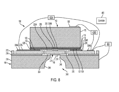
[0080] Fig. 8 shows another embodiment of the MEMS tunable VCSEL 100 in
cross-
section along A-A that has an outer proximal-side electrostatic cavity 226A
and an inner
proximal-side electrostatic cavity 226B with respect to the center optical
axis. In this
embodiment, a metal contact 130 is added to the backside of the VCSEL spacer
115.
[0081] An outer proximal-side electrostatic cavity driver 426A is connected
as
described previously to apply a voltage between the membrane layer 212 via the
membrane
wire bond pad 334B and the VCSEL proximal-side electrostatic cavity electrode
metal 122
via the left VCSEL electrode wire bond pad 334A. In this way, the controller
400 controls
an outer proximal-side electrostatic cavity 226A by controlling the outer
proximal-side
electrostatic cavity driver 426A to establish an electrical potential or
voltage to
electrostatically translate the membrane structure 214 of the membrane layer
212 toward
the VCSEL device 112.
[0082] The controller 400 however also controls an inner proximal-side
electrostatic
cavity 226B by controlling inner proximal-side electrostatic driver 426B to
generate an
13
CA 03226894 2024-01-18
WO 2023/022910 PCT/US2022/039911
electrostatic force to further translate the membrane structure 214 of the
membrane layer
212 toward the VCSEL device 112. Specifically, the inner proximal-side
electrostatic
cavity driver 426B is connected to both the membrane wire bond pad 334B and
the metal
VCSEL spacer contact 130 to apply an electrical potential or voltage between
the VCSEL
device 112 and membrane layer 212 under the control of the controller 400.
This increases
the pull-in force by effectively increasing the area of the electrostatic
cavity on the
proximal side. In addition, the gap in the inner proximal-side electrostatic
cavity is often
smaller in absolute terms in the direction of the optical axis, and tends to
have higher
dimensional precision in terms of manufacturing variability. Moreover, the
presence of the
membrane mirror 250 increases the electric field strength, the electrical
permittivity of the
mirror effectively reduces the gap.
[0083] In one mode of operation, one of the drivers: the outer proximal-
side
electrostatic cavity driver 426A or the inner proximal-side electrostatic
driver 426B, is
used to pull the membrane structure to an initial position associated with a
desired start
emission wavelength of the VCSEL 100, then the other of the two drivers 426A,
426B is
used by the controller to sweep the emission wavelength through a desired
spectral scan
band.
[0084] Fig. 9 shows another embodiment of the MEMS tunable VCSEL 100 in
cross-
section along A-A that has an outer proximal-side electrostatic cavity 226A
and an inner
proximal-side electrostatic cavity 226B. In this embodiment, the metal contact
130 is again
added to the backside of the VCSEL spacer 115.
[0085] The outer proximal-side electrostatic cavity driver 426A is
connected to apply a
voltage between the membrane layer 212 via the membrane wire bond pad 334B and
the
VCSEL proximal-side electrostatic cavity electrode metal 122 via the left
VCSEL
electrode wire bond pad 334A. In this way, the controller 400 controls the
outer proximal-
side electrostatic cavity 226A by controlling the outer proximal-side
electrostatic cavity
driver 426A to translate the membrane structure 214 of the membrane layer 212
toward the
VCSEL device 112.
[0086] The controller 400 however also controls the inner proximal-side
electrostatic
cavity 226B by controlling the inner proximal-side electrostatic driver 426B
to further
translate the membrane structure 214 of the membrane layer 212 toward the
VCSEL device
112. In this example, the inner proximal-side electrostatic cavity driver 426B
is connected
14
CA 03226894 2024-01-18
WO 2023/022910 PCT/US2022/039911
to both the VCSEL proximal-side electrostatic cavity electrode metal 122 via
the left
VCSEL electrode wire bond pad 334A and the metal VCSEL spacer contact 130 to
apply a
separately controlled voltage between the VCSEL device 112 and membrane layer
212,
again increasing the pull-in force by effectively increasing the area of the
electrostatic
cavity on the proximal side.
[0087] In this embodiment, the distal-side electrostatic cavity driver 424
can also be
used to apply a voltage between the handle wafer material 210 via the handle
wire bond
pad 334C and the membrane layer 212 via the membrane wire bond pad 334B to
additionally pull the membrane structure 214 toward the handle wafer 210.
[0088] Fig. 10 shows another embodiment of the MEMS tunable VCSEL 100 in
cross-
section along A-A that is configured to avoid charging of the dielectric
layers of the mirror
250.
[0089] Here a proximal-side electrostatic cavity driver 426 applies a
voltage between
the VCSEL proximal-side electrostatic cavity electrode metal 122 via the left
VCSEL
electrode wire bond pad 334A and both the metal contact 130 of the VCSEL
spacer 115
and the membrane wire bond pad 334B. This way, the VCSEL 112 and the membrane
layer 212 are at the same potential during operation and the inner proximal-
side
electrostatic cavity 226B is basically deactivated as a driving modality.
Thus, only the
outer proximal-side electrostatic cavity 226A is used to deflect the membrane
structure 214
toward the VCSEL. The distal-side electrostatic cavity driver 424 is used to
apply a
voltage between the handle wafer material 210 via the handle wire bond pad
334C and the
membrane layer 212 via the membrane wire bond pad 334B to additionally pull
the
membrane structure 214 toward the handle wafer 210 under the operation of the
controller
400.
[0090] Fig. 11 also shows an example of an optically pumped tunable VCSEL
swept
source system 101 employing the VCSEL 100, which system has been integrated
into a
single module.
[0091] Light from a pump chip 760 is coupled to a bench 740 via a pump
optical fiber
742. The pump light 712 from the optical fiber 742 is collimated by a first
lens LensA that
is affixed to the bench 740. The pump light 712 then is transmitted through
the dichroic
mirror 732 and then focused by a second lens LensB onto the half VCSEL 112 of
the
VCSEL 100.
CA 03226894 2024-01-18
WO 2023/022910 PCT/US2022/039911
[0092] Preferably, the bench 740, in turn, is installed in a hermetic
package 744 with
optical fibers passing through fiber-feedthroughs 746, 748 of the package 744.
[0093] The dichroic mirror 732 is reflective to longer wavelength of the
VCSEL light
734, emitted by the VCSEL 100, but transmissive to the pump light 712, 724 in
the
illustrated example. Specifically in the illustrated example, the tunable
signal from the
VCSEL 100 is reflected by the dichroic mirror 732, which is affixed to the
bench 740, and
directed to a fold mirror 750 which is also affixed to the bench 740 and then
to a third lens
752, which is affixed to the bench 740. The third lens 752 focuses light into
an entrance
aperture of an output optical fiber 754.
[0094] More details of this specific design can be found in U.S. Pat. Appl.
Pub. No.
US 2019/0348813 Al, which is incorporated herein by this reference in its
entirety.
[0095] During operation, the controller 400 energizes the pump 760 to
optically pump
active region 118 of the VCSEL device 112. At the same time, the controller
400 controls
the proximal-side electrostatic cavity 226 and controller 400 controls the
distal-side
electrostatic cavity 224 by controlling distal side electrostatic driver 424.
[0096] While this invention has been particularly shown and described with
references
to preferred embodiments thereof, it will be understood by those skilled in
the art that
various changes in form and details may be made therein without departing from
the scope
of the invention encompassed by the appended claims.
16