Note: Descriptions are shown in the official language in which they were submitted.
CA 03227543 2024-01-25
WO 2023/009652 PCT/US2022/038561
SYSTEMS AND METHODS FOR CONTROL OF NONISOLATED BIDIRECTIONAL POWER
CONVERTERS
CROSS-REFERENCE TO RELATED APPLICATIONS
[0001] This application claims priority to U.S. Provisional Application
No.
63/226,136, filed on July 27, 2021, U.S. Provisional Application No.
63/242,840, filed on
September 10, 2021, U.S. Provisional Application No. 63/345,896, filed May 25,
2022, U.S.
Provisional Application No. 63/351,768, filed on June 13, 2022, U.S.
Provisional Application
No. 63/226,059, filed July 27, 2021, U.S. Provisional Application No.
63/270,311, filed
October 21, 2021, and U.S. Provisional Application No. 63/319,122, filed March
11, 2022,
each of which is hereby incorporated by reference in its entirety.
STATEMENT REGARDING FEDERALLY SPONSORED RESEARCH
[0002] This invention was made with government support under 1653574
awarded
by the National Science Foundation. The government has certain rights in the
invention.
BACKGROUND
[0003] Power converters of various types have been produced and used in
many
industries and contexts. Example power converters include alternating current
(AC) to
direct current (DC) rectifiers, DC to AC inverters, and DC to DC converters.
AC to DC rectifiers,
also referred to as AC/DC rectifiers, converter AC power to DC power. DC to AC
inverters,
also referred to as DC/AC inverters, convert DC power to AC power. Power
converters can
-1-
CA 03227543 2024-01-25
WO 2023/009652 PCT/US2022/038561
be used for various purposes, such as rectifying AC power from an AC grid
power source to
DC power for charging a battery, or inverting DC power from a battery to AC
power to drive
a motor or supply AC power to an AC grid. Further, power converters can be
used in various
contexts, such as in or connected to an electric vehicle, an engine generator,
solar panels, and
the like.
SUMMARY
[0004] Power converters may be described in terms of power conversion
efficiency,
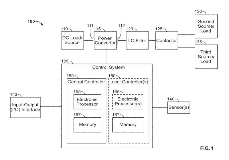
power density, and cost, among other characteristics. Generally, it is
desirable to have power
converters with higher power efficiency, higher power density, and lower cost.
A highly
efficient power converter is able to convert power (e.g., AC to DC, DC to AC,
and/or DC to DC)
without significant losses in energy. A low efficiency power converter
experiences higher
losses in energy during the power conversion. Such energy losses may manifest
as heat
generated by the power converter while converting power, for example. Power
efficiency for
a power converter, inductor, or other electronic component may be expressed as
a
percentage between 0 and 100% and determined based on the power input to the
component and the power output from the component using the
equation: Power Efficiency = Power Out. A power converter with high power
density has a
Power In
high ratio of power output by the power converter compared to the physical
space occupied
by the power converter. The power density can be calculated using the
equation:
Power Out
Power Density = .
Volume of Power Converter
-2-
CA 03227543 2024-01-25
WO 2023/009652 PCT/US2022/038561
[0005] Energy costs, including monetary costs and environmental costs,
continue to
be an important factor across many industries that incorporate power
converters.
Accordingly, even slight increases (e.g., of tenths of a percent) in power
efficiency for a power
converter can be significant and highly desirable. Similarly, reductions in
materials and size
of power converters can be significant and highly desirable, allowing
reductions in costs and
physical space to accommodate power converters in systems that incorporate
power
converters.
[0006] In grid-connected power converter applications, such as electric
vehicle (EV)
chargers and photovoltaic (PV) power supplies, leakage current and DC bus
utilization are
factors that influence the performance. For the leakage current issue, a bulky
line frequency
transformer is typically installed to block the leakage path at the point of
common coupling
(PCC) which increases the cost, volume, and weight of the system. For the DC
bus utilization,
the DC bus voltage needs to be stepped up to be at least twice of the grid
voltage amplitude
to avoid saturation issue which brings extra switching losses and challenges
to the switch
voltage tolerance capability.
[0007] Bidirectional power converters may be used to both charge a DC
source using
AC power and drive AC motors using DC power from the DC source. Such power
converters,
when included in an electric vehicle, may also be referred to as an integrated
charger. An
integrated charger may both be used as a primary charging interface for a
battery of the
electric vehicle, and also as the traction inverter to drive a motor of the
electric vehicle. By
using a dual-purpose power converter, rather than separate charger converter
and traction
inverter, material costs and size may be reduced. However, relative to
dedicated power
converters, dual-purpose power converters add complexities in designing an
efficient and
-3-
CA 03227543 2024-01-25
WO 2023/009652 PCT/US2022/038561
effective converter for both charging and traction modes. Further, the design
factors extend
beyond efficiency concerns because, without proper design, power converters
can reduce
motor lifetime due to leakage currents and/or common mode voltages causing
current
spikes in one or more of the motor bearings, motor shaft, motor windings, and
gear train that
can damage and reduce the lifetime of these components, respectively.
[0008] Some embodiments disclosed herein address these or other issues.
For
example, some embodiments disclosed herein are directed to non-isolated power
converters
with one or more of (i) injection of a multiple of an N-th phase harmonic for
zero sequence
voltage control, (ii) a cascaded control system, (iii) model predictive
control (MPC) for active
damping to mitigate resonance, (iv) variable frequency critical soft switching
(VFCSS), and
(v) modular converter blocks. These features may be included in embodiments of
a power
converter independently or in any combination. For example, a power converter
may include
one of the above-noted features, any two of the above-noted features, any
three of the above-
noted features, any four of the above-noted features, or all five of the above-
noted features.
Additionally, in combination with any of these embodiments, the power
converter may
include at least one LC filter for each of the N phases of the power converter
(where N 1),
where a capacitor of each LC filter is connected to a DC bus positive or
negative terminal of
the power converter and, in some cases, a further a capacitor of each LC
filter is connected
to the other of the DC bus positive or negative terminal of the power
converter. These
capacitors of multiple phases having a common point connected to the DC bus
positive or
negative terminals create a bypassing path for zero sequence voltage control.
The capacitor
coupled to the DC bus positive terminal (an upper capacitor) may also reduce
both EMI and
the total ripple current handling requirements of the power converter without
increasing
-4-
CA 03227543 2024-01-25
WO 2023/009652 PCT/US2022/038561
the total capacitance or volume. In some embodiments disclosed herein, an
additional drain-
source capacitor (CDs) is coupled across the drain and source terminals of the
power
switching elements, which can slow a voltage rise during an ON-to-OFF
transition. This
slowed voltage rise can, in turn, reduce the switching losses of the power
switching elements.
[0009] Some embodiments disclosed herein include systems, methods, and
other
implementations (including hardware, software, and hybrid hardware/software
implementations) directed to a modular model predictive control (MPC) method
for a novel
non-isolated N-phase DC/AC, for N 1, converter with the capabilities of zero
sequence
voltage stabilization and, optionally, regulated common mode voltage injection
(e.g., a third
harmonic injection (THI) for a three-phase system, or any other multiple of
harmonic) for
the purpose of increasing the available fundamental frequency AC voltage
magnitude for a
given DC voltage. When N=1 or N=2, the DC/AC power converter is considered to
be a single-
phase system. When N=3, the power converter is a three-phase system, and when
N> 3, the
power converter is referred to as a multiphase system. Although the
description herein may
focus on 3-phase system, the various implementations and features described
are applicable
to any number of phases.
[0010] This non-isolated topology is designed to connect the common point
of three-
phase LC filter capacitors and positive/negative DC bus terminals to bypass
the zero-
sequence leakage current. A zero-sequence voltage MPC controller stabilizes
the zero-
sequence capacitor voltage to be, in some embodiments, a constant of
approximately half DC
bus voltage. Thus, the leakage current flowing through the grid or other
coupled elements is
attenuated. Further, the regulated third harmonic voltage injection (THI)
techniques
disclosed herein improve the DC bus utilization. By adding the third harmonic
to the zero-
-5-
CA 03227543 2024-01-25
WO 2023/009652 PCT/US2022/038561
sequence voltage MPC reference, the stability and robustness are improved.
Compared to
traditional THI techniques, the grid connection power quality is improved
because no extra
harmonics are injected to the grid. Per-phase, explicit MPC simplifies the
execution
complexity on a controller (e.g., a digital signal processor (DSP)) and does
not need to update
the angular speed in the state space matrix, which allows for the MPC
optimization offline.
Compared with a traditional proportional integral (PI) controller, embodiments
of the MPC
controller disclosed herein provides power converter control with improved
dynamic
performance and control bandwidth with faster response.
[0011] The effective zero-sequence voltage control (through the LC
filters and control
schemes disclosed herein) also serves to reduce certain bearing currents,
shaft currents,
motor winding currents, gear train currents, and other currents that can
potentially damage
and reduce the life of motors and their components (bearings, shafts, wiring,
etc.). For
example, currents caused by high rates of change of voltage (dV/dt),
especially at higher
voltages (e.g., above 400 V, above or approaching 800 V, and levels between)
can cause
damage to motor bearings, motor shafts, motor windings (e.g., insulation may
be damaged),
and gear trains (e.g., bearing currents can propagate into the gear train via
electromagnetic
interference (EMI) or noise, vibration, harshness (NVH) resulting from the
damaged bearing
race walls).
[0012] In some examples, the power converter is driven using a variable
frequency
critical soft switching (VFCSS) scheme. The VFCSS scheme can provide improved
efficiency
and reduced filter volume (i.e., improved power density) for the power
converter.
-6-
CA 03227543 2024-01-25
WO 2023/009652 PCT/US2022/038561
[0013] In some examples, the power converter is implemented through a
combination of modular converter units or modules, also referred to as
autoconverter
modules (ACMs) that are coupled together like building blocks to form the
power converter
having desired specifications. Each ACM may include, for example, a circuit
board having
input and output connection terminals (e.g., to couple to other ACMs and a
central
controller), as well as a converter block including power switching elements
and an LC filter
(e.g., configured in a half bridge configuration).
In one embodiment, a non-isolated power converter system is provided. The
system includes
an N-phase power converter stage having to an alternating current (AC) side
and a direct
current (DC) side, with N 1; an N-phase LC filter comprising one or more
capacitors,
wherein respective one or more neutral points of the one or more capacitors
are electrically
connected to a DC negative terminal of a DC source; and a control system
configured to drive
power switching elements of the N-phase power converter stage to convert
received power
and to output converted power, the control system configured to drive the
power switching
elements using variable frequency soft switching at a frequency of at least 20
kHz.
[0014] In one embodiment, a method for power conversion is provided. The
method
includes receiving input power, by an N-phase power converter stage, from an
alternating
current (AC) side or a direct current (DC) side, with N 1; filtering, by an N-
phase LC filter
comprising one or more capacitors, at the AC side of the N-phase power
converter stage,
wherein respective one or more neutral points of the one or more capacitors
are electrically
connected to a DC negative terminal of a DC source; and driving, by a control
system, power
switching elements of the N-phase power converter stage to convert the input
power and to
-7-
CA 03227543 2024-01-25
WO 2023/009652 PCT/US2022/038561
output converted power, the control system configured to drive the power
switching
elements using variable frequency soft switching at a frequency of at least 20
kHz.
[0015] In one embodiment, a non-isolated power converter system for an
electric
vehicle is provided. The system includes an N-phase power converter stage
having an
alternating current (AC) side and a direct current (DC) side, with N 1,
wherein the DC side
includes DC source terminals; an N-phase LCL filter comprising one or more
capacitors,
wherein respective one or more neutral points of the one or more capacitors
are electrically
connected to a negative DC terminal of the DC source terminals; and a control
system
configured to drive power switching elements of the N-phase power converter
stage to: in a
charging mode, convert input AC power received via AC terminals to output DC
power
provided to the DC source terminals to charge the DC source, and, in a
traction mode, convert
input DC power received via the DC source terminals to output AC power
provided to the AC
terminals to drive a motor.
[0016] In one embodiment, a method of converting power for an electric
vehicle is
provided. The method includes receiving, by an N-phase power converter stage,
input power
from an alternating current (AC) side having AC terminals or a direct current
(DC) side
having DC source terminals, with N 1; filtering, by an N-phase LC filter
comprising one or
more capacitors, at the AC side of the N-phase power converter stage, wherein
respective
one or more neutral points of the one or more capacitors are electrically
connected to a DC
negative terminal of the DC source terminals; and driving, by a control
system, power
switching elements of the N-phase power converter stage to: in a charging
mode, convert
input AC power received via the AC terminals to output DC power provided to
the DC source
terminals to charge a DC source, and in a traction mode, convert input DC
power received
-8-
CA 03227543 2024-01-25
WO 2023/009652 PCT/US2022/038561
via the DC source terminals to output AC power provided to the AC terminals to
drive a
motor.
[0017] The foregoing and other aspects and advantages of the present
disclosure will
appear from the following description. In the description, reference is made
to the
accompanying drawings that form a part hereof, and in which there is shown by
way of
illustration one or more embodiment. These embodiments do not necessarily
represent the
full scope of the invention, however, and reference is therefore made to the
claims and herein
for interpreting the scope of the invention. Like reference numerals will be
used to refer to
like parts from Figure to Figure in the following description.
BRIEF DESCRIPTION OF THE DRAWINGS
[0018] FIG. 1 illustrates a power converter system according to some
embodiments.
[0019] FIG. 2 illustrates a half-bridge power converter according to some
embodiments.
[0020] FIG. 3A illustrates multiphase power converter system according to
some
embodiments.
[0021] FIGS. 3B-3C illustrate a multiphase power converter in a charging
mode and a
traction mode, respectively, according to some embodiments.
[0022] FIG. 3D illustrates a simplified equivalent circuit of parasitic
capacitances of
an electric machine.
[0023] FIG. 4 illustrates a converter system according to some
embodiments.
-9-
CA 03227543 2024-01-25
WO 2023/009652 PCT/US2022/038561
[0024] FIG. SA and SB illustrate waveforms for third harmonic injection
according to
some embodiments.
[0025] FIG. 6 illustrates a communication system for a cascaded control
system
according to some embodiments.
[0026] FIG. 7 illustrates an MPC-based converter system according to some
embodiments.
[0027] FIG. 8 illustrates a model predictive control (MPC) control system
according
to some embodiments.
[0028] FIG. 9 illustrates a state estimator according to some
embodiments.
[0029] FIG. 10 illustrates a timing diagram and boundary conditions for
soft switching
according to some embodiments.
[0030] FIG. 11 illustrates a control system for variable frequency
critical soft
switching according to some embodiments.
[0031] FIG. 12 illustrates a power converter system including model
predictive
control (MPC) with variable frequency critical soft switching (VFCSS)
according to some
embodiments.
[0032] FIG. 13 illustrates a control system for local MPC-VFCSS control
using variable-
continuous-frequency critical-soft-switching (VCFCCS) according to some
embodiments.
[0033] FIG. 14 illustrates a control system for local MPC-VFCSS control
using variable-
discrete-frequency critical-soft-switching (VDFCCS) according to some
embodiments.
-10-
CA 03227543 2024-01-25
WO 2023/009652 PCT/US2022/038561
[0034] FIG. 15 illustrates waveforms for VCFCCS and VDFCCS control
according to
some embodiments.
[0035] FIG. 16 illustrates a plot of carrier signals and sampling signals
for VDFCCS
control according to some embodiments.
[0036] FIGS. 17A and 17B illustrate respective plots of experimental
results of a
power converter according to some embodiments.
[0037] FIGS. 18A and 18B illustrate autoconverter modules according to
some
embodiments.
[0038] FIG. 19 illustrates a power converter incorporating autoconverter
modules
according to some embodiments.
[0039] FIG. 20 illustrates a process for converting power using variable
frequency
critical soft switching, according to some embodiments.
[0040] FIG. 21 illustrates a process for converting power in a charging
mode and a
traction mode, according to some embodiments.
[0041] FIGS. 22 and 23 illustrate respective efficiency plots of
experimental results of
a power converter according to some embodiments.
[0042] FIG. 24 illustrates a configurable power converter architecture
according to
some embodiments.
[0043] FIGS. 25A and 25B illustrate a single-phase grid application
configuration of
the power converter architecture of FIG. 24, according to some embodiments.
-11-
CA 03227543 2024-01-25
WO 2023/009652 PCT/US2022/038561
[0044] FIGS. 26A and 26B illustrate a three-phase grid application
configuration of
the power converter architecture of FIG. 24, according to some embodiments.
[0045] FIGS. 27A and 27B illustrate a motor application configuration of
the power
converter architecture of FIG. 24, according to some embodiments.
DETAILED DESCRIPTION
[0046] One or more embodiments are described and illustrated in the
following
description and accompanying drawings. These embodiments are not limited to
the specific
details provided herein and may be modified in various ways. Furthermore,
other
embodiments may exist that are not described herein. Also, functions performed
by multiple
components may be consolidated and performed by a single component. Similarly,
the
functions described herein as being performed by one component may be
performed by
multiple components in a distributed manner. Additionally, a component
described as
performing particular functionality may also perform additional functionality
not described
herein. For example, a device or structure that is "configured" in a certain
way is configured
in at least that way, but may also be configured in ways that are not listed.
[0047] As used in the present application, "non-transitory computer-
readable
medium" comprises all computer-readable media but does not consist of a
transitory,
propagating signal. Accordingly, non-transitory computer-readable medium may
include,
for example, a hard disk, a CD-ROM, an optical storage device, a magnetic
storage device, a
ROM (Read Only Memory), a RAM (Random Access Memory), register memory, a
processor
cache, or any combination thereof.
-12-
CA 03227543 2024-01-25
WO 2023/009652 PCT/US2022/038561
[0048] In addition, the phraseology and terminology used herein is for
the purpose of
description and should not be regarded as limiting. For example, the use of
"comprising,"
"including," "containing," "having," and variations thereof herein is meant to
encompass the
items listed thereafter and equivalents thereof as well as additional items.
Additionally, the
terms "connected" and "coupled" are used broadly and encompass both direct and
indirect
connecting and coupling, and may refer to physical or electrical connections
or couplings.
Furthermore, the phase "and/or" used with two or more items is intended to
cover the items
individually and both items together. For example, "a and/or b" is intended to
cover: a (and
not b); b (and not a); and a and b.
[0049] Disclosed herein are systems and methods related to power
converters, also
referred to as voltage converters, that can provide power conversion with
increased power
efficiency, increased power density, and/or reduced cost, among other
advantages.
[0050] FIG. 1 illustrates a power converter system 100 in accordance with
some
embodiments. The power converter system 100 includes a control system 105, a
first direct
current (DC) load/source 110, a power converter 115 (also referred to as a
power converter
stage 115), an LC filter 120, a contactor 125, a second source/load 130, a
third source/load
135, and one or more sensors 140. The control system 105 includes a central
controller 150
with an electronic processor 155 and a memory 157, and, optionally, in some
embodiments,
includes one or more local controllers 160, each having an electronic
processor 165 and a
memory 167. The power converter system 100, as well as the other power
converter systems
provided herein, may be non-isolated power converter systems. That is, the
power converter
system may be coupled to an AC source (e.g., single or three phase power grid)
or AC load
(e.g., single or 3-phase motor) without a transformer. Use of a transformer is
common in
-13-
CA 03227543 2024-01-25
WO 2023/009652 PCT/US2022/038561
electrical circuits to provide isolation between the power converter and an AC
source or load.
However, such a transformer can add inefficiencies and size or volume to the
power
converter. Accordingly, power converter systems provided herein are non-
isolated, also
referred to as transformerless, to increase efficiency and/or reduce size of
the power
converter systems. Because the power converters are provided without isolation
by a
transformer, the power converters may include additional features to prevent
transmission
of unwanted signals or current (e.g., leakage current) from passing between
the power
converters and other circuit components (e.g., DC sources, DC loads, AC
sources, AC loads,
and other structures in contact with or supporting the power converters).
[0051] In operation, generally, the control system 105 controls power
switching
elements of the power converter 115 with control signaling (e.g., pulse-width
modulated
(PWM) signals) to convert power (i) from the DC load/source 110 functioning as
a source to
the second source/load 130 or the third source/load 135 (depending on the
state of the
contactor 125) functioning as a load, or (ii) from the second source/load 130
or the third
source/load 135 (depending on the state of the contactor 125) functioning as a
source to the
DC load/source 110 functioning as a load. Accordingly, when the DC load/source
110 is
functioning as a source for the power converter 115, the second source/load
130 (or third
source/load 135, depending on the state of the contactor 125) is functioning
as a load for the
power converter 115. Conversely, when the DC load/source 110 is functioning as
a load for
the power converter 115, the second source/load 130 (or third source/load 135,
depending
on the state of the contactor 125) is functioning as a source for the power
converter 115.
[0052] The DC load/source 110 may be a direct power (DC) load, a DC
source, or both
a DC load and DC source (i.e., functioning as DC source in some instances and
as a DC load in
-14-
CA 03227543 2024-01-25
WO 2023/009652 PCT/US2022/038561
other instances, depending on the mode of the power converter 115). In some
examples, the
DC load/source 110 is a battery. In other examples, DC load/source 110 may be
a capacitor,
an ultracapacitor, a DC power supply from rectified AC source (e.g., AC grid
power converted
to DC power by diode bridge rectifier), or the like. The second source/load
130 may be an
AC load, an AC source, both an AC load and AC source (i.e., functioning as an
AC source in
some instances and as an AC load in other instances, depending on the mode of
the power
converter 115), a DC load, a DC source, both a DC load and DC source (i.e.,
functioning as a
DC source in some instances and as a DC load in other instances, depending on
the mode of
the power converter 115). In some examples, the second source/load 130 may be
an electric
(AC) motor, an AC generator, AC power supply grid, a DC battery, a DC
capacitor, a DC
ultracapacitor, a DC power supply from rectified AC source (e.g., AC grid
power converted to
DC power by diode bridge rectifier), or the like. The third source/load 135
may be an AC
load, an AC source, both an AC load and AC source (i.e., functioning as an AC
source in some
instances and as an AC load in other instances, depending on the mode of the
power
converter 115), a DC load, a DC source, both a DC load and DC source (i.e.,
functioning as a
DC source in some instances and as a DC load in other instances, depending on
the mode of
the power converter 115). In some examples, the third source/load 135 may be
an electric
(AC) motor, an AC generator, AC power supply grid, a DC battery, a DC
capacitor, a DC
ultracapacitor, a DC power supply from rectified AC source (e.g., AC grid
power converted to
DC power by diode bridge rectifier), or the like.
[0053] In some examples, the DC load/source 110 is a DC battery (e.g., an
electric
vehicle battery), the second source/load 130 is an AC grid, and the third
source/load 135 is
an AC motor (e.g., an electric vehicle motor). In this case, the power
converter 115 may
-15-
CA 03227543 2024-01-25
WO 2023/009652 PCT/US2022/038561
function as a hi-directional converter that operates in a DC/AC traction mode
(or motor
mode) to drive the third source/load 135 (motor) with AC power converted from
DC power
from the DC load/source 110 (battery), and an AC/DC charging mode to charge
the DC
load/source 110 (battery) with DC power converted from AC power from the
second
load/source 130 (AC grid). In some other examples, the DC load/source 110 is a
DC source,
the second source/load 130 is an AC motor, and no third source/load 135 is
present in the
system 100.
[0054] The contactor 125 is an electrically controlled switch, and may
be, for example,
a contactor, a relay, MOSFET, or the like. In some examples of the system 100,
the contactor
125 is not present and, instead, the LC filter 120 is connected to both the
second source/load
130 and the third source/load 135 simultaneously. However, other control
techniques are
employed to prevent, for example, driving the third source/load 135 as a load
(e.g., a motor),
when receiving power from the second source/load 130 as a source (e.g., an AC
grid).
[0055] The DC load/source 110 is coupled to the power converter 115 at a
first (DC)
side or section 111 of the power converter 115, and the second source/load 130
is coupled
to the power converter 115 at a second (AC) side or section 112 of the power
converter 115.
The first side may also be referred to as an input side or an output side of
the power
converter 115, depending on the mode of the power converter, or as a DC side
of the power
converter 115. The second side may also be referred to as an input side or an
output side of
the power converter, depending on the mode of the power converter, or as an AC
side of the
power converter 115. In some embodiments, the second side of the power
converter 115
may be an AC side having single phase AC power, three-phase AC power, or AC
power with
another number of phases.
-16-
CA 03227543 2024-01-25
WO 2023/009652 PCT/US2022/038561
[0056] In some embodiments, the power converter 115 operates with a high
DC
voltage level. For example, in operation, the DC side of the power converter
115 has a DC
voltage (e.g., across input terminals of the power converter 115) of at least
200 V, at least
600 V, at least 800 V, at least 1000 V, at least 1200 V, between 200 V and
1200 V, between
600 V and 1200 V, between 800 V and 1200 V, or another range. Such high DC
voltage levels
may be desirable in some contexts, such as some electric vehicles. For
example, some current
electric vehicles (e.g., passenger vehicles and hybrid electric vehicles)
operate with a DC bus
voltage of between about 200 V and 400 V. This DC bus voltage for passenger
electric vehicle
may increase in the future. Further, some current electric vehicles (e.g.,
class 4-8, off-road,
or otherwise larger electric vehicles) can operate with a DC bus voltage of
more than 1000
V. However, high DC voltage levels may introduce challenges into a typical
power converter
system, such as an increase in leakage currents, increases in common mode
voltage, higher
rates of change in common mode voltage, and the like. These challenges can
lead to
resonance on the LC filter 120, shaft voltages, excessive bearing currents
(e.g., from
discharge events when lubricant dielectric breakdown occurs) that can result
in bearing
failures, excessive motor shaft currents, excessive motor winding currents
(e.g., insulation
may be damaged), and excessive gear train currents (e.g., bearing currents can
propagate
into the gear train via electromagnetic interference (EMI) or noise,
vibration, harshness
(NVH) resulting from the damaged bearing race walls). Embodiments described
herein,
however, can mitigate such challenges through improved LC filters and through
control
techniques including control techniques that use harmonic injection, cascaded
controllers,
MPC control, and/or variable frequency critical soft switching (VFCSS).
-17-
CA 03227543 2024-01-25
WO 2023/009652 PCT/US2022/038561
[0057] The LC filter 120, which may be referred to as an N-phase LC
filter, includes an
LC filter for each phase of the power converter 115. Each LC filter of the N-
phase LC filter
may include at least an inductor and a capacitor, or at least an inductor and
two capacitors,
as described in further detail below (see, e.g., discussion of FIGS. 2 and 3).
[0058] The sensor(s) 140 include, for example, one or more current
sensors and/or
one or more a voltage sensors. For example, the sensor(s) 140 may include a
respective
current sensor and/or voltage sensor to monitor a current and/or voltage of
one or more of
the DC load source 110, each phase of the second source/load 130, each phase
of the third
source/load 135, each phase of the LC filter 120, or other nodes or components
of the power
converter 115. For example, when the LC filter 120 is a three-phase LC filter,
the sensors 140
may include at least three current sensors, one for sensing current at each
phase of a three
phase LC filter 120. In some embodiments, additional or fewer sensors 140 are
included in
the system 100. For example, the sensors 140 may also include one or more
vibration
sensors, temperature sensors, and the like. In some examples, the control
system 105 infers
a characteristic (e.g., current or voltage) of the power converter 115, rather
than directly
sensing the characteristic. The sensor(s) 140 may provide sensor data to the
control system
105 indicative of the sensed characteristics of the system 100. Such sensor
data may,
accordingly, indicate electrical operational characteristics of the system
100. In some
examples, the control system 105 infers or estimates a characteristic (e.g.,
current or voltage)
at one or more nodes of the power converter 115 based on the sensor data of a
sensor 140
that senses a different type of characteristic or even a different component,
rather than
directly sensing the characteristic. Further description of such inferencing
or estimating are
provided below with respect to state estimation.
-18-
CA 03227543 2024-01-25
WO 2023/009652 PCT/US2022/038561
[0059] The input-output (I/O) interface 142 includes or is configured to
receive input
from one or more inputs (e.g., one or more buttons, switches, touch screen,
keyboard, and
the like), and/or includes or is configured to provide output to one or more
outputs (e.g.,
LEDs, display screen, speakers, tactile generator, and the like). Other
electronic devices
and/or users may communicate with the system 100 and, in particular, the
control system
105, via the I/O interface 142. For example, the control system 105 may
receive commands
(e.g., from a user or another device) for the power converter system 100
indicating a target
torque, target speed, target power level, conversion type, or the like. The
control system 105,
in response, may drive the power converter 115 to achieve the target and/or
conversion
type indicated by the command.
[0060] The control system 105 generally monitors the system 100 including
the
power converter 115 (e.g., based on sensor data from the sensor(s) 140),
receives commands
(e.g., via the input/output interface 142), and controls the power switching
elements of the
power converter 115 with control signaling (e.g., pulse-width modulated (PWM)
signals) to
convert power (e.g., in accordance with the sensor data and/or the commands).
In some
embodiments, the control system 105 includes a controller (e.g., the central
controller 150)
that performs this monitoring and control without additional local
controllers. In other
embodiments, the control system 105 is a cascaded control system including a
central
controller 150 and one or more local controllers 160. The cascaded control
system may
communicate in real time (e.g., each control cycle) monitoring information
(e.g., sensor data)
and control information between the central controller 150 and the one or more
local
controller 160. In some examples, the local controller(s) 160 each implement
model
predictive control (MPC) or another regulation control scheme (e.g., PID
control, PI control,
-19-
CA 03227543 2024-01-25
WO 2023/009652 PCT/US2022/038561
or the like). In some examples, the central controller implements a non-MPC
regulation
technique, such as proportional integral derivative (PID) control or
proportional integral
(PI) control.
[0061] Each controller of the control system 105, including the central
controller 150
and the local controllers 160, is an electronic controller that may include an
electronic
processor. Such an electronic controller may further include a memory (e.g.,
the memory 157
or 167). The memory is, for example, one or more of a read only memory (ROM),
random
access memory (RAM), or other non-transitory computer-readable media. The
electronic
processor 155, 165 is configured to, among other things, receive instructions
and data from
the memory 157, 167 and execute the instructions to, for example, carry out
the functionality
of the associated controller described herein, including the processes
described herein. For
example, the memory may include control software. In some embodiments, instead
of or in
addition to executing software from the memory to carry out the functionality
of the
controller described herein, the electronic processor includes one or more
hardware circuit
elements configured to perform some or all of this functionality.
Additionally, although a
particular controller, electronic processor, and memory may be referred to as
a respective,
single unit herein, in some embodiments, one or more of these components is a
distributed
component. For example, in some embodiments, an electronic processor includes
one or
more microprocessors and/or hardware circuit elements.
[0062] FIG. 2 illustrates an example of a half-bridge converter 200 that
may serve as
the power converter 115 of the system 100 of FIG. 1. As illustrated, the
converter 200
includes DC terminals 220 (also referred to as DC nodes, DC links, DC rails,
etc.) having a
positive DC terminal 222 and a negative DC terminal 224. The converter 200
further includes
-20-
CA 03227543 2024-01-25
WO 2023/009652 PCT/US2022/038561
interface terminals 225 (also referred to as interface nodes) having a
positive interface
terminal 227 and negative interface terminal 229. The converter 200 may be
operated as a
bidirectional converter or as a unidirectional converter (in either
direction), depending on
the configuration and control of the system in which it is implemented.
Accordingly, the DC
terminals 220 may be input terminals and the interface terminals 225 may be
output
terminals in some examples (e.g., DC/DC conversion and DC/AC inversion), and
the DC
terminals 220 may be output terminals and the interface terminals 225 may be
input
terminals in some examples (e.g., AC/DC rectification). Additionally, the
interface terminals
225 may be AC input terminals (e.g., for AC/DC rectification), may be AC
output terminals
(e.g., for a DC/AC inverter), or may be DC output terminals (e.g., for DC/DC
conversion).
[0063] The converter 200 further includes a DC link capacitor (Cpc) 230,
a, a high side
(upper) power switching element (M1) 235 (also referred to as upper switch or
upper FET
235), a low side (lower) power switching element (M2) 240 (also referred to as
lower switch
or lower FET 240), a midpoint node 242 connecting a drain terminal of upper
switch 235
and a source terminal of lower switch 240, and an LC filter 245. The LC filter
245 is an
example of the LC filter 120 of the system 100 of FIG. 1 (e.g., where the LC
filter 120 is an N-
phase LC filter with N = 1).
[0064] The power switching elements 235 and 240 may be field effect
transistors
(FETs), each having a respective gate, source, and drain terminal. The FETs
may be, for
example, a MOSFET, a silicon carbide (SiC) FET, a gallium nitride (GaN) FET,
among other
types of FETs.
-21-
CA 03227543 2024-01-25
WO 2023/009652 PCT/US2022/038561
[0065] The LC filter 245 includes a switch-side inductor Lsw 250, a lower
capacitor CB
255, and an upper capacitor CA 215. The switch-side inductor Lsw 250 is
coupled between
the midpoint node 242 and a filter node 260. For example, a first end of the
switch-side
inductor Lsw 250 is coupled to the midpoint node 242, and a second end is
coupled to the
filter node 260. The lower capacitor CB 255 is coupled between the filter node
206 and the
negative DC terminal 224. For example, a first end of the lower capacitor CB
255 is coupled
to the filter node 260, and a second end is coupled to the negative DC
terminal 224. The upper
capacitor CA 215 is coupled between the filter node 260 and the positive DC
terminal 222.
For example, a first end of the lower capacitor CA 215 is coupled to the
filter node 260, and a
second end is coupled to the positive DC terminal 222.
[0066] In some examples, the LC filter 245 is an LCL filter (an LC filter
with an
additional inductor (L)), in which an additional (interface) inductor is
coupled between the
filter node 260 and the positive interface terminal 227.
[0067] The upper capacitor 215 allows for the ripple currents at both
input nodes and
output nodes (nodes 222, 227) of the converter 200 to be shared. Because the
ripple currents
on the input nodes and the ripple currents on the output nodes have some
correlation,
differential mode currents of these input and output nodes can be canceled
through this
capacitance. This reduction in differential mode current can result in
improved EMI
performance and decreased total capacitor ripple current when compared with a
typical
half-bridge converter (e.g., when the total capacitance between the two
converters is held
constant). Furthermore, the reduction in total capacitor ripple current can
allow for a
decrease in capacitor size, for example, when capacitor ripple current drives
capacitor sizing.
-22-
CA 03227543 2024-01-25
WO 2023/009652 PCT/US2022/038561
[0068] The converter further includes drain-source capacitors CDs 265a
and 265b,
each respectively coupled across one of the switches 235, 240. In particular,
a first drain-
source capacitor 265a is provided across a source terminal 270a and drain
terminal 275a of
the upper switch (M1) 235, and a second drain-source capacitor 265b is
provided across a
source terminal 270b and drain terminal 275b of the lower switch (M2) 240. The
drain-
source capacitors (CDs) 265a-b may be generically and collectively referred to
herein as
drain-source capacitor(s) (CDs) 265.
[0069] The drain-source capacitors (CDs) 265 can slow a voltage rise
during an ON-to-
OFF transition of the switches 235 and 240. This slowed voltage rise can, in
turn, reduce the
switching losses of the switches 235 and 240.
[0070] In some examples of the converter 200, one or both of the upper
capacitor CA
215 and the drain-source capacitors CDs are not included in the converter 200.
[0071] As noted, in some examples, the power converter 200 may serve as
the power
converter 115 of the system 100 in FIG. 1. In the context of the power
converter 115 (and,
thus, the power converter 200) implementing an AC/DC rectifier or a DC/AC
inverter, the
power converter 200 is a single-phase power converter 200. In some examples,
multiple
instances of the power converter 200 are paralleled to collectively serve as
the power
converter 115 of FIG. 1 and provide the single-phase conversion (whether
rectification or
inversion) or to provide a DC/DC power conversion. In some examples, the power
converter
115 is a multiphase power converter (e.g., operating with three or more phases
of AC power).
In such examples, the power converter 115 may include multiple instances of
the power
converter 200, each instance associated with a phase of the AC power, each
instance having
-23-
CA 03227543 2024-01-25
WO 2023/009652 PCT/US2022/038561
shared DC terminals 220, and each instance having independent Vinterface nodes
225.
Examples of such a power converter are provided in FIGS. 3, 4, 7, and 12. In
some of these
examples, as shown in FIGS. 19-20, multiple instances of the power converter
200 are
paralleled to collectively provide the power conversion for a respective phase
(e.g., two
parallel power converters 200 for phase A, two parallel power converters 200
for phase B,
and two parallel power converters 200 for phase C). In some examples, the
particular
number of parallel power converter 200 and the number of phases varies.
[0072] As used herein, a converter block may refer to a half bridge
circuit such as
described with respect to the converter 200 of FIG. 2. For example, a
converter block 262
may include the power switching elements 235 and 240, the LC filter 245
(including upper
capacitor 215, if present, and additional interface inductor, if present), the
interconnecting
nodes thereof (e.g., midpoint node 242, filter node 260, DC terminals 220, and
interface
terminals 225), and (if present) drain-source capacitors 265.
[0073] FIG. 3A illustrates a multiphase power converter system 300
selectively
coupled to an AC grid 302 or an AC motor 303 by the contactor 125. The
multiphase
converter system 300 includes a multiphase converter 304 coupled to a DC
source 306,
illustrated as a battery 306, on a DC side and coupled to the contactor 125
(and, thus, the
AC grid 302 or the AC motor 303) via LC filters 308. The multiphase converter
304 may
serve as the power converter 115 of the system 100 in FIG. 1.The LC filters
308, collectively
an three-phase LC filter, may serve as the LC filter 120 of the system 100 of
FIG. 1. With
reference to FIG. 1, the battery 306 is an example of the DC load/source 110;
the AC grid
302 is an example of the second source/load 130; and the AC motor 303 is an
example of
the third source/load 135. Returning to FIG. 3A, in operation, the converter
system 300
-24-
CA 03227543 2024-01-25
WO 2023/009652 PCT/US2022/038561
may function as a DC/AC inverter or an AC/DC rectifier, depending on the
sources and
switching of the power switching elements.
[0074] The AC motor 303 may be, for example, a permanent magnet rotor
synchronous machine, a wound field synchronous machine (WFSM), or another
motor. The
AC motor 303 may include a stator and rotor. The stator may include a
plurality of stator
windings that may be driven with current to generate a changing magnetic field
to cause the
rotor to rotate. The rotor may include permanent magnets, wound field, or a
combination
(hybrid) of permanent magnets and wound fields. The rotor may be coupled to a
motor draft
such that, when the rotor is rotatably driven, the motor shaft is rotatably
driven (i.e.,
rotated). The motor windings of the stator and/or rotor may have insulation,
which, as noted
above, can be damaged due to excessive currents resulting from high rates of
change of
voltage (dV/dt). The motor shaft may be supported by one or more motor
bearings to enable
the support and rotation of the shaft. For example, the motor shaft may
include a first motor
bearing at a driven end of the shaft (an end of the shaft coupled to the
rotor) and a second
motor bearing at a distal end of the shaft. In some examples, other motor
bearing
arrangements are used. The motor shaft may be further coupled to a
transmission or gearing
(a gear train) that drives an end load. For example, in the case of an
electric vehicle, the
transmission may ultimately be coupled to one or more wheels to cause the
vehicle to be
propelled. In other examples, the motor is part of an industrial equipment and
causes
rotation of another load (e.g., cutting instruments, grinders, conveyer
motors, etc.).
[0075] The multiphase converter 304, also referred to as a power
converter stage,
includes three instances of the power converter 200 (or converter block 262)
of FIG. 2, one
for each phase of the AC grid 302. Each instance includes an upper and a lower
switch 235
-25-
CA 03227543 2024-01-25
WO 2023/009652 PCT/US2022/038561
and 240. Although not illustrated, each switch 235 and 240 may include a
respective drain-
source capacitor coupled thereacross, as shown in FIG. 2. The multiphase
converter 304 is
further coupled, via the DC terminals 220, to the battery 306, and via
interface terminals
225a,b to the AC grid 302 and AC motor 303. More particularly, the interface
terminals
225a,b include three grid connection points 225a (one for each phase of the
grid) for
connecting to the AC grid 302 and three motor connection points 225b (one for
each phase
of the motor) for connecting to the AC motor 303. The multiphase converter
system 300
includes three LC filters 308. Each LC filter 308 includes components similar
to the LC filter
245 of FIG. 2. That is, each LCL filter 308 includes a switch-side inductor
250 (also labeled
Lfs,a, Lfs,b, or Lfs,c), a lower capacitor 255 (also labeled Cf,a, Cf,b, and
Cf,c), an upper capacitor 215
(also labeled Cf,a, Cf,b, or Cf,c). A neutral point 311a of the lower
capacitors 255 is coupled to
the negative DC terminal 224, such that the neutral point 311 and the negative
DC terminal
224 are a common node. Similarly, a neutral point 311b of the upper capacitors
215 is
coupled to the positive DC terminal 222. The switch-side inductor 250 is
coupled between
the midpoint node 242 and the filter node 260. The LC filters 308 are coupled
to the AC
interface terminals 225a,b via a common mode inductor (Lcm) 312. More
particularly, the
common mode inductor 312 is coupled between the filter node 260 and the
interface
terminals 225a,b. The common mode inductor 312 may assist in filtering out
leakage
currents in the system.
[0076] In the illustrated example, the multiphase converter system 300 is
coupled to
the battery 306 and the AC grid 302. In other examples, the multiphase
converter system
300 is coupled to a DC source/load other than the battery 306 (e.g., a
capacitor,
ultracapacitor, DC power supply from rectified AC power, etc.), coupled to a
different AC
-26-
CA 03227543 2024-01-25
WO 2023/009652 PCT/US2022/038561
source/load other than the grid 302 and motor 303, and/or coupled to only one
of the AC
grid 302 or the AC motor 303. Additionally, although the multiphase converter
system 300
includes the upper capacitor 215 for each phase, in some examples, the upper
capacitors 215
are not included.
[0077] As illustrated in FIG. 2 and FIG. 3A, in some examples of the
power converter
systems provided herein, the LC filter 120 (implemented as LC filter 245 in
FIG. 2 and 308 in
FIG. 3A) includes an LC filter for each phase, where a common point of each
capacitor is
connected to the DC bus negative terminal (and/or positive terminal). This
connection
creates a bypassing path for zero-sequence voltage control. By leveraging the
topological
modification and zero voltage control, the common mode voltage can be
stabilized to reduce
leakage current.
[0078] As previously noted, in some examples, the contactor 125 is not
present and,
rather, the interface terminals 225a and 225b are coupled to both the AC grid
302 and the
AC motor 303 simultaneously. In some examples, a torque cancellation scheme
may be used
such that, when AC power is received from the AC grid 302 via the interface
terminals 225a
(i.e., to be converted by the converter 304 to charge the battery 306), the
received AC power
does not cause the AC motor 303 to be driven. That is, power signals on the
terminals 225b
that may otherwise cause motor torque in the AC motor 303 are effectively
cancelled through
appropriate control of the power switching elements 235 and 240 of the
converter 304. The
implemented torque cancellation schemes may be generally known in the art.
[0079] FIGS. 3B and 3C illustrate circuit diagrams for the converter
system 300 when
incorporated into an electric vehicle (EV), represented by the EV chassis 350.
The circuit
-27-
CA 03227543 2024-01-25
WO 2023/009652 PCT/US2022/038561
diagrams illustrate the converter system 300 in two different operational
modes: a charging
mode in FIG. 3B and a traction mode in FIG. 3C. In the charging mode of FIG.
3B, the converter
304 converts received AC power from the grid 302 to DC power for charging the
battery 306.
In this mode, the contactor 125 (shown in FIG. 3A) may be configured or
controlled to
connect the AC terminals 225 to the AC grid 302, and to disconnect from the AC
motor 303.
Accordingly, the AC motor 303 is not illustrated in the diagram of FIG. 3B
(although it is
physically still present in the electric vehicle). A grid inductance between
the common mode
inductor (LCM) and the AC grid 302 is represented by grid inductors 352. A
capacitance
between the DC source 306 or the DC terminals 220 and the EV chassis 350 is
represented
by the capacitors 354.
[0080] In the traction mode of FIG. 3C, the converter 304 converts
received ADCC
power from the battery 306 to AC power to drive the AC motor 303, represented
in the
diagram as a three-phase inductor. In this mode, the contactor 125 (shown in
FIG. 3A) may
be configured or controlled to connect the AC terminals 225 to the AC motor
303, and to
disconnect from the AC grid 302. Accordingly, the AC grid 302 is not
illustrated in the
diagram of FIG. 3C, although the grid connection points 225a are still present
in the vehicle
to be able to connect to the AC grid 302. A further capacitance between the AC
motor 303
and the EV chassis 350 is represented by the capacitors 356.
[0081] In some examples, the system 300 (as well as other power converter
systems
described herein) provides a transformerless vehicle to grid (V2G) or vehicle
to everything
(V2X) interface. The systems disclosed herein, including the system 300, may
be particularly
well-suited for such operation in view of the common mode control (described
further
below) and the filtering hardware (e.g., LC filter 308) used in these systems.
In some
-28-
CA 03227543 2024-01-25
WO 2023/009652 PCT/US2022/038561
examples, the system 300 is included as part of an integrated drivetrain
solution (e.g.,
providing both a traction mode and a charging mode). In other examples, the
system 300 is
a dedicated on-board charger (e.g., having a charging mode, but not a traction
mode) or
dedicated traction drive (e.g., having a traction mode, but not a charging
mode).
[0082]
Generally, the system 300 may provide single phase AC, two phase AC, three
phase AC, or DC operation. In a V2X interface implementation, the system 300
may interact
with the grid 302 to return power or balance the grid 302, interface with
photovoltaic and
energy storage systems, and/or form a local micro-grid or the like. The
control of this V2X
interface can be done similar to one or more of the control techniques
described below
including using (1) global control at the functional level, (2) local control
at the device level,
and (3) an application interface (e.g., for motoring, charging, solar, three
phase operation, AC
grid, etc.).
[0083]
Relative to transformer-based systems, the disclosed converter systems (e.g.,
system 300, 700, 1200, 1900, etc.) functioning as a transformerless DC EV
(bidirectional,
fast) chargers removes a galvanic isolation stage to significantly increase
the charging
efficiency and provide V2G functionality with increased power density. The
disclosed
systems further provide a non-isolated transformerless topology that allows
for the
elimination of the additional transformer volume and losses that are present
in galvanically
isolated topologies. The design can leverage switching frequency and filter
parameters to
minimize loss and volume as a function of chosen switching device and power
level.
[0084]
Without a transformer, the disclosed transformerless systems and chargers
use other techniques to manage common-mode leakage current. This task is
achieved, for
-29-
CA 03227543 2024-01-25
WO 2023/009652 PCT/US2022/038561
example, with a zero-sequence voltage control technique that stabilizes the
common mode
voltage. The charger may include two energy conversion stages: a DC/DC
converter for
battery side control and a DC/AC converter for grid interface and common mode
voltage
control that provides charging and V2X services.
[0085] Transformerless chargers can be particularly well-suited for
traction
drivetrain integration. Integrated chargers, where the traction inverter is
used as the
primary charging interface, can be a solution for reducing the cost and
footprint of electric
vehicle charging. Additionally, integrating the disclosed transformerless
bidirectional non-
isolated charging technologies into drivetrains also may increase motor
lifetime and
reliability through a reduction in bearing currents and voltages, as well as
increase motor
winding and gear train lifetime.
[0086] In an electric machine, such as an electric motor of an electric
vehicle, bearing
currents and voltages, motor shaft currents and voltages, excessive motor
winding currents,
and gear train currents, are a major point of failure. Such damaging currents
and voltages
are generated by the common mode voltage vcm. Embodiments disclosed herein
help reduce
one or more of these currents and voltages, thus preventing or mitigating such
damage, and
prolonging the lifetime of the electric machines.
[0087] FIG. 3D illustrates a simplified equivalent circuit 360 of an
electric machine's
parasitic capacitances, such as the AC motor 303 of the electric vehicle
incorporating the
power converter system 300 as shown in FIGS. 3B-3C. Using this diagram, a
bearing voltage
ratio (BVR) can be calculated that is indicative of the bearing voltage in the
system using the
following equation:
-30-
CA 03227543 2024-01-25
WO 2023/009652 PCT/US2022/038561
BVR
C
WI'
=
Cwr + Cb,NDE + Cr f + Cb,DE'
where Cb,NDE and Cb,DE are non-drive end and drive end parasitic capacitances
of the
bearings of the electric machine, respectively, C, is a stator winding to
rotor capacitance of
the electric machine, and Crf is a rotor to frame capacitance. The bearing
voltage can then be
calculated as
vb = vciviBVR.
[0088] The common mode voltage seen at the terminals of the electric
machine (e.g.,
terminals of the AC motor 303 connected to the motor connection points 225b)
with the
proposed integrated charger can be broken into two components: a fixed (DC)
value across
the capacitor vc,cm and an AC disturbance signal VAC superimposed that
represents ripple in
the control, noise, etc. This gives the common mode voltage
vcm = vc.,cm + vAC=
[0089] With a well-designed control, VAC will be small, which means that
the bearing
voltage will be vb = (vc,cm + vABVR, i.e. a small DC offset and a very small
disturbance due
to the switching and control. By keeping vc,cm below the breakdown voltage of
the lubricant
using the embodiments disclosed herein, damaging electric discharge caused by
bearing
currents can be avoided.
[0090] An approximation of the bearing currents (ib) can be obtained by
recognizing
that the leakage current i/kg will be divided between Cwf and the bearing
path. Cwf has a low
impedance compared to the bearing path; hence, the bearing current ib will be
a fraction of
-31-
CA 03227543 2024-01-25
WO 2023/009652 PCT/US2022/038561
the leakage current. Embodiments provided herein control vcm to be
approximately
constant, which means that i/kg will be small and, thus, ib will be very
small.
[0091] The systems 100 and 300, and other systems disclosed herein, are
each an
example of a power converter system that may incorporate various features
disclosed
herein, alone and in combination. In the following sections, this disclosure
discuses (I) three
phase converter modeling, (II) harmonic injection, (III) cascaded control
systems, (IV) model
predictive control, (V) state estimation, (VI) variable frequency critical
soft switching, and
(VI) modular converter blocks. These headings are included for convenience and
should not
be construed in a limiting manner.
I. Three Phase Converter Modeling
[0092] In some examples provided herein, a control scheme for controlling
the power
converter is based on the cid() coordinate system. As provided herein, by
using the da0
coordinate system, the control schemes may leverage the zero-sequence voltage
component
to control the common mode voltage. Compared with the abc system, the
active/reactive
power and common mode voltage can be controlled independently with d, q, and 0
sequence
components in the cid() system. A coordinate system model of a three-phase
converter (e.g.,
as shown in FIG. 3A) can be derived from the abc reference frame.
[0093] The state space equations in abc system are expressed as:
1 1
iL,abc = Lf 119x,abc ¨119c,abc
s
Lfs
1= 1
1. c,abc = IiL abc i
90 abc
Cf Cf
-32-
CA 03227543 2024-01-25
WO 2023/009652 PCT/US2022/038561
1 1
io,abc = ¨ IV L c,abc ¨ ¨ IV c,abc,
Lf g
fg
where, with reference to FIG. 3A-C, Lfs, Cf and Lfg are the switch side
inductor 250, capacitor
255, and grid side inductor 352, respectively. Further, i
-L,abc, V c,abc, jo,abc and 1,,,abc are the
switch side inductor current, capacitor voltage, AC interface terminals
current, and AC
interface terminals voltage, respectively. / E lIZ3x3 is the identity matrix.
[0094] Because it can be difficult to control time-varying sinusoidal
references in the
abc system, and convenient to calculate the active/reactive power and
stabilize zero-
sequence voltage in the clq0 system, the state space model is transformed to
the clq0
reference frame for control purposes. For example, the clq0 coordinate system
transformation is helpful because the clq0 system can transfer the time-
varying sinusoidal
waveforms to equivalent constant DC values. For the implementation of control,
the DC
values may be easier to control than AC values. However, traditional methods
mainly utilize
the cla system without considering the 0 (zero-sequence) component. The
topology of the
converter system 300, where the common point of AC three-phase capacitors are
connected
to the DC bus positive and/or negative terminals, permits extraction of the
zero-sequence
from the abc system to the clq0 system, and control of the zero-sequence
voltage to be half
of the DC bus voltage. Thus, the common mode voltage vc,, is a zero-sequence
component
and can be stabilized as constant accordingly.
[0095] For the reference frame transformation with zero-sequence
components, abc
system may first be transformed to cog , and then to clq0 system. From abc to
cog , the Clarke
transform is applied as:
-33-
CA 03227543 2024-01-25
WO 2023/009652 PCT/US2022/038561
1 ¨1/2 ¨1/2 1
2 o -µ//2 --/2
xapo = Txabe = 7 xabe=
.5 1/2 1/2 1/2
[0096] In the ap0 system, the signls are composed of two orthogonal
sinusoidal AC
waveforms in a and p frames and a zero-sequence component. A Park transform is
implemented secondly to convert the stationary reference frame of ap0 to the
rotating dq0
system, which is calculated as:
cas0 sin0 0
xdqo = P(61)xdflo = ¨sin0 cas0 0 xdflo.
[
0 0 1
where 0 is the phase angle of the grid (or other AC source/load coupled to the
converter). In
some examples, the phase angle 0 is tracked with a phase-locked-loop (PLL)
controller (see,
e.g., PLL 420 in FIG. 4) by measuring the grid voltage at a point of common
coupling (PC C),
as described in further detail below. Thus, the AC sinusoidal signals in abc
are converted to
DC values in the dq0 (rotating) reference frame with a time-varying angle of
0. The control
reference signals to implement the duty cycles for driving the power switching
elements of
the converters may be in the abc (stationary) reference frame format for the
PWM
modulation. Accordingly, the inverse Clarke and Park transformations may be
applied to
convert the output of the control signals from dq0 to abc:
Xabc = T -1 X aflO = T -113 ( )-1 X dab.
[0097] Based on the above Park and Clarke equations of the coordinate
system
transformations, the state space equations above can be transformed from abc
to dq0:
1 1
1L,c1q0 = ¨ IVx 4q 0 ¨ ¨ IV c,do ¨ WGiLdqo
Lfs Lfs
-34-
CA 03227543 2024-01-25
WO 2023/009652 PCT/US2022/038561
1= 1
1.9c,d 0 = ¨IiL'd 0 --ho'd 0
q C q C q ¨ wG19c,dq0
f f
1 1
io,d 0 = ¨ Ivc,d
q Lfg q0 ¨ ¨i ivc,dq0 ¨ wGio,dq0
1-fg
where cu is the angular velocity of the grid in rad/s. G is the matrix for the
coupling terms
resulted from the transformation:
0 ¨1 0
G=1 0 01.
0 0 0
[0098] In both traction and charging modes, it can be assumed that the
neutral point
is isolated (or floating, in the sense that the system does not form
anintentional common
mode conduction path), meaning that the zero sequence component can be
ignored. In
charging mode, the three-phase grid is modelled as voltage sources at the
point of common
connection at the capacitors. In traction mode, the motor terminal voltages,
normally
referred to as vdq in drives literature, are now 19 c,dq; likewise, the motor
currents, normally
referred to as idq, are now 10,dq in the topology. Changing the notation of
the standard PMSM
model yields
1 t
io,d = ¨i Vc d ¨ Rsio,d + wLqio,q)
1
tio'q = ¨(19c'q ¨ Rsi0,q ¨ GO(LdiO4 + V)))
L
a
where Ld and Lq are the d- and q-axis inductances of the motor, respectively;
Rs is the stator
winding resistance; 0 is the flux of the permanent magnets; and cu is the
electrical angular
-35-
CA 03227543 2024-01-25
WO 2023/009652 PCT/US2022/038561
velocity of the rotor, which is linked to the mechanical angular velocity cum
by the pole pairs
Pp by co = ppcom.
[0099] By leveraging the dq0 state space equations and the connection of
three-phase
capacitors common point with DC bus positive/negative terminals, the zero-
sequence
voltage can be controlled explicitly to stabilize the u,,,.
[00100] In some examples, another rotating reference frame other than the
clq0
reference frame is used by the control system 105.
II. Harmonic Injection for Zero Sequence Voltage Control
[00101] In some power converter applications, such as a grid-connected
power
converter for an electric vehicle (EV) charger for photovoltaic (PV) array,
leakage current
and DC bus utilization are two factors that influence converter performance.
To address
leakage current, a bulky line frequency transformer is typically installed to
block the leakage
path at the point of common coupling (PCC) which increases the cost, volume
and weight of
the system. To improve DC bus utilization, the DC bus voltage may be stepped
up (e.g., to be
at least twice of the grid voltage amplitude to avoid a saturation issue),
which brings extra
switching losses and challenges to the switch voltage tolerance capability.
[00102] To address these and other issues, in some examples, a harmonic
signal is
injected into the power converter systems provided herein, which may also be
non-isolated
(transformerless) converters. Conventional harmonic injection involves direct
injection in a
duty cycle used to modulate switching elements, which reduces control
stability and
robustness, divergence can occur in the PWM modulation, and extra harmonics
are injected
-36-
CA 03227543 2024-01-25
WO 2023/009652 PCT/US2022/038561
into the grid, which deteriorates the power quality of the grid voltage and
current. In
contrast, in some examples provided herein, systems and methods provide
harmonic
injection for zero sequence voltage control. The disclosed systems and methods
improve DC
bus utilization without reduced control stability and robustness, and without
injecting
additional harmonics into a grid (or other AC source or load).
[00103] In some embodiments, a power converter system (e.g., the system
100) has a
non-isolated N-phase power converter and a control system that injects a
multiple of an N-
th phase harmonic for zero sequence voltage control. For example, in the case
of a three-
phase power converter (i.e., N = 3), the injected harmonic may be a third
harmonic injection
(THI), a sixth harmonic injection, etc. Additionally, rather than injecting a
harmonic directly
to a duty cycle for modulation, in some examples, the system injects the
harmonic (e.g., a
sinusoidal or triangular wave voltage signal) into a zero-sequence voltage
control signal of a
set of direct quadrature zero-sequence (dq0) rotational reference frame
control signals. The
control signals may also be referred to as rotational reference frame
reference targets. This
approach provides additional regulation via constraints on the clq0 rotational
reference
frame control signals that would not otherwise be applied if the harmonic was
injected
directly to a duty cycle for modulation. Thus, the stability and robustness of
the system may
be improved relative to direct duty cycle side injection techniques.
[00104] For example, with reference to FIG. 4 , a power converter system
400 is
illustrated, which may be an example of the power converter system 100 of FIG.
1. As
illustrated, the power converter system 400 is a non-isolated, three-phase
power converter
that includes a control system 105 including the central controller 150 and
three local
controllers 160a-c (each an instance of the local controller 160 of FIG. 1).
The local
-37-
CA 03227543 2024-01-25
WO 2023/009652 PCT/US2022/038561
controllers 160a-c may each be associated with and control a respective
converter block
262a-c corresponding thereto. The converter blocks 262a-c may be instances of
the
converter block 262 described with respect to FIG. 2. The local controllers
160a-c may
implement a particular control scheme to perform the control of the associated
converter
block 262a-c. For example, the local controller 160a-c may implement model
predictive
control (MPC), as described further below, a proportional-integral (PI)
control, a
proportional-integral-derivative (PID) control, or another type of control or
regulation. In
some embodiments, rather than a cascaded control system as illustrated, the
control system
105 does not include the local controllers 160a-c. For example, instead, the
reference
voltages generated by the central controller 150 are mapped directly to
respective duty cycle
values (e.g., by a lookup table) that are provided to respective gate drivers
402 for each
power switching element of the converter.
[00105] As illustrated, the central controller 150 receives electrical
characteristics of
the power converter 304 (e.g., i .1,,abc; ig,abc, Vg,abc) in the stationary
(abc) reference frame,
receives reference electrical characteristics (e.g., ig,d*; ig,q*, vg,q*), and
determines a
fundamental frequency (theta or 0) of the AC load/source (e.g., AC grid)
coupled to the
terminals 225. Based on these received and determined values, the central
controller 150
generates control reference signals in the clq0 reference frame. The central
controller 150
then translates the control reference signals to the stationary (abc)
reference frame via a
dq0labc reference frame translator 410 and provides these control reference
targets 415
(e.g., va*,vb*, and NO) to the local controllers 160a-c. In some examples, a
notch filter 411 is
provided to compensate for resonance that may exist in the system. For
example, the notch
-38-
CA 03227543 2024-01-25
WO 2023/009652 PCT/US2022/038561
filter 411 can be added at a cutoff frequency of each of the c/q0-axes. The
notch filter 411 can
be designed in continuous-time as
S2 +Wes
52+wrQes+c4e;
and can be implemented in discrete-time as difference equations. In some
examples, the
notch filter 411 is not included in the system 400.
[00106] More particularly, the central controller 150 translates the
received electrical
characteristics of the power converter 304 from the stationary reference frame
to the dq0
reference frame (e.g., via abc/dq0 translator 412). The central controller 150
further
compares the translated electrical characteristics to the reference electrical
characteristics
in the dq0 reference frame (e.g., ig,d* to ig,d, and ig,q* to ig,q) to
generate d and q components of
a voltage control reference signal (e.g., vd* and vq*). For example, a
regulator 413 (e.g., PI or
PID controller) may perform the comparison of the d component of the reference
and
translated grid current values (ig,d* and ig,d) to generate a resulting d
component of the
voltage control reference signal (vd*). Similarly, a regulator 414 (e.g., PI
or PID controller)
may perform the comparison of the q component of the reference and translated
grid current
values (ig,q* and ig,q) to generate a resulting q component of the voltage
control reference
signal (vq*). These d and q components of the voltage control reference signal
are provided
to the dq0 labc translator 410. The d and q components of the reference
electrical
characteristics (e.g., ig,d* and ig,q*) may be provided to the central
controller 150 by the I/O
interface 142 (see FIG. 1) based on a received user input command, from a
memory (e.g., the
memory 157), or another source.
-39-
CA 03227543 2024-01-25
WO 2023/009652 PCT/US2022/038561
[00107] To generate the reference electrical characteristics in the clq0
reference frame
for the regulators 413 and 414, the central controller 150 further includes
reference
characteristic block 416 including a current reference generator 417, a
constant
current/constant voltage (CC/CV) controller 418, and a selector 419. When the
system 400
is in a traction mode, the selector 419 may select the output of the current
reference
generator 417 to serve as the reference electrical characteristics (e.g.,
io,de). When the
system 400 is in a charging mode, the selector 419 may select the output of
the CC/CV control
to serve as the reference electrical characteristics (e.g., io,de). The
current reference
generator 417 receives as input a torque reference (e.g., an input torque
command from a
memory 157 or user input provided via I/O 142), an angular speed (w) of the AC
motor 303
(see FIG. 3A), and VDc (e.g., the voltage across DC terminals 220, which may
be provided by
a voltage sensor of the sensor 140). The current reference generator 417 may
implement a
lookup table (e.g., populated through experimentation) or a real-time function
that maps the
three inputs to reference electrical characteristics (e.g., output current
io,de for driving the
motor 303). The lookup table or function may implement, for example, a maximum
torque
per Ampere control technique.
[00108] The CC/CV controller 418 receives as input VDc (e.g., the voltage
across DC
terminals 220, which may be provided by a voltage sensor of the sensors 140)
and IDC (e.g.,
the current passing through the DC terminals 220, which may be provided by a
current
sensor of the sensors 140). The CC/CV controller 418 may implement a lookup
table (e.g.,
populated through experimentation) or a real-time function that maps the two
inputs to a
reference electrical characteristic (e.g., a d-axis output current o,d* for
charging the battery
306 (see FIG. 3)). The d-axis current reference o,d* corresponds to active
power. In some
-40-
CA 03227543 2024-01-25
WO 2023/009652 PCT/US2022/038561
cases, e.g., if grid support is desired, a reactive power reference im* can be
added as well. In
some examples, the CC/CV controller has two states: a constant current state
in which the
system 400 pushes a constant current until the battery 306 has a state-of-
charge (SOC) that
is near peak; and a constant voltage state that applies a constant voltage
that trickle-charges
the battery 306 to complete the charging cycle.
[00109] For the zero-sequence (0) reference component, the power converter
system
400, uses a harmonic injector 405 (e.g., provided as part of the central
controller 150). That
is, the harmonic injector 405 generates the harmonic injection and provides
the zero-
sequence component target to the dq0labc reference frame translator 410.
[00110] As illustrated in FIG. 4, the harmonic injector 405 receives a DC
offset (e.g.,
Vac/2), the fundamental frequency of an AC section of the power converter 115
(theta or 0),
and the control reference targets 415 for each phase of the power converter
115. In this
example, the control reference targets 415 (also referred to as power
reference targets) are
voltage references Vc,a*, Vc,b*, and Vc,c* output by the translator 410 that
refer to a target
voltage for the lower capacitor of the control block 262a-c (e.g., with
reference to FIGS. 2 and
3, capacitor 255). The harmonic injector 405 may calculate the zero-sequence
component
target based on these characteristics. Accordingly, the harmonic injector 405
may also be
referred to a zero-sequence reference generator. In some embodiments, the
harmonic
injector 405 calculates the zero-sequence reference component by summing two
components (i) the DC offset and (ii) a multiple of N-th phase harmonic
injection.
[00111] The first component, the DC offset, may be set to be half of the
DC bus voltage
(Vac/2). This DC offset component of the zero-sequence reference ultimately
blocks leakage
-41-
CA 03227543 2024-01-25
WO 2023/009652 PCT/US2022/038561
current from flowing to the grid. That is, the zero-sequence output current
can be attenuated
by the stabilization control of zero-sequence capacitor voltage, which is
provided by this DC
offset being used as an input for the zero-sequence voltage reference. The
working principle
of zero sequence voltage control is based on the three-phase output capacitor
voltage
reference tracking. Specifically, in the central controller 150, the zero-
sequence component
of the reference is designed as half of DC bus voltage measurement, Vdc/2.
This reference is
combined with cla components references from the output of the regulators 413
and 414,
and then transformed into abc reference frame as control reference targets 415
for the local
controllers 160a-c. Each of the control reference targets 415 may thus be
composed of a
sinusoidal AC component (based on the cla inputs to the translator 410) and a
zero sequence
DC component (based on the zero-sequence (0) input to the translator 410).
Thus, based on
the control reference targets 415 having zero-sequence control integrated
therein, the local
controllers 160a-c regulate zero sequence voltage control, providing a
stabilized common
mode capacitor voltage and low leakage current. In some examples of the
converter 300,
because this DC offset as a zero-sequence voltage reference provides
advantages on its own,
the DC offset is provided to the translator 410 as the zero-sequence voltage
reference
without the addition of harmonic injection (e.g., the output of injector 405
may be the DC
offset (Vdc/2)).
[00112] In other examples, injection of a N-th phase harmonic along with
this DC offset
can further improve DC bus utilization. By injecting the N-th harmonic into
the zero-
sequence voltage reference (i.e., summing with the DC offset), these two
components form
the zero-sequence portion of the control reference targets 415 for the local
controllers 160a-
c. Thus, the local controllers 160a-c of each phase will regulate the
capacitor voltage
-42-
CA 03227543 2024-01-25
WO 2023/009652 PCT/US2022/038561
(Vc,abdwith the same zero-sequence DC offset and third order harmonic to
stabilize the
common mode voltage and reduce the peak-to-peak voltage value.
[00113] The harmonic injector 405 may calculate the multiple of N-th phase
harmonic
injection based on the fundamental frequency and the control reference targets
415. Thus,
in some embodiments, the multiple of N-th phase harmonic injection may be
considered a
feedback signal that is calculated from N previous control reference targets
generated by the
control system in the stationary (abc) reference frame based on previously
received
rotational reference frame targets. In some embodiments, the multiple of N-th
phase
harmonic injection is a sinusoidal signal. The harmonic injector 405 may
derive the
sinusoidal signal based on an N-th order of a fundamental frequency of the AC
voltage section
of the power converter. In other embodiments, the N-th phase harmonic
injection is a
triangular signal. The harmonic injector 405 may derive the triangular signal
based on mean
values of maximum and minimum values of the fundamental frequency (0) of the
AC voltage
section of the power converter. Example equations that the harmonic injector
405 may use
to calculate the sinusoidal or triangular signals are provided below.
[00114] The sinusoidal injection for a third harmonic injection (Sin-
RTHI), may be
implemented by deriving the third order of grid fundamental frequency (0)
component to be
superimposed to the zero-sequence voltage reference. The Sin-RTHI zero-
sequence voltage
reference can be expressed as:
1903rd = Vdc/2 + V,,D3rdsin(3(ut).
[00115] Thus, the abc frame Sin-RTHI three-phase capacitor voltage
references, 19c*,
abc,
distributed to the local controllers 160a-c can be expressed as
-43-
CA 03227543 2024-01-25
WO 2023/009652 PCT/US2022/038561
Vc*,a = 1,c*,a + V,,D3rdsin(3cot)
27r
vc*,b = vc*,b + V,,D3rdsin(3(cot ¨ ¨3))
27r
vc*,c = vc*,c + V,,D3rdsin(3(cot + ¨3)).
where 147, and D3rd are the amplitude of fundamental component and third
harmonic
injection depth, respectively. The angular speed, co, and phase shift can be
derived based on
fundamental frequency theta (0). A phase-locked loop (PLL) controller 420 of
the central
controller 150 may provide theta (0) to provide real-time phase angle
information of the AC
voltage (e.g., grid or AC motor voltage). For example, a PI controller may be
used to control
the q component of the grid voltage, vg,q, to be zero to derive the angular
velocity, co, of the
phase angle. Then, theta (0) can be calculated with a period of 27r, and based
on the
active/reactive power calculation in
[pi 3 [V gsl Vg,q l[igl
Q 21:1,g,q ¨vg,cti ig,q
where the d-axis and q-axis represent the active and reactive power,
respectively.
Specifically, theta (0) is derived by accumulating the product of control time
period, Ts, and
angular velocity, (u, in each control period and performing a modulus operator
function to
ensure the theta (0) is within [0,2pi]. Theta (0) is also used in other
calcaluations of the
converter system, such as the translations by the translator 410 and the
translator 412,
[00116] By leveraging the harmonic injection to the zero-sequence voltage,
the peak to
peak capacitor voltage can be reduced to improve the DC bus utilization and
avoid the duty
cycle saturation in lower DC bus voltage. FIG. SA shows, for Sin-RTHI, the
simulation
-44-
CA 03227543 2024-01-25
WO 2023/009652 PCT/US2022/038561
waveforms of third order, fundamental frequency, and injected capacitor
voltages in one grid
period.
[00117] The triangular space vector for a third harmonic injection (Tri-
RTHI) may be
implemented by deriving the mean value of maximum and minimum grid fundamental
frequency component capacitor voltage to be superimposed to the zero-sequence
voltage
reference. The Tri-RTHI zero-sequence voltage reference can be expressed as:
1-20,3rd = Vdc 12 ¨ D3va [max(vc*,abc) + min(vc*,abc)i.
[00118] Thus, the abc frame Tri-RTHI three-phase capacitor voltage
references, 19c* ,abc,
distributed to the local controllers 160a-c can be expressed as
vc.*,a = vc.*,a ¨ D3va [MaX(Vc*, abc) + Min(V c* ,abc)]
19c* m = 19c* m ¨ D3rd[MaX(19c*,abc) + Miner e ,abc)]
I9c* ,c= = Vc*,c ¨ D3rd[MaX(19c*,abc) + Min(V c* ,abc)].
[00119] FIG. SB shows, for Tri-RTHI, the simulation waveforms of third
order,
fundamental frequency and injected capacitor voltages in one grid period.
[00120] As is shown in FIGS. SA-B, the DC bus utilization can also be
improved to avoid
the duty cycle saturation issue. To evaluate the effectiveness of the injected
third harmonic
in FIGS. SA-B, a voltage gain can be defined as the ratio of the fundamental
component
capacitor voltage peak value, vbaõ, to the reference modulation waveform peak
value, I9THI,
Vbase
Gv = ¨.
V THI
-45-
CA 03227543 2024-01-25
WO 2023/009652 PCT/US2022/038561
[00121] The maximum voltage gain of the continuous third harmonic
injection
methods can be derived at the 7r/3 when the third harmonic is at zero crossing
point. Thus,
1
Gv,max -- _______________________________ =',' 1.155.
sin(7r/3)
[00122] By leveraging the disclosed harmonic injection techniques, the DC
bus voltage
can be reduced (e.g., by a factor of 1.15) and the voltage stress and
switching losses on the
power switching elements can be decreased, accordingly.
[00123] In some embodiments, instead of using the control reference
targets 415 for
each phase of the power converter 115 (here, Vc,a., Vc,b., and Vc,e) to
calculate the multiple of
N-th phase harmonic injection, the harmonic injector 405 may derive the N-th
phase
harmonic injection from direct or indirect voltage measurements of each phase
of the power
converter 115. For example, for direct voltage measurements, the harmonic
injector 405
may receive an output from a respective voltage sensor for each of the N
phases of the power
converter 115, or from an analog-to-digital converter (ADC) that converts the
respective
analog outputs of the voltage sensors to digital signals indicative of the
voltage
measurements. As another example, for indirect voltage measurements, the
harmonic
injector 405 may receive one or more communications from the local
controller(s) 160 that
indicates voltage measurements for each of the N phases of the power converter
115. Here,
the local controller(s) 160 may directly measure the voltages and communicate
the
measured values as the voltage measurements to the harmonic injector 405. In
both the
direct and indirect examples, the voltage measurements may each be a voltage
measured
across a capacitor (e.g., lower capacitor CB or Cf 255) of an LC filter of
each phase of the power
converter 115 (e.g.,Vc,a,Vc,b, and
-46-
CA 03227543 2024-01-25
WO 2023/009652 PCT/US2022/038561
[00124] In these embodiments that use direct or indirect voltage
measurements, the
multiple of N-th phase harmonic injection may be considered a feedback signal
that is
calculated from at least N voltage measurements including at least one voltage
measurement
per phase of the power converter 115. In some of these embodiments, the
multiple of N-th
phase harmonic injection is a sinusoidal signal or a triangular signal. The
above-noted
example equations that the harmonic injector 405 may use to calculate the
sinusoidal or
triangular signals, may similarly be used to calculate the sinusoidal or
triangular signals in
these embodiments, with the voltage measurement signals replacing the control
reference
targets in the equations, respectively.
[00125] Additionally, in some embodiments of the power converter system
100, Nis 3
and the multiple of N-th phase harmonic injection is a third order of a
fundamental frequency
of the AC voltage section of the power converter. However, as previously
noted, in some
embodiments, N may be another integer value, and/or another multiple of the N-
th phase
harmonic may be selected as well.
[00126] Although described with respect to the system 400 of FIG. 4, the
harmonic
injection feature may be incorporated into the other power converter systems
disclosed
herein, at least in some examples.
III. Cascaded Control System
[00127] In some embodiments, a power converter system has a non-isolated N-
phase
power converter and a cascaded control system. A cascaded control system
includes a
central controller and at least one local controller. For example, with
reference to the
-47-
CA 03227543 2024-01-25
WO 2023/009652 PCT/US2022/038561
systems 100 and 400 of FIGS. 1 and 4 above, the control system 105 may be a
cascaded
control system including the central controller 150 cascaded with one or more
local
controllers 160. When the control system 105 is referred to as the cascaded
control system
105 herein, the control system 105 should be understood to include at least
one of the
optional local controllers 160 in addition to the central controller 150. The
cascaded control
system 105 may provide, for example, resonance damping, improved dynamic
performance,
and/or leakage current attenuation capabilities. Additionally, the cascaded
control system
105 can improve the modularity of the components (e.g., easing the addition
and removal of
local controllers and corresponding converter blocks as modular autoconverter
modules),
as described in further detail below with respect to FIGS. 18A, 18B, and 19
[00128] In some embodiments of the cascaded control system 105, the
central
controller 150 provides an outer loop of control, while each of the local
controllers 160
provides a distinct inner loop of control. For example, the central controller
150 may
implement a PI controller, PID controller, or other regulating controller,
that regulates the
control for the power converter 115 in a rotating reference frame (e.g., the
clq0 reference
frame). As part of the outer loop of control, the central controller 150
generates control
reference targets (e.g., targets 415) based on the regulation in the rotating
reference frame.
The control reference targets may be generated in the stationary (abc)
reference frame.
Additionally, the central controller 150 may provide the control reference
targets to the local
controllers 160. The local controllers 160 may be configured to control one or
more of the N
phases of the power converter 115, where the control of the N phases of the
power converter
115 is divided up among the local controllers 160. Thus, each phase of the
power converter
115 may be associated with and controlled by a particular local controller
160.
-48-
CA 03227543 2024-01-25
WO 2023/009652 PCT/US2022/038561
[00129] Each respective local controller 160 implements the inner loop
control via
model predictive control (MPC), PI control, PID control, or another regulating
technique,
based on the control reference targets (e.g., targets 415) received from the
central controller
150. For example, each local controller 160 may also receive a voltage
measurement or
estimate for the voltage across the lower capacitor 255 (vc) associated with
the same phase
or converter block 262 as the local controller. Based on the measured or
estimated capacitor
voltage (vc) and the control reference target (e.g., NO), each local
controller 160 may control
its associated converter block 262 to adjust or control the switching of the
power switching
elements to achieve (or tend towards) a capacitor voltage (vc) that is equal
to the reference
control target. The inner loop control provided by the respective local
controllers 160
includes the generation of control signaling provided to the power switching
elements of the
power converter 115 (or, in FIG. 3A, converter 304). For example, with
reference to FIGS.
3A-C and 4, the local controller 160a provides control signaling to the power
switching
elements 235, 240 (M1, M2) of a first phase of the power converter 115, the
local controller
160b provides control signaling to the power switching elements 235, 240 (M3,
M4) of a
second phase of the power converter 115, and the local controller 160c
provides control
signaling to the power switching elements 235, 240 (MS, M6) of a third phase
of the power
converter 115.
[00130] The central controller 150 and the local controllers 160 may
communicate
with each other in real time (e.g., each control cycle) both monitoring
information (e.g.,
sensor data) and control information. For example, each local controller 160
may determine
and transmit, in real time to the central controller 150, electrical
operational characteristics
particular to the phase or phases of the power converter 115 with which the
local controller
-49-
CA 03227543 2024-01-25
WO 2023/009652 PCT/US2022/038561
160 is associated. For example, with reference to FIG. 4, these electrical
operational
characteristics may include one or more of Vc,abc, io,abc, and i .1,,abc
(e.g., Vc,a, o,a, and hoo from local
controller 160a; 1/c,b, lob, and hob from local controller 160b; and Vc,c,
o,c, and iiõc from local
controller 160c). In some embodiments, the local controllers 160 provide other
electrical
operational characteristics. Additionally, the central controller 150 may
determine and
transmit, in real time to the respective local controllers 160, the control
reference targets
(e.g., 415). Although the control reference targets 415 are illustrated as
voltage reference
targets, in some examples, the control reference targets 415 are current
reference targets
(e.g., kabc* or io,abc*). In such examples, the local controllers 160 may
control the power
switching elements of their respective phases in accordance with the current
reference
targets.
[00131] FIG. 6 illustrates a communication system 600 for a cascaded
control system,
such as described above with respect to the converter system 400 and other
converter
systems provided herein. The communication system 600 illustrates an example
of the
communications for at least some examples of the converter system 100 and the
converter
system 400 (e.g., where n=3). For example, the communication system 600 is an
example of
a communication system that enables the communications described above with
respect to
the cascaded control system of FIG. 4.
[00132] The communication system 600 includes the central controller 150
and local
systems 605a-n. Each local system includes a respective local controller 160a-
n and a
respective local converter or converter block 262a-n (instances of the
converter block 262
described with respect to FIG. 2). The central controller 150 and local
controllers 160a-n are
communicatively coupled via a communication bus 615. The communication bus 615
may
-50-
CA 03227543 2024-01-25
WO 2023/009652 PCT/US2022/038561
include a collection of dedicated communication paths between each local
controller 160 and
the central controller 150, may include shared communication paths between the
local
controllers 160 and the central controller 150 (e.g., where communications
include
addressing information to identify an intended destination device), or a
combination thereof.
[00133] As noted, the central controller 150 and the local controllers 160
may
communicate with each other in real time (e.g., each control cycle) both
monitoring
information (e.g., sensor data) and control information. For example, the
local controllers
160 may determine and transmit to the central controller 150 electrical
operational
characteristics including one or more of Vg, abc, i .g,abc, and i Aõabc, and
the central controller 150
may determine and transmit the control reference targets 415 (e.g., which may
be Vc,abc*,
kabc*, or io,abc*) based on the received electrical operational
characteristics. The local
controllers 160 may further generate and transmit PWM control signals to their
corresponding converter block 262. The PWM control signals output by the local
controllers
160 may indicate a duty cycle and/or a frequency for a PWM signal that drives
a gate
terminal of each power switching element of the converter block 262, or may be
the PWM
signal itself. Each converter block 262 may further includes a respective gate
driver for
driving the power switching elements of the converter block, or the gate
driver for a local
converter system 605 may be considered part of the corresponding local
controller 160.
[00134] As discussed in further detail below, in some embodiments, a state
estimator
(e.g., state estimator 900 of FIG. 9) is associated with each of the local
controllers to provide
an estimation of one or more of the electrical operational characteristics for
the phase
associated with the local controller based on samplings of other electrical
characteristics for
the phase. For example, the state estimator may implement a Luenberger
observer technique
-51-
CA 03227543 2024-01-25
WO 2023/009652 PCT/US2022/038561
that estimates the switch side inductor current for a phase (also referred to
herein as
inductor current 1,,abci) j
based on the capacitor voltage (vc,abc) and grid side inductor current
.
(io,abc) for the phase. Use of a state estimator can reduce the number of
sensors used in the
system to provide the MPC controllers with the electrical characteristics,
thereby reducing
costs and/or size of the motor circuitry.
[00135]
In some embodiments, the cascaded control system further incorporates one
or both of harmonic injection, as described above, or MPC for active damping
to mitigate
resonance, as described below.
IV. Model Predictive Control
[00136]
In some embodiments, a power converter system has a non-isolated N-phase
power converter and a control system that utilizes model predictive control
(MPC). When
used in a power converter system (e.g., the system 100 and 400), MPC may
provide, for
example, active resonance damping, improved dynamic performance, and/or
leakage
current attenuation capabilities.
[00137]
A controller of the control system 105, such as the central controller 150 or
the local controllers 160, implementing MPC may be referred to as an MPC
controller. The
MPC controller may be configured to determine electrical operational
characteristics of the
power converter 115 (e.g., characteristics for each phase of the converter),
determine one or
more control reference targets for the power converter 115 (e.g., a target per
phase of the
converter), and then generate control signaling, based on an MPC algorithm
using the
electrical operational characteristics and the control reference target. The
control signaling
-52-
CA 03227543 2024-01-25
WO 2023/009652 PCT/US2022/038561
may be applied to actuate the power switching elements of the power converter
115 to
perform voltage conversion and active damping to mitigate resonance in filter
circuit(s) 120
of the power converter 115.
[00138] The MPC controller (or MPC controllers) may implement an MPC
algorithm for
each phase of the power converter 115 to generate the control signaling. As
used herein, MPC
can refer to a control algorithm that relies on or is aware of a system
dynamic (e.g.,
implements or uses a dynamic model representing the converter under control)
and
predicts, through computation based on electrical characteristics of the
converter and the
dynamic model, input commands or reference values to control the system's
behavior.
Accordingly, MPC, as used herein, may refer to a model predictive control
algorithm in a
stricter use of the term (such as described in further detail below) as well
as other dynamic
prediction algorithms (e.g., a linear-quadratic regulator (LQR) control
algorithm).
[00139] In one example, to implement the MPC algorithm for a particular
phase, the
MPC controller may, in each control period, solve a cost function using the
electrical
characteristics and the control reference target for that phase. By solving
the cost function,
the MPC controller can predict future steps of control signaling to actuate
the power
switching elements to control power on that phase of an AC voltage section of
the power
converter to trend towards the control reference target. The MPC controller
may then
generate the control signaling for that particular phase based on a first step
of the future
steps of control signals. Accordingly, in contrast to a PI control algorithm,
the MPC algorithm
derives an optimal duty cycle by processing a state variable and tracking
error in a linear
way with specific coefficients. Because no integration procedure is needed in
MPC, the
dynamic performance of MPC may be improved relative to a PI technique with
less overshoot
-53-
CA 03227543 2024-01-25
WO 2023/009652 PCT/US2022/038561
and higher tracking speed. Additionally, because MPC has higher control
bandwidth, the MPC
controller can provide an active damping term to mitigate (reduce or
eliminate) LC or LCL
resonance that may otherwise be present in a filter circuit in the AC section
of the power
converter 115.
[00140] FIG. 7 illustrates a power converter system 700 including MPC
control. The
converter system 700 is an example of the system 100 and the system 400,
described above,
in which the local controllers 160 are implemented as MPC controllers. In
particular, in FIG.
7, these local controllers are identified as local MPC controllers 760a-c.
Accordingly, the
discussion above with respect to the system 400 of FIG. 4 applies also to the
system 700 of
FIG. 7, and like numbers are used for like components.
[00141] As is shown in FIG. 7, the converter system 700 includes a control
system 705
, which is a particular example of the control system 105 referenced above
(e.g., with respect
to FIGS. 1 and 4). The control system 705 includes the central controller 150
and the local
controllers 760a-c. Although illustrated separately, the gate drivers 402 may
also be
considered part of the local controllers 760a-c. The converter system 700 is a
three-phase
converter that is configured to serve as an AC/DC rectifier and/or a DC/AC
inverter.
[00142] The central controller 150 generates three-phases of control
references
(three-phase capacitor voltages references vc,abc*) in the stationary abc,
based on electrical
characteristics of the converters 304 from the local controllers 760a-c, for
example, in a
similar manner as described above with respect to FIGS. 4 and 6. The local MPC
controllers
760a-c also regulate switch side inductor currents i .L,abc by adjusting the
weighting factor
between i
-L,abc and V c,abc=
-54-
CA 03227543 2024-01-25
WO 2023/009652 PCT/US2022/038561
[00143] Each local MPC controller 760 implements MPC-based control per
phase in the
stationary abc frame. In this example, MPC-based control includes application
of a dynamic
model of a corresponding converter circuit under control (e.g., the converter
block 262a-c of
a particular phase associated with each MPC controller 760a-c). More
particularly, MPC-
based control includes solving an optimization function defined based on the
dynamic model
to identify an (optimal) control input (or inputs). The dynamic model may
include measured
or estimated values for the dynamic system, as well as target or reference
commands. In
some examples, MPC-based control includes solving, for each control period,
the
optimization function over a finite time-horizon to identify control inputs
for each step in
the time-horizon to achieve the desired output. Then, the control input for
the first step is
applied, while the other control inputs are discarded. In the next control
period, the process
repeats to identify the next control input. In some examples, another MPC
control algorithm
is implemented.
[00144] Using a local MPC controller 760 to implement MPC-based control
per phase
in the stationary abc frame include, for example: (1) a state space matrix of
LC per phase is
simpler than the rotational cla (or clq0) system to implement an offline
piecewise affine
optimization code in a less costly controller hardware (e.g., a less costly
DSP controller); (2)
the time-varying angular speed term, (u, otherwise used in computations can be
omitted in
the explicit MPC state space matrix for the offline optimization calculation;
and (3) per phase
MPC for LC is more flexible for a modular design perspective to extend the
paralleled phase
number and other topologies, e.g., DC/DC, single-phase DC/AC converters.
[00145] For the MPC implementation, in every control period, the local MPC
controllers 760a-c may receive electrical characteristics from the sensors 140
(e.g., a switch
-55-
CA 03227543 2024-01-25
WO 2023/009652 PCT/US2022/038561
side inductor current fi
..-1õabc), a capacitor voltage (vc,abc), and a AC interface current (i
,o,abc)),
and the control reference target 415 (here, a capacitor voltage reference,
Vc*,abc.) from the
central controller 150. As previously noted, each of the electrical
characteristics from the
sensors 140 may be directed sensed (e.g., by a current or voltage sensor), or
one or more of
the electrical characteristics may be inferred from another sensed electrical
characteristic
(see, e.g., state estimation discussion below).
[00146] In some examples, the local MPC controllers 760a-c each include an
offline-
generated piecewise affine search tree that they employ to derive a duty cycle
(e.g., an
optimal duty cycle) for the explicit MPC control. To this end, state equations
of a switch side
LC filter (e.g., the LC filters 308) can be expressed as
Ts
19 dcTs
iL(k + 1) = iL(k) ----v(k) + ¨ d(k)
s
Lf s
Ts Ts
vc(k + 1) = ¨CfiL(k) + v(k) ¨ ¨Cfio(k).
[00147] For the flexibility of implementing the explicit MPC and the
convenience of
experimentally adjusting the DC bus voltage during test, the last term,
Udcd(k), can be
replaced by the phase leg output voltage, ux(k). The state-space model can be
expressed in
standard matrix format of
Xk+1 = AXk + BVk + Eek
where the variables and matrices represent
-56-
CA 03227543 2024-01-25
WO 2023/009652 PCT/US2022/038561
Ts -
l
1-- Ts I [0 cr
Ls '
A B = T
[lis ,E =
= s
T,
S
¨ 1 0
Cf
Xk =141.(101,Vk = [vdcd(k)], ex = [i0
(k)].
lyc(k)
[00148] In the MPC formulation, the inductor current/capacitor voltage
references
can be defined as r( and the tracking errors between the measurement and the
references
are expressed as fe which are composed of
y- rix(k)1 , g _ [ii.,-(k)
¨ ii, (k) 1
rkk =
Vcr(k)-1 k ¨ I-vcr(k) ¨ vc(k)-I.
[00149] Thus, the cost function includes two terms
Nc NP-1
min 1 fa Qgk + 1 A 61; R A Vk.
k=0 k=o
[00150] For the penalties of the cost function, Q and R represent the
weighting factor
matrices that are implemented on the state values and input values,
respectively.
Specifically, Q is a 2x2 matrix, [Q11, 0; 0, Q22], which is applied for the
tracking errors
between the state variables and the references. Because a goal of the local
MPC controllers
760a-c is to track the output capacitor voltage references, in some examples,
the
corresponding weighting factor, Q22, is configured to be larger (e.g., 1000
times larger) than
the switch side inductor current term, Q11. R is a 1x1 matrix, [R11] which is
applied for
stabilizing the variation between the adjacent input variables. R11 is set to
be smaller (e.g.,
100 times smaller) than Q22. In other examples, other weighting factors may be
used.
[00151] The constraints of the MPC controller can be expressed as
-57-
CA 03227543 2024-01-25
WO 2023/009652 PCT/US2022/038561
gk+1= Agk + BVk + Eek E X,
Avk = Vk ¨ 12k_1 EU,
[¨kmaxl _< xk < [kmaxl
0 vdc ,
[0] 1,1,k [Udc],
[-1o,max] ek [1 o,maxl
[00152] FIG. 8 illustrates an example implementation of an MPC control
system 800
that may be executed by each of the local MPC controllers 760a-c. In this
example, the MPC
algorithms are implemented in an explicit way. The MPC control algorithm
executed by the
local MPC controllers 760a-c is represented by the MPC control block 805.
Specifically, a
piecewise affine (PWA) feedback law is generated offline based on the pre-
selected state
space modeling and constraints. Then, the corresponding MPC partitions 810 are
stored on
a memory of each local MPC controller 760a-c to be available for online
searching. In each
controlling time period, the MPC control block 805 searches the n regions of
the PWA MPC
partitions 810 (in block 820) to identify an active region, r, based on the
inputs 815 received
by the MPC control block 805. For example, the MPC control block 805 may
employ a binary
search tree to search and quickly find the active region r from the n regions.
Further, each of
the n regions is associated with a respective pair of identification matrices
H and K.
Accordingly, the applicable active region r is identified based on the
matrices fir and Kr.
Then, for the active region r, the corresponding feedback law (control)
matrices, Fr and Gr
are applied (block 825) to calculate the input matrix that includes optimal
input values over
the prediction horizon (or time window). The first value of the input matrix
is then output
-58-
CA 03227543 2024-01-25
WO 2023/009652 PCT/US2022/038561
and applied to the dynamic system for MPC control, while the other input
values of the input
matrix are discarded.
[00153] Accordingly, the (offline-generated) MPC partition 810 represents
the n
regions of the PWA feedback law for the MPC control block 805 to search.
During operation
of the MPC control block 805 (online), the identification matrices fir and Kr
will lead to an
active region of the MPC partition 810, and the corresponding control matrices
Fr and Gr will
help calculate the optimal input value (uN(k)) for the PWM modulation based on
the updated
state values of switch side inductor current/output capacitor voltage. Here,
uN(k) = (vdc *
d(k)), where vdc is the DC bus voltage across DC terminals 220 (see, e.g.,
FIG. 3A), and d(k)
is the duty cycle for the PWM control signal. The control matrices Fr and Gr
are derived based
on the above-described cost function and constraints.
[00154] In each control period, the MPC control block 805 takes the inputs
815 (e.g.,
iL(k), v(k), ig(k), and the reference of vc.,õf (k), where k indicates the
phase a, b, or c) to find
the active region r with the corresponding identification matrices fir and Kr.
Then, the duty
cycle d(k) is derived with the specific control matrices of F,,c and G for the
PWM
modulation and output by the control block 805 (e.g., as part of uN(k)). The
output duty cycle
(d(k)) may be a value between 0 to 1. The output duty cycle is provided to the
dynamic
system 830, which represents the converter block 262 (e.g., the gate driver(s)
associated
with the local MPC controller 760a-c implementing the MPC control block 805
may receive
the output duty cycle).
[00155] In some examples, the control system 105 includes N MPC controllers
(e.g., N
local controllers 160, where N 1), one for each phase of the power converter
115. In some
-59-
CA 03227543 2024-01-25
WO 2023/009652 PCT/US2022/038561
embodiments, each of the MPC controllers receives, from a central controller
(e.g., central
controller 150), a control reference target for the phase associated with the
MPC controller.
In other (non-cascaded control system) embodiments, the MPC controllers each
determine
a respective control reference target locally. For example, the MPC
controllers may execute
a separate MPC algorithm to derive the control reference targets, or may
include a non-MPC
algorithm (e.g., a PI control algorithm, a PID control algorithm, or the like)
that is executed
to derive the control reference targets.
[00156]
In some embodiments, a state estimator is associated with each of the N MPC
controllers to provide an estimation of one or more electrical characteristics
for the phase
associated with the MPC controller based on samplings of other electrical
characteristics for
the phase. For example, the state estimator may implement a Luenberger
observer technique
that estimates the switch side inductor current for a phase (also referred to
herein as
inductor current 1,,abci) j
based on the capacitor voltage (vc,abc) and grid side inductor current
.
(ig,abc) for the phase. Use of a state estimator can reduce the number of
sensors used in the
system to provide the MPC controllers with the electrical characteristics,
thereby reducing
costs and/or size of the motor circuitry.
[00157]
In some embodiments, MPC for active damping to mitigate resonance may be
included in a power converter that includes one or both of a cascaded control
system and
harmonic injection, as described above.
V. State Estimator
-60-
CA 03227543 2024-01-25
WO 2023/009652 PCT/US2022/038561
[00158] As noted herein, in some examples, the control system 105 or a
controller 150,
160, 760, or 805 uses or implements a state estimator to determine one or more
electrical
characteristics of a corresponding converter under control. Use of a state
estimator can
reduce sensor count of the system, which can reduce sensor cost, reduce volume
for the
converter (improving power density), and/or improve control performance
through an anti-
noise capability (i.e., reduction in noise) compared to sensing certain
electrical
characteristics.
[00159] For example, with reference the various power converters systems
described
herein (e.g., converter systems 100, 200, 300, 700), one of the three
variables, switch side
inductor current (iLfs), filter capacitor voltage (vcf), and grid side
inductor current (iLf.9),
can be estimated by the other two variables. With reference back to FIG. 3A,
the grid filter
inductor may represent a discrete inductor or inherent inductance on the AC
interface
terminals 225 joining the filter node 260 with the AC grid 302 and/or motor
303, as the case
may be. Accordingly, the grid filter inductor current (iLf.g) may also
represent the interface
current, io, and is used interchangeably with reference to the state estimator
900. FIG. 9
illustrates a state estimator 900 for use, for example, with a cascaded model
predictive
control of an LCL filter system, such as the converter 700 of FIG. 7. However,
the state
estimator 900 is also applicable to the other converters using similar
principles. The state
estimator 900 may be implemented by one of the controllers (e.g., controller
150, 160, 760,
805), e.g., as a hardware or executable software block of the controller. For
example, with
reference to FIG. 7, the state estimator 900 may be incorporated into each of
the local MPC
controllers 760. Additionally, an example of the state estimator 900 included
within local
MPC controllers is shown in FIG. 12.
-61-
CA 03227543 2024-01-25
WO 2023/009652 PCT/US2022/038561
[00160] Specifically, the state estimator 900 may implement a Luenberger
observer
that is designed to estimate the switch side inductor current, 1Efs, capacitor
voltage, P, and
grid side inductor current, ilf,g, with the samplings of capacitor voltage,
vcf, and grid side
inductor current, iEfg. In other examples, however, the state estimator 900
may estimate the
variables based on samplings of any two of the three variables. In still
further examples, the
state estimator 900 may estimate the variables based on samples of any one of
the three
variables, which may allow reduction of one further sensor, but may reduce the
accuracy of
the estimation. The samplings may be measurements (e.g., of current and
voltage) provided
to the state estimator 900 by the sensors 140.
[00161] The state-space equations for the discrete-time state estimator
can be
expressed in standard matrix format of
gk+1 = AEgk + BELlk + LE(lik ¨ 17k)
fk+1 = CEgk + DEUk
where the variables and matrices for Luenberger observer represent
1
0 -- 0 1
Lfs
AE= 1 1 , BE ¨[Lf sl
¨ ,
¨ 0 0
Cf Cf
0
-0 0 0-
[ 0 1 01 0
DE = [ 01
CE =,
[ 0 0 1 '
ILfs (k)
g f
k = Dcf (k) , k = [ rcf (k) 1
ILfg (k) Lfg (k)] .
-62-
CA 03227543 2024-01-25
WO 2023/009652 PCT/US2022/038561
[00162] LE is a 3x2 observer gain matrix that can be tuned to achieve
minimal
estimation errors. The diagram of the state estimator is shown in Fig. 9. The
state observer
minimizes the estimation error, e(k), with a dynamic equation of
ek+1 = OE ¨ LECE)ek=
[00163] The estimation gain can be derived by
LTE = RM-1
where R is composed of tuning factors and M is determined by solving the
Sylvester equation
ATEM ¨ MA = CET R
in which A is a matrix with the desired eigenvalues.
[00164] In this particular example, the system incorporating the state
estimator 900
may have no current sensor for directly sensing switch side inductor current
and may,
instead, rely on the estimation of this current value (e.g., based on sensed
voltage of the lower
capacitor and/or sensed current of a grid-side inductor). This approach may be
beneficial
because directly sensing the switch side inductor current with a current
sensor can be
challenging, for example, due to noise from the proximity of the sensor to the
power
switching devices of the converter.
[00165] In some examples, instead of or in addition to performing state
estimation
based on a Luenberger observer, as described above, other estimation
techniques may be
used, such as, but not limited to, an optimization-based estimator, a sliding
mode estimator,
and a disturbance estimator.
-63-
CA 03227543 2024-01-25
WO 2023/009652 PCT/US2022/038561
[00166] In some embodiments, a state estimator as described may be
included in a
power converter that includes one or more of a cascaded control system,
harmonic injection,
or MPC-based control, as described above.
VI. Variable Frequency Critical Soft Switching
[00167] In some examples, one or more of the controllers provided herein
(e.g.,
controllers 150, 160, 760) drive their corresponding power converter blocks
262 (e.g.,
forming the converter 115, 200, 300, or 304) using a variable frequency
critical soft
switching (VFCSS) scheme. The VFCSS scheme can provide improved efficiency and
reduced
filter volume (i.e., improved power density) for the power converter. Soft
switching allows
for the substitution of turn-on switching losses for turn-off switching
losses, which is
beneficial at least because turn-on losses for at least some FETs (e.g., SiC
FETs) are typically
much greater than turn-off losses. This VFCSS technique makes possible an
increase in
switching frequency (e.g., by a factor of 5) and a reduction in inductance
(e.g., by a factor of
20) while reducing the FET switching losses, which results in improved power
density and
efficiency.
[00168] VFCSS is implemented by varying the switching frequency to achieve
a desired
inductor ripple current in the LC filter (e.g., in the switch-side inductor
250 of the LC filter
245 and LC filter 308 in FIGS. 2 and 3) to provide a soft switching
transition. The desired
inductor ripple current may be derived such that the valley point of the
inductor current
reaches a predetermined value of inductor threshold current IL,thr. For a
converter, such as
the converter 200 of FIG. 2 or 304 of FIG. 3A, IL,thr is set in accordance
with the boundary
-64-
CA 03227543 2024-01-25
WO 2023/009652 PCT/US2022/038561
conditions of dead time and peak/valley inductor current for inductor 250,
which can be
derived from the output capacitance of the corresponding switching elements
235, 240. FIG.
shows the boundary relationships of the dead time (Td) and peak and valley
inductor
current IL,max and IL,mm, respectively. Inductor current and dead time values
that result in soft
switching are identified as soft turn-on switching areas or regions, and
inductor current and
dead time values that do not result in soft switching are identified as hard
switching areas
or regions. The soft switching regions represent the areas of operation where
there is
sufficient time and current for discharging the output capacitance of the
power switching
element (M1 or M2) before it is turned on. Analytically, these boundaries are
expressed as
(1/2) IL,max Td Qmm 0,
(1/2) IL,mm Td Qmax 0,
where Qmin and Qmax are the minimum discharge thresholds of the switch output
capacitance
for the soft switching.
[00169] For high positive values of DC inductor current, a large current
ripple (e.g.,
more than 200%, or a value withing a range of 200%-300%, of the current
through the
inductor) is used or required to maintain a valley inductor current point that
is lower than
the threshold current level -IL,thr. The negative inductor current will
discharge the upper
switch output capacitance in the turn-off transient period of the lower
switch. Similarly, for
high negative values of DC inductor current, a large current ripple is also
used or required to
ensure the peak inductor current point is greater than the threshold current
IL,thr. Zero
voltage switching (ZVS) of the lower switch will be achieved if the lower
switch output
capacitance is fully discharged by the positive inductor current during the
turn-off transient
-65-
CA 03227543 2024-01-25
WO 2023/009652 PCT/US2022/038561
of the upper switch. Generally, to achieve full soft switching over an entire
cycle (e.g., an
entire grid cycle), the current ripple should be sufficiently large to
guarantee bidirectional
inductor current paths or the dead time should be expanded. As unnecessarily
large dead
times can result in distortion, VFCSS adjusts the switching frequency to
maintain critical soft
switching over the full cycle. The VFCSS scheme is implemented to maintain a
positive
threshold current during the negative portion of the cycle and a negative
threshold current
during the positive portion of the cycle. The switching frequency to achieve
this for an
arbitrary threshold value can be calculated with the following equation:
(1 ¨ d)dvDc
fsw = 2(141+ /
-L,thr)Lsw
where IL,thr is the boundary threshold current for soft switching, which can
be derived from
FIG. 10 with a given dead time (Td), IL is the switching side inductor
current, and where d is
the reference duty cycle (a value between 0 and 1).
[00170] FIG. 11 illustrates a control system 1100 for controlling a pair
of switching
elements of a power converter. In particular, the control system 1100
illustrates a controller
1160 implementing an example control scheme for VFCSS control of the converter
block 262
(see FIG. 2). In some examples, the controller 1160 is a particular
implementation of one or
more of the controllers 150, 160, 750, 760. The controller 1160 includes a
duty cycle
generation controller 1105 and a frequency generation controller 1110, which
may be
regulators for generating, respectively, a reference duty cycle (d*) and a
reference switching
frequency (fsw*). The duty cycle generation controller 1105 may generate the
reference duty
cycle (d*) based on sensed (or estimated) characteristics of the power
converter 210, such
as currents and/or voltages provided by the sensors 140, the state estimator
900, or a
-66-
CA 03227543 2024-01-25
WO 2023/009652 PCT/US2022/038561
combination thereof. For example, the duty cycle generation controller 1105
may implement
a PID controller, an MPC controller (see, e.g., MPC control block 805), or
another type of
regulator. The frequency generation controller 1110 may generate the reference
switching
frequency (fsw*) based on sensed (or estimated) characteristics of the
converter block 262
and the above noted equation for calculating Fsw*.
[00171] The gate driver 1115 receives the reference duty cycle (d*) and a
reference
switching frequency (fsw*) from the controllers 1105 and 1110, respectively.
Based on these
received reference values, the gate driver 1115 generates a first PWM control
signal for the
upper switch (M1) 235 and a second PWM control signal for the lower switch
(M2) 240. For
example, the gate driver 1115 generates the first PWM control signal having a
frequency
(fsw) equal to the reference switching frequency, and with a duty cycle (di)
equal to the
reference duty cycle (d*). Similarly, the gate driver 1115 generates the
second PWM control
signal having the frequency (fsw) equal to the reference switching frequency
(fsw*), and with
a duty cycle d2 equal to 1- di - (Td/fsw), and where the ON edge of the second
PWM control
signal lags the OFF edge of the first PWM control signal by a time Td/2, and
the OFF edge of
the second PWM control signal leads the ON edge of the PWM signal by a time
Td/2.
[00172] While FIG. 11 illustrates a VFCSS control for a single phase, FIG.
12 illustrates
the VFCSS scheme implemented in a three-phase MPC-control-based power
converter. More
particularly, FIG. 12 illustrates a power converter system 1200 including MPC
control with
variable frequency critical soft switching (VFCSS). The converter system 1200
is another
example of the power system 100, and is similar to the systems 400 and of the
system 700
described above, except that the local controllers 160 are implemented as MPC-
VFCSS
controllers. In particular, in FIG. 12, these local controllers are identified
as local MPC-VFCSS
-67-
CA 03227543 2024-01-25
WO 2023/009652 PCT/US2022/038561
controllers 1260a-c. Accordingly, the discussion above with respect to the
system 100 of FIG.
1, 400 of FIG. 4 and system 700 of FIG. 7 applies also to the system 1200 of
FIG. 12, and like
numbers are used for like components. Additionally, because the system 1200
is, in some
respects, an extrapolation of the single phase VFCSS of FIG. 11 to a
multiphase system, like
numbers are used for like components, in some cases with the addition of a
phase
designation of "a," "b," or "c" (e.g., each of the three instances of the
frequency controller
1110 from FIG. 11 is identified as the frequency controller 1110a, 1110b, or
1110c in FIG.
12).
[00173] As is shown in FIG. 12, the converter system 1200 includes a
control system
1205, which is a particular example of the control system 105, and which is
similar to the
control system 705, referenced above (e.g., with respect to FIGS. 1, 4, and
7). The control
system 1205 includes the central controller 150 and the local MPC-VFCSS
controllers 1260a-
c. Although illustrated separately, the gate drivers 1115a-c may also be
considered part of
the local MPC-VFCSS controllers 1260a-c. The converter system 1200 implements
a three-
phase converter that is configured to serve as an AC/DC rectifier and/or DC/AC
inverter.
Accordingly, the converter circuit (e.g., the power switching elements), which
is identified as
the converter 304, may include a respective converter block 262a-c for each
phase a, b, c.
[00174] The central controller 150 generates three-phases of control
references
(three-phase capacitor voltages references vc,abc*) in the stationary abc
reference frame,
based on electrical characteristics of the converters 304 from the local
controllers MPC-
VFCSS 1260a-c, for example, in a similar manner as described above with
respect to FIGS. 4
and 6.
-68-
CA 03227543 2024-01-25
WO 2023/009652 PCT/US2022/038561
[00175] As shown in FIG. 12, the local MPC-VFCSS controllers 1260a-c each
include a
respective MPC controller 760a-c, a respective state estimator 900a-c, and a
respective
frequency controller 1110a-c. The MPC controllers 760a-c may function similar
to the MPC
controllers 760a-c of FIG. 7, providing a duty cycle reference da*, db*, or
dc* output for the
phase a, b, or c corresponding to the particular MPC controller 760a-c. The
state estimators
900a-c may function similar to the state estimator 900 of FIG. 9, providing
estimated values
for the phase a, b, or c corresponding to the particular state estimator 900a-
c based on
measurements provided by the sensors 140. The frequency controller 1110a-c may
function
similar to the frequency controller 1110 of FIG. 11, providing a reference
frequency fsw* for
the phase a, b, or c corresponding to the particular frequency controller
1110a-c. Further
examples of the frequency controllers 1110a-c are described with respect to
FIGS. 13-14
below. The gate drivers 1115a-c may function similar to the gate drive 1115 of
FIG. 11,
providing PWM control signals to the power switching elements of the converter
304 for the
phase a, b, or c corresponding to the particular gate driver 1115a-c based on
the received
duty cycle references dabc* and reference switching frequencies fsw,abc*.
[00176] In some examples, the state estimators 900a-c are not provided in
the system
1200 and, instead, each of the measured values used by the MPC controller 760a-
c and the
frequency controller 1100a-c are provided through direct sensing via sensors
140 (such as
shown in FIG. 11 and FIG. 14). In some examples, in place of the MPC
controllers 760a-c,
another local controller 160a-c (e.g., a PI or PID controller) is provided for
the local PWM
regulation of each phase of the converter 304.
[00177] FIGS. 13 and 14 each illustrate an example of the local MPC-VFCSS
controller
1260, each with a different control strategy for generating the reference
switching frequency
-69-
CA 03227543 2024-01-25
WO 2023/009652 PCT/US2022/038561
fsw*. More particularly, FIG. 13 illustrates a control system 1300 with a
local MPC-VFCSS
controller 1360 (an example of the local MPC-VFCSS controller 1260 of FIG. 12)
implementing variable-continuous-frequency critical-soft-switching (VCF-CSS),
while FIG.
14 illustrates a control system 1400 with a local MPC-VFCSS controller 1460
(another
example of the local MPC-VFCSS controller 1260 of FIG. 12) implementing
variable-discrete-
frequency critical-soft-switching (VDF-CSS). Accordingly, the controller 1360
may be
referred to as a local MPC-VCFCSS controller 1360, or a continuous frequency
controller
1360 to simplify the discussion, and the controller 1460 may be referred to as
a local MPC-
VDFCSS controller 1460, or a discrete frequency controller 1460 to simplify
the discussion.
[00178] The two controllers 1360 and 1460 are implemented to achieve
critical soft
switching operation for high efficiency with different types of frequency. The
continuous
frequency controller 1360 derives a continuous switching frequency based on
the critical
soft switching boundary conditions and then directly implements the frequency
value to the
PWM control signals (via gate driver 1115). The continuous frequency
controller 1360 also
receives an estimate of the switch side inductor current value fi
v-Lfs,est) from the state
estimator 900 and, in some examples, of other electrical characteristics of
the associated LC
filter. On the other hand, the discrete frequency controller 1460 discretizes
the calculated
switching frequency with multiple times of the sampling frequency for PWM, and
may not
use the state estimator 900 to derive the switch side inductor current value.
[00179] FIG. 15 shows the switch side inductor current waveform 1500 for
VCF-CSS
and the switch side inductor current waveform 1505 VDF-CSS, respectively. The
envelopes
of VCF-CSS and VDF-CSS are smooth and discretized due to the varying types of
switching
frequency. Both techniques can achieve critical soft switching operation for
an improvement
-70-
CA 03227543 2024-01-25
WO 2023/009652 PCT/US2022/038561
of efficiency. Both the VCF-CSS and VDF-CSS techniques may be combined with
MPC-based
control to address the time-varying switching frequency, and the MPC-based
control may
improve the transient performance with less oscillation and spikes, even for
the discretized
frequency VDF-CSS technique. Accordingly, the corresponding dildt stress on
the power
switching elements of the converters are low.
[00180]
Turning to FIG. 13 more specifically, the continuous frequency controller 1360
may be designed to calculate the desired continuous switching frequency based
on the
peak/valley switch side inductor current and the critical soft switching
boundary conditions.
More particularly, the continuously varying switching frequency, fswcall --
,
is derived based on
the threshold current (6) of critical soft switching boundary conditions. The
switch side
inductor current ripple, Ailfs, can be calculated as
d(1-d)vdc
iL f s = =
fsL fs
The critical soft switching boundary conditions require the peak/valley
inductor current
values to be higher than Ith and lower than -/th, respectively. Thus, the
calculation of the
continuously varying switching frequency, fsw, can be expressed as
(1 ¨ d)dVdc
fSW ,cal = _____________________________ \, f s,ave
4=1Lfs,ave + 1th jils
(1 ¨ d)d19 tic
fSW ,cal = ________________________________
2(Ith
-Lfs' iLfs,ave
¨ iLf s,ave)
where iLfs,ave is the average value of switch side inductor current without
considering the
high current ripple for critical soft switching calculation. The iLfs,ave has
also been plotted as
the sine waveform line of waveforms 1500 in FIG. 15.
-71-
CA 03227543 2024-01-25
WO 2023/009652 PCT/US2022/038561
[00181] As is shown in Fig. 13, a continuous frequency control block 1310
(an example
of the frequency controllers 1110a-c of FIG. 12) receives the estimated values
of iLfs,estl
VCf,est and jo,est from the state estimator 900 and reference duty cycle value
(d*) from the
MPC controller 760. Based on these received values, the continuous frequency
control block
1310 calculates the reference switching frequency, fsw,cal. The frequency
controller 1310
outputs the reference switching frequency, fswcal
, to the gate driver 1115.
[00182] The state estimator 900 can provide a more accurate switch side
inductor
current value for the reference switching frequency calculation compared with
direct
sampling of the current (e.g., via the sensors 140) For example, with direct
sampling via the
sensors 140, the varying switching frequency can result in a deviation of
sampling from the
true averaged inductor current value, especially when the current ripple is
large for critical
soft switching. However, this deviation error can be mitigated as a result of
the calculations
that are performed by the state estimator 900.
[00183] Turning now to FIG. 14, the discrete frequency controller 1460
includes
similar components to the continuous frequency controller 1360 (which are like
numbered),
except for the inclusion of a discrete frequency control block 1410 in place
of the continuous
frequency control block 1310 and the state estimator 900. Like the continuous
frequency
control block 1310, the discrete frequency control block 1410 is another
example of the
frequency controllers 1110a-c of FIG. 12. Instead of the state estimator 900,
the discrete
frequency controller 1460 (including the MPC controller 760 and discrete
frequency control
block 1410) receive measurements from the sensors 140 for the relevant
currents and
voltages.
-72-
CA 03227543 2024-01-25
WO 2023/009652 PCT/US2022/038561
[00184] In the discrete frequency controller 1460, the continuously
varying switching
frequency in the previously described equations is further discretized into
pre-defined
frequency bandwidth sections, which is designed as an integral multiple of the
fundamental
sampling frequency, fsW,base= Thus, the discretized varying switching
frequency for PWM
signals can ben times of fsw ,base (n E Z). To ensure the soft switching
operation, the multiple
value of n may be rounded down during the discretization by choosing a
relatively lower
switching frequency section.
[00185] A relationship of PWM switching carrier signals and sampling
signals (for the
sensors 140) are shown in plot 1600 of Fig. 16. In plot 1600, a varying
switching frequency
from 4fsw,base to 2 fSW ,base then to fsw,base is illustrated. The process of
frequency
discretization can be expressed as
fSW,cal
fSW,discrete = nfs,base = floorG SW ,base =
I SW ,base
[00186] The discretized frequency may be ringing back and forth by the
oscillation of
sampling noise during frequency changing transients. A hysteresis loop is
configured after
the frequency discretization process to eliminate the frequency oscillation.
Then, the
reference discretized frequency (fsw,thscrete) is output to the gate driver
1115 to control the
frequency of the PWM control signals to the converter 304.
[00187] Compared with the VCF-CSS, the VDF-CSS discretizes the switching
frequency
to be multiple times of the fundamental sampling frequency. Thus, the switch
side inductor
current can be sampled at the average points of the current ripple, without
deviation from
the accurate values as is shown in Fig. 16. Thus, even without the state
estimator for the
-73-
CA 03227543 2024-01-25
WO 2023/009652 PCT/US2022/038561
estimation of iLf,, the inductor current sampling can be accurate for the
critical soft
switching calculation at high current ripple.
[00188] FIG. 17A and 17B include plots 1700 and 1705, respectively, which
illustrate
example experimental results for one example of a power converter system 1200,
such as
described herein, that incorporates: a three-phase converter with SiC FETs
(see, e.g., FIG.
3A), third harmonic injection (see, e.g., FIG. 4), a cascaded control system
(see, e.g., FIGS. 4,
6, and 7), MPC-based local controllers within the cascaded control system
(see, e.g., FIGS. 7),
and variable frequency soft switching (see, e.g., FIGS. 11-14). In other
examples power
converters provided, one or more of these features is not included (e.g.,
instead of third
harmonic injection, Vdc/2 is provided of the zero-sequence voltage control
reference; or,
instead of local MPC-based control, another local regulator is included).
[00189] In FIG. 17A, plot 1700 illustrates rate power (W) versus switching
frequency
(Hz) of the power converter system 1200 as well as several other examples
systems. In FIG.
17B, plot 1705 illustrates power density (kW/L) versus efficiency (%). As
illustrated, relative
to other systems, the power converter system 1200 may obtain high switching
frequencies
and a balance of both high power density and high efficiency.
[00190] In some embodiments, a VFCSS as described may be included in a
power
converter that includes one or more of a cascaded control system, harmonic
injection, MPC-
based control, or a state estimator, as described herein.
VII. Modular Power Converter
-74-
CA 03227543 2024-01-25
WO 2023/009652 PCT/US2022/038561
[00191] This Section describes systems and methods related to modular
power
converters constructed from one or more modular power converter units, also
referred to
as autoconverter modules or power converter modules. Such autoconverter
modules
(ACMs) may be easily connected together for different applications and remain
highly
efficient power converters across the different applications. As described
further below, in
some examples, each modular power converter may provide a single phase of a
multi-phase
power output (e.g., in a DC/AC inverter application), or may receive a single
phase of a multi-
phase power input (e.g., in an AC/DC rectifier application). In some examples,
multiple
modular power converters are coupled together in parallel for each phase of a
multiphase
modular power converter. Any of the previously described power converters
herein may be
implemented as a modular power converter based on the principles described in
this section.
That is, in some examples, one or more of the above-described power converter
systems 100,
400, 700, and 1200 are modular power converters constructed form one or more
ACMs.
[00192] Turning to FIG. 18A, a modular power converter 1800 with a single
ACM 1805
is illustrated. In FIG. 18B, a modular power converter 1820 is illustrated
with n ACMs 1805
connected in parallel. Each ACM 1805 may include an instance of the converter
200 which
may also be referred to as the converter block 262 (see FIG. 2), including a
DC link capacitor
(Cpc), a high side (upper) switch, a low side (lower) switch, a midpoint node
connecting a
drain terminal of upper switch and a source terminal of lower switch, and an
LC filter. As
illustrated, the converter 200 of the ACM 1805 includes a source-drain
capacitor for each of
the upper and lower switches, and the LC filter includes both an upper
capacitor and lower
capacitor, as described in further detail with respect to FIG. 2. In some
examples, one or more
of the source-drain capacitor and the upper capacitor of the LC filter are not
included in the
-75-
CA 03227543 2024-01-25
WO 2023/009652 PCT/US2022/038561
converter 200 of the ACM 1805. Like in FIG. 2, the converter 200 of the ACM
1805 further
includes DC terminals 220, including positive DC terminal 222 and negative DC
terminal 224,
and interface terminals 225, including positive interface terminal 227 and
negative interface
terminal 229.
[00193] Further, each ACM 1805 may include a single printed circuit board
(PCB) on
which the elements of the converter 200 are mounted. Additionally, although
not illustrated
in FIGS. 18A-B, a local controller 160 (e.g., in the form of a local MPC
controller 760 or local
MPC-VCSS controller 1260) may be part of each ACM 1805 and mounted or
otherwise
included on the same PCB as the converter 200 for the ACM. The PCB may be
represented by
the dashed-line box around each ACM 1805. Each ACM 1805 may be of a similar
size,
orientation, and general configuration such that they are modular and can be
swapped in
and out of a converter system with another ACM 1805.
[00194] In some examples, a modular power converter is provided, such as
the
modular power converter 1820, that includes n ACMs 1805 coupled together as
shown in
FIG. 18B, and further coupled to a central controller (e.g., central
controller 150) as shown
in various power converter systems of this disclosure (see, e.g., FIGS. 4, 6,
7, and 12). As
explained with respect to those examples, the central controller 150 may
determine target
operational parameters (e.g., at a macro level) for the modular ACMs 1805 and
provide these
target operational parameters to the local controllers of these ACMs 1805. The
local
controllers, in turn, can control and regulate the power switching elements of
their
respective ACMs 1805 in accordance with those target operational parameters.
-76-
CA 03227543 2024-01-25
WO 2023/009652 PCT/US2022/038561
[00195] As shown in FIG. 18B, in some examples, the n ACMs 1805 include at
least two
power converter modules or three power converter modules that are coupled in
parallel
such that the positive DC terminal 222 of each of the ACMs 1805 are coupled
together, the
negative DC terminal 224 of each of the ACMs 1805 are coupled together, and
the negative
interface terminal 229 of each of the ACMs 1805 are coupled together.
Additionally, the
positive interface terminals 227 of the ACMs 1805 for a particular phase of AC
may be
coupled together, or, in the example of one ACM 1805 per phase, each positive
interface
terminal 227 may be independent (i.e., not coupled to) any other positive
interface terminal
227 of an active ACM 1805.
[00196] In some examples, the modular power converter 1800 and 1820 are an
AC-to-
DC rectifier, a DC-to-AC inverter, or a multi-mode power converter having an
AC-to-DC
rectifier mode and a DC-to-AC inverter mode.
[00197] In some examples of the modular power converter 1800 and 1820, each
local
controller is configured to drive the power switching element pair of the one
or more ACMs
1805 using variable frequency critical soft switching at a frequency of at
least 20 kHz, at least
40 kHz, at least 60 kHz, at least 80 kHz, at least 100 kHz, between 60 kHz and
1 MHz, between
100 kHz and 1 MHz, or between 300 kHz and 1 MHz. In some examples, the LC
filter of each
of the one or more power converter modules is configured to filter an AC power
signal
received by the LC filter, the AC power signal having a current ripple of at
least 200% of a
local average current, where the average current denotes the instantaneous
value of the
output current through the switch-side inductor (iLf).
-77-
CA 03227543 2024-01-25
WO 2023/009652 PCT/US2022/038561
[00198] In some embodiments, a process of converting power with a modular
power
converter is provided. For example, the process may include receiving, by one
or more power
converter modules, input power. Each of the one or more power converter
modules may
include, as described above, a positive direct current (DC) terminal and a
negative DC
terminal; a capacitor coupled across the positive and negative DC terminals; a
power
switching element pair; an LC filter including a capacitor and an inductor; a
local controller
coupled to the power switching element pair; and a circuit board having the
positive and
negative DC terminals, the capacitor, the power switching element pair, the LC
filter, and the
local controller. The process may further include driving, by the local
controller, the power
switching element pair using variable frequency soft switching to convert the
input power
to output power. The process may further include communicating, by a central
controller,
with the local controller of each of the one or more power converter modules.
[00199] FIG. 19 illustrates a modular three-phase power converter 1900.
The
converter system 1900 is another example of the power system 100, and may
incorporate
elements of the systems 400, 700, and 1200 described above. Accordingly, the
discussion
above with respect to the system 100 of FIG. 1, and like aspects of the system
400 of FIG. 4,
the system 700 of FIG. 7, and the system 1200 of FIG. 12 apply also to the
system 1900 of
FIG. 19, and like numbers are used for like components. For example, the power
converter
1900 is shown as coupled to an AC grid 302 via grid connection points 225a,
and no motor
connection points 225b or AC motor 303 is illustrated. However, in some
embodiments, the
power converter 1900 further includes motor connection points 225b coupled to
the outputs
of the common mode inductors 312, respectively, similar to the diagram of FIG.
3A. Thus, like
the previously described systems (e.g., 300, 400,700, and 1200), the power
converter 1900
-78-
CA 03227543 2024-01-25
WO 2023/009652 PCT/US2022/038561
may be a bidirectional power converter that can charge a DC source using AC
grid power and
drive an AC motor using DC source power.
[00200] The modular three-phase power converter 1900 includes three ACMs
1905,
one for each phase of the three-phase power converter 1900. Each ACM 1905 is
generally
similar to the ACMs 1805 of FIGS. 18A and 18B, but for the inclusion of m
parallel-connected
converter blocks 262 on each ACM 1905. For example, three converter blocks 262
of the ACM
1905 for phase C are labeled in FIG. 19, although additional converter blocks
262 may be
present for phase C. Three converter blocks 262 are illustrated in FIG. 19 for
phases A and B
as well, but not labeled, to simplify the illustration. Each ACM 1905, as
illustrated, includes
shared DC terminals and interface terminals for the m converter blocks 262
making up the
particular ACM 1905. Additionally, each converter block 262 of each ACM 1905
may have
associated therewith a local controller on the same PCB as the converter block
262.
Accordingly, the converter 1900 may include 3 x m local controllers for a one-
to-one
relationship with the 3 x m converter blocks 262. In other examples, a local
controller may
control multiple of the converter blocks 262. The local controller may be
implemented as
one of the local controllers described herein, such as the local controller
160, 760, or 1260.
In FIG. 19, the 3 x m local controllers are implemented as local MPC
controllers 7601-7603m.
[00201] Although the ACMs 1905 of FIG. 19 are described as each having m
converter
blocks 262 and corresponding local MPC controllers, in some examples, the ACMs
1905 are
ACM assemblies that comprise m ACMs 1805. In other words, each phase of the
converter
1900 may include a plurality of ACMs 1805 connected together to form the ACM
1905.
Further still, in some embodiments, the power converter 1900 is constructed
without the
-79-
CA 03227543 2024-01-25
WO 2023/009652 PCT/US2022/038561
modular ACMs 1805 or ACMs 1905 (e.g., the circuits may not be modularized and,
rather,
may be on multiple circuit boards, custom boards, etc.).
[00202] The modular, multiphase MPC power converter 1900 implements a
converter
with parallel-stacked power modules in each phase to increase the current and
power rating
for each phase of the converter. Each of the stacked power modules is
controlled with a local
MPC controller (e.g., local MPC controller 760 or local MPC-VCSS controller
1260) by
following the control reference targets (e.g., the reference voltages (vctabc)
for each
respective phase from the central controller 150. Each local MPC controller in
the converter
1900 functions in a similar manner as the local MPC controllers 760 and local
MPC-VCSS
controllers 1260 described with respect to FIGS. 7 and 12, respectively, to
control the
converter block 262 corresponding to the particular local MPC controller.
[00203] Accordingly, the ACMs 1805 and 1905 described herein provide for a
modular
power converter system whereby the ACMs 1805 and/or 1905 may be used as
modular
building blocks to design a modular power converter that meets the
specifications desired
in terms of number of phases, current rating, power rating, and the like.
[00204] Although the various converter circuits provide herein has mainly
been
described in the context of a power switching element pair including an upper
switch and a
lower switch, in some examples, one or more of these converters includes power
switching
elements arranged in a multi-level switch topology (e.g., a three-level or
five-level switch
topology), such that the power switching element pair of each power converter
module may
include more than one high side switching element and more than one low side
switching
element.
-80-
CA 03227543 2024-01-25
WO 2023/009652 PCT/US2022/038561
[00205] In addition to the functionality and operation of the various
power converters
discussed above, below are examples of operational processes for the disclosed
power
converters.
[00206] In FIG. 20, a process 2000 for converting power is provided. The
process 2000
is described as being carried out by the power converter system 100
implemented as the
power converter system 1200 of FIG. 12. However, in some embodiments, the
process 2000
may be implemented by another power converter system or by the power converter
system
100 implementing another power converter system (e.g., the converter system
400, 700,
1900, or another system provided herein). Additionally, although the blocks of
the process
2000 are illustrated in a particular order, in some embodiments, one or more
of the blocks
may be executed partially or entirely in parallel, may be executed in a
different order than
illustrated in FIG. 20, or may be bypassed.
[00207] In block 2005, an N-phase power converter stage (with N 1)
receives input
power from an alternating current (AC) side or a direct current (DC) side. For
example, when
operating as a DC/AC inverter, the (3-phase) power converter stage 304 of the
power
converter system 1200 may receive input DC voltage from a DC source, such as
battery,
capacitor, ultracapacitor, DC power supply from rectified AC source (e.g., AC
grid power
converted to DC power by a diode bridge rectifier), or the like. For example,
the power
converter 304 of FIG. 12 is illustrated in further detail in FIG. 3A. In FIG.
3A, on a DC side of
the power converter 304, a DC source 306 is coupled to the power converter 304
via DC
terminals 220.
-81-
CA 03227543 2024-01-25
WO 2023/009652 PCT/US2022/038561
[00208] Further, when operating as an AC/DC rectifier, the (three-phase)
power
converter stage 304 of the power converter system 1200 may receive input AC
voltage from
an AC source, such as an AC grid or an AC generator (e.g., a motor operating
in a regenerative
braking mode), or the like. For example, the power converter 304 of FIG. 12 is
illustrated in
further detail in FIG. 3A. In FIG. 3A, on an AC side of the power converter
304, the AC grid
302 is coupled to the power converter 304 via AC interface terminals 225.
Alternatively, the
AC motor 303, which may operate as a generator during regenerative braking or
may be an
engine-generator, is couple dot the power converter 304 via AC interface
terminals 225.
[00209] In block 2010, an N-phase LC filter filters at the AC side of the
N-phase power
converter stage. The N-phase LC filter includes one or more capacitors and
respective one or
more neutral points of the one or more capacitors are electrically connected
to a DC negative
terminal of a DC source. For example, with reference to the power system 1200
of FIG. 12,
the (three-phase) LC filter 308 is an example of such an N-phase LC filter
that filter at the AC
side. The LC filter 308 of FIG. 12, at least in some examples, is illustrated
in further detail in
FIG. 3A. In FIG. 3A, the LC filter 308 includes three lower capacitors 255,
and three switch
side inductors 250. The three lower capacitors 255 have neutral connections
points coupled
to the neutral point 311a, which is coupled to the negative DC terminal 224.
In some
examples, the LC filter 308 further includes three upper capacitors 215, as
illustrated in FIG.
3A. In both the case of the power converter stage 304 operating as an AC/DC
rectifier and as
a DC/AC inverter, LC filter 308 filters the AC signal between the midpoint
node 242 and the
interface terminals 225. Further details of the LC filter 308, at least in
some examples, are
provided above, for example, with respect to FIG. 3A.
-82-
CA 03227543 2024-01-25
WO 2023/009652 PCT/US2022/038561
[00210] In block 2015, a control system (e.g., control system 1205) drives
power
switching elements of the N-phase power converter stage (e.g., converter stage
304) to
convert the input power and to output converted power. Additionally, the
control system
drives the power switching elements using variable frequency soft switching at
a frequency
of at least 20 kHz. For example, to drive the power switching elements, the
control system
1205 may implement a cascaded control system including the central controller
150 and N
local controllers 760. As previously described, the central controller 150 may
determine
rotational reference frame targets and generate N control reference targets
415. The local
controllers 760 may receive the N control reference targets 415, and drive the
power
switching elements of their corresponding converter block 262 with control
signaling in
accordance with the received control reference targets. Further, the control
signaling drives
the power switching elements using variable frequency critical soft switching
(VFCSS), such
as described above with respect to, for example, FIGS. 12-16. The switching
frequency may
be at least 20 kHz, at least 40 kHz, at least 60 kHz, at least 80 kHz, at
least 100 kHz, between
60-100 kHz, between 60 kHz and 1 MHz, between 100 kHz and 1 MHz, or between
300 kHz
and 1 MHz. The higher switching frequencies are particularly practical and
provide an
efficient, power dense system because of the disclosed topology of the power
converter 304
and associated control techniques.
[00211] The control signaling may be a PWM control signal provided to the
power
switching elements 235, 240 (e.g., to the gate terminal of the switching
elements), a reference
duty cycle (d*) indicating the duty cycle for the PWM control signals, and/or
a reference
switching frequency fsw* indicating the switching frequency for the PWM
control signals
(e.g., in the case of VFCSS).
-83-
CA 03227543 2024-01-25
WO 2023/009652 PCT/US2022/038561
[00212] In some examples, the local controllers 760 may implement MPC, as
described
above with respect to FIGS. 7-8. In some examples, the system 1205 may further
implement
zero-sequence control, with or without harmonic injection, as described with
respect to, for
example, FIG. 4. In some examples, the control system operates the power
converter stage in
a traction mode and in a charging mode (e.g., at different moments in time).
In the traction
mode, the power converter stage converts the input (DC) power received from
the DC source
to the converted output (AC) power, and drives an N-phase motor, which is
coupled to the N
interface terminals, with the converted output (AC) power. In the charging
mode, the power
converter stage converts the input (AC) power to the converted output (DC)
power, and
charges a DC source with the converted output (DC) power. The traction mode
and charging
mode are discussed further with respect to the systems 300 and 400 of FIGS. 3A-
3C and FIG.
4, and these discussions are similarly applicable to the other power
converters systems 700,
1200, and 1900. In some examples, the central controller 150 uses estimated
electrical
characteristics, from the local MPC controllers 760 generated by state
estimation, to
generate the control reference targets 415. In some examples, the local MPC
controllers 760
use state estimation to estimate electrical characteristics to generate
control signaling for
corresponding power switching elements.
[00213] Further discussion of the generation of reference targets,
generation of control
signals, communications in the cascaded control system, power conversion, an
operation of
the control system 1200 is provided with respect to FIGS. 12-16 and throughout
the
specification and may be incorporated into the process 2000. For example, to
generate the
control signaling, the local controllers 1260a-c may implement one or more of
state
estimation (see, e.g., discussion of state estimator 900 and FIG. 9), zero-
sequence control
-84-
CA 03227543 2024-01-25
WO 2023/009652 PCT/US2022/038561
with or without harmonic injection (see, e.g., discussion of harmonic injector
405 with
respect to FIG. 4), and MPC control (see, e.g., discussion of local MPC
controllers 760 of FIG.
7 and 8 and local MPC-VFCSS controllers 1260 of FIG. 12).
[00214] A previously noted, although the process 2000 is described with
respect to the
converter 1200 of FIG. 12, the process 2000 may similarly be executed by the
converter 400,
700, and/or 1900. In such cases, the power converter stage 304 (present in
each of these
converters) may function similarly as provided above to execute blocks 2005,
the LC filter
308 (present in each of these converters) may function similarly as provided
above to
execute block 2010, and the control system 105 or 705 of each respective
converter system
may execute block 2015 to drive the power switching elements to convert the
input power
to output converter power using VFCSS (e.g., as described with respect the
converter system
1200 of FIG. 12).
[00215] In FIG. 21, a process 2100 for converting power for an electric
vehicle is
provided. The process 2100 is described as being carried out by the power
converter system
100 implemented as the power converter system 400 of FIG. 4. However, in some
embodiments, the process 2100 may be implemented by another power converter
system
or by the power converter system 100 implementing another power converter
system (e.g.,
the converter system 700, 1200, 1900, or another system provided herein).
Additionally,
although the blocks of the process 2100 are illustrated in a particular order,
in some
embodiments, one or more of the blocks may be executed partially or entirely
in parallel,
may be executed in a different order than illustrated in FIG. 21, or may be
bypassed.
-85-
CA 03227543 2024-01-25
WO 2023/009652 PCT/US2022/038561
[00216] In block 2105, an N-phase power converter stage (with N 1)
receives input
power from an alternating current (AC) side having AC terminals or a direct
current (DC)
side having DC source terminals. For example, when operating as a DC/AC
inverter, the (3-
phase) power converter stage 304 of the power converter system 400 may receive
input DC
voltage from a DC source, such as battery, capacitor, ultracapacitor, DC power
supply from
rectified AC source (e.g., AC grid power converted to DC power by a diode
bridge rectifier),
or the like. For example, the power converter 304 of FIG. 4 is illustrated in
further detail in
FIG. 3A. In FIG. 3A, on a DC side of the power converter 304, a DC source 306
is coupled to
the power converter 304 via DC terminals 220.
[00217] Further, when operating as an AC/DC rectifier, the (three-phase)
power
converter stage 304 of the power converter system 400 may receive input AC
voltage from
an AC source, such as an AC grid or an AC generator (e.g., a motor operating
in a regenerative
braking mode), or the like. For example, the power converter 304 of FIG. 12 is
illustrated in
further detail in FIG. 3A. In FIG. 3A, on an AC side of the power converter
304, the AC grid
302 is coupled to the power converter 304 via AC interface terminals 225.
Alternatively, the
AC motor 303, which may operate as a generator during regenerative braking or
may be an
engine-generator, is couple dot the power converter 304 via AC interface
terminals 225.
[00218] In block 2110, an N-phase LC filter filters at the AC side of the
N-phase power
converter stage. The LC filter includes one or more capacitors with respective
one or more
neutral points of the one or more capacitors being electrically connected to a
DC negative
terminal of the DC source terminals. For example, with reference to the power
system 400
of FIG. 4, the (three-phase) LC filter 308 is an example of such an N-phase LC
filter that filter
at the AC side. The LC filter 308 of FIG. 4, at least in some examples, is
illustrated in further
-86-
CA 03227543 2024-01-25
WO 2023/009652 PCT/US2022/038561
detail in FIG. 3A. In FIG. 3A, the LC filter 308 includes three lower
capacitors 255, and three
switch side inductors 250. The three lower capacitors 255 have neutral
connections points
coupled to the neutral point 311a, which is coupled to the negative DC
terminal 224. In some
examples, the LC filter 308 further includes three upper capacitors 215, as
illustrated in FIG.
3A. In both the case of the power converter stage 304 operating as an AC/DC
rectifier and as
a DC/AC inverter, LC filter 308 filters the AC signal between the midpoint
node 242 and the
interface terminals 225. Further details of the LC filter 308, at least in
some examples, are
provided above, for example, with respect to FIG. 3A.
[00219] In block 2115, a control system (e.g., the control system 400)
drives power
switching elements of the N-phase power converter stage (e.g., the power
converter stage
304) in a charging mode and in a traction mode. For example, with reference to
FIGS. 3A and
3B, when in the charging mode, the power converter stage 304 converts input AC
power
received from the grid 302 via the AC terminals 225a to output DC power
provided to the DC
source terminals 220 to charge a DC source 306. With reference to FIGS. 3A and
3C, when in
the traction mode, the power converter stage 304 converts input DC power
received from
the DC source 306 via the DC source terminals 220 to output AC power provided
to the AC
terminals 225b to drive a motor 303. The control system 400 may alternate
between driving
the power switching elements 235 and 240 of the converter stage 304 in the
charging mode
and the traction mode.
[00220] In some examples, the control system may drive the power switching
elements
in the charging mode in a first time period (e.g., when the power converter
stage is coupled
to an AC grid via the AC terminals), and may drives the power switching
elements in the
traction mode in a second time period (e.g., when the AC grid is not connected
via the AC
-87-
CA 03227543 2024-01-25
WO 2023/009652 PCT/US2022/038561
terminals). In other words, the power converter stage may operate in the
charging mode at
different moments in time than the traction mode. The control system may
determine
whether to operate in the charging mode or traction mode based on, for
example, whether
the grid connection points 225a are currently coupled to an active AC grid
302, whether the
control system 400 has received a user or operator command to drive the motor.
For
example, in the case of an electric vehicle, the central controller 150 may
determine to
operate in the traction mode in response to detecting no connection to the
grid 302, to
detecting an ignition switch being enabled on the electric vehicle, and/or
detection of a user
torque or drive comment (e.g., depression of an accelerator pedal of the
vehicle). The ignition
switch and input device (e.g., accelerator pedal) for receiving the torque or
drive command
may be part of the I/O interface 142 (see FIG. 1) coupled to the control
system 400. In the
traction mode, the central controller 150 may generate a reference electrical
characteristic
(e.g., io,de) using a first algorithm or scheme (e.g., via current reference
generator 417), while
in the charging mode, the central controller 150 may generate the reference
electrical
characteristics (e.g., io,de) using a second algorithm or scheme (e.g., via
the CC/CV control
block 418).
[00221] For the control system 400 to drive the power switching elements
in both the
charging and traction modes, the central controller 150 may generate and
provide reference
targets 415 to the local controllers 160a-c. The local controllers 160a-c, in
turn, may generate
control signaling for their corresponding converter blocks 262a-c. Further
discussion of the
generation of reference targets, generation of control signals, communications
in the
cascaded control system, power conversion, an operation of the control system
400 is
provided with respect to FIGS. 4-6 and throughout the specification and may be
incorporated
-88-
CA 03227543 2024-01-25
WO 2023/009652 PCT/US2022/038561
into the process 2100. To generate the control signaling, the local
controllers 160a-c may
implement one or more of state estimation (see, e.g., discussion of state
estimator 900 and
FIG. 9), zero-sequence control with or without harmonic injection (see, e.g.,
discussion of
harmonic injector 405 with respect to FIG. 4), MPC control (see, e.g.,
discussion of local MPC
controllers 760 of FIG. 7 and 8 and local MPC-VFCSS controllers 1260 of FIG.
12), and variable
frequency critical soft switching (VFCSS) (see, e.g., discussion of VFCSS with
respect to the
local MPC-VFCSS controllers 1260 and in FIGS. 11-16).
[00222] A previously noted, although the process 2100 is described with
respect to the
converter 400 of FIG. 4, the process 2100 may similarly be executed by the
converter 700,
1200, and/or 1900. In such cases, the power converter stage 304 (present in
each of these
converters) may function similarly as provided above to execute blocks 2105,
the LC filter
308 (present in each of these converters) may function similarly as provided
above to
execute block 2110, and the control system 105, 705, and 1205 of each
respective converter
system may execute block 2015 to drive the power switching elements to convert
the input
power to output converter power in the traction mode (as DC/AC inverter) and
charging
mode (as AC/DC rectifier).
[00223] In experimental testing of embodiments provided herein, converter
systems
such as systems 300 of FIG. 3A were shown to have reduced motor leakage
currents and
shaft voltages. For example, one 11kW prototype with the topology illustrated
in FIG. 3A was
shown to have reduced peak-to-peak leakage current by 94%, reduced RMS leakage
current
by 97%, and reduced peak-to-peak shaft voltage by 90%, compared to a converter
without
the common mode inductor 312, LC filter 308, and common mode voltage control
described
above. More particularly, a prototype converter system was tested that
incorporates the
-89-
CA 03227543 2024-01-25
WO 2023/009652 PCT/US2022/038561
topology illustrated in FIG. 3A, a permanent magnet synchronous motor (PMSM),
and the
characteristics of Table 1 (below).
Table 1: Prototype Converter Characteristics
Parameter Value
PMSM pole pairs (pp) 5
PMSM stator resistance (Rs)
PMSM d-axis inductance (Ld) 10.5mH
PMSM q-axis inductance (Lq) 12.9mH
Permanent magnet flux (0) 0.3491Wb
Filter inductance (Li) 450
Filter capacitance (Cf) 12 F
Common mode inductance (Lcm) 4mH
Minimum DC voltage 700V
Nominal DC voltage 835V
Maximum DC voltage 900V
Rated power 11kW
[00224] Table 2 (below) illustrates the measured leakage current from
experimentation using different variations of the prototype in traction mode.
Table 2: Leakage current measurements of PMSM drive with and
without LC filter 308 and common mode inductor 312 (600 RPM)
Test Condition Peak-to-Peak RMS
No LC filter, Lcm = OmH 4.92A 458mA
No LC filter, Lcm = 4mH 1.68A 393.5mA
-90-
CA 03227543 2024-01-25
WO 2023/009652 PCT/US2022/038561
LC filter, Lcm = OmH 0.578A 34.23mA
LC filter, Lcm = 4mH 0.272A 15.78mA
[00225] Accordingly, in some examples of the disclosed systems and
methods, leakage
current is maintained below 0.5 A, below 0.4 A, and below 0.3 A (peak-to-
peak), and/or
below 30 mA, below 25 mA, below 20 mA, or below 17 mA (RMS).
[00226] Further, the protoype demonstrated improved efficiencies in
traction mode by
measuring the output mechanical power of the system Pm = TLcon,, and dividing
it by the
input power to the system Pin = VDcipc at N = 1200RPM in four cases: 20kHz
switching
with no LC filter, which represents a standard traction drive; 80kHz with no
LC filter, which
is a standard drive topology at a higher switching frequency; 80kHz with the
proposed
toplogy, which does not always achieve soft switching; and the variable
frequency critical
soft switching implementation of the proposed topology. The results of the
efficiency
measurements are presented in Fig. 22, where it can be seen that the variable
frequency
drive has the highest efficiency and is 0.6% more efficient at maximum power
than the 20kHz
standard drive. The PMSM's peak efficiency is 93%, per its datasheet.
[00227] Additionally, in a charging mode, peak efficiency was measured to
be between
98.4% and 99.4%. More particularly, the efficiency of the protype converter
system in
charging mode was tested under different load and line conditions. Results are
shown in Fig.
23, where the nominal DC voltage of 835V was applied with +10% variation in
the nominal
AC line-to-line voltage of 400V. Peak efficiency is 99.4% and minimum
efficiency at rated
power is 98.4%. Other results in literature are in the range of 93-95% for
3.3kW add-on
interface integrated chargers with 400V batteries, 90-95% for 6.6kW integrated
chargers
-91-
CA 03227543 2024-01-25
WO 2023/009652 PCT/US2022/038561
with six-phase machines, and 80% for a split-phase three-phase PMSM operating
at 2kW.
Non-integrated on-board chargers, i.e. units dedicated solely to charging,
have been shown
to be up to 97% efficient at 22kW, though they require substantial numbers of
components,
and commercially available on-board chargers are up to 95% efficient.
Therefore, the
disclosed topology performs well while providing net efficiency and
reliability benefits in
traction mode and removing the need for an isolation transformer in charging
mode.
[00228] Of course, this particular prototype is just one example of a
power converter
that may be implemented and operated according to embodiments and examples
disclosed
herein.
[00229] Performing the various techniques and operations described herein
may be
facilitated by an electronic controller (e.g., a processor-based computing
device), such as a
central controller 150, local controller 160, local MPC controller 760, local
MPC VFCSS
controller 1260, or the like as described herein. Such an electronic
controller may include a
processor-based device such as a computing device, and so forth, that may
include a central
processor unit (CPU) or a processing core. In addition to the CPU or
processing core, the
system includes main memory, cache memory, and bus interface circuits. The
electronic
controller may include a memory storage device, such as a hard drive (solid
state hard drive,
or other types of hard drive), or flash drive associated with the computer
system. The
electronic controller may further include a keyboard, or keypad, or some other
user input
interface, and a monitor, e.g., an LCD (liquid crystal display) monitor, that
may be placed
where a user can access them.
-92-
CA 03227543 2024-01-25
WO 2023/009652 PCT/US2022/038561
[00230] FIG. 24 illustrates a configurable power converter architecture
2400 in
accordance with examples disclosed herein. That is, the power converter
architecture 2400
may be implemented by one or more of the power converter systems described
herein,
including systems 300, 700, 1200, and 1900. The architecture 2400 is a
hierarchical
software-defined control architecture that includes a central control layer
2405, a local
control layer 2410, and an application layer 2415. The central control layer
2405 may be
similar to or an example of the central controller 105 described herein. The
central control
layer 2405 may, among other things, manage the power converters of the local
layer 2410,
generate and execute central voltage, current, power, torque, speed, and/or
control targets
and functions, and identify a type of application to which the architecture
2400 is being
applied and reconfigure accordingly (e.g., to generate the appropriate control
targets and
execute the appropriate functions). The local control layer 2410 may be
similar to or an
example of one or more of the local controllers 160, 760, or 1260 described
herein. The local
controllers may provide one or more of local voltage/current control, MPC-
based control,
VFCSS control, state estimation/observation, and PWM modulation, as described
above. In
some examples, the local controllers of the local control layer 2410 are
examples of modular
local control modules or ACMs, such as described with respect to FIGS. 18A,
18B, and 19. The
central control layer 2405 and local control layer 2410 are connected via
communication
bus 2420 (similar to bus 615 of FIG. 6). The application layer 2415 may
include interface(s)
for interfacing with different electrified load/source applications, such as
an EV battery,
single-phase grid, three-phase grid, solar (photovoltaic (PV) array, motor,
and the like.
[00231] The architecture 2400 is flexible and configurable for several
different types
of applications using the same hardware. For example, one or both of the
central control
-93-
CA 03227543 2024-01-25
WO 2023/009652 PCT/US2022/038561
layer 2405 and local control layer 2410 may include the same components, but
the central
control layer 2405 may have a central level controller that is programmed
(software-
defined) to implement a particular application. In some examples, the central
level controller
may include various application software packages residing thereon (e.g., one
per
application type), where one software package is selected (or activated) for
use during an
installation of configuration step for a given application layer that is
connected to the local
control layer 2410. The particular software package included or selected on
the central level
controller may include one or more of the various functions illustrated in
FIG. 24. These
functions, and the software package generally, ultimately generate the
reference targets for
the local controllers of the local layer 2410. The connected application layer
2415 may be,
for example, one of the illustrated applications in FIG. 24, including a solar
(PV array)
application, battery application, three-phase grid application, single-phase
grid application,
3 phase motor application (e.g., in an electric vehicle or industrial
equipment setting), or the
like.
[00232] FIG. 25A-B illustrate an example of the architecture 2400 of FIG.
24
implemented in a single-phase grid application configuration 2500. The
configuration 2500
includes the central control layer 2505, which is an implementation of the
layer 2405 of FIG.
24, configured for single-phase grid control operation. The configuration 2500
further
includes the local control layer 2510, which is an implementation of the layer
2410 of FIG.
24, and which includes two local controllers (e.g., local controllers 160,
760, or 1260). The
configuration 2500 further includes the application control layer 2515, which
is an
implementation of the layer 2415 of FIG. 24, and which is a single-phase grid
application. In
the configuration 2500, the architecture 2400 is operable to inject power into
the grid (e.g.,
-94-
CA 03227543 2024-01-25
WO 2023/009652 PCT/US2022/038561
inverted from a DC source such as a battery, solar (photovoltaic) array), or
the like), to charge
or power a DC load with DC power (e.g., received and rectified from the grid),
or both. To
perform this power conversion, the configuration 2500 may be operated and
controlled
using the principles described herein, such as with respect to FIGS. 2-21
(e.g., one or more of
cascaded control, stabilized common mode control, harmonic injection, MPC
control, VFCSS
control or a combination thereof). FIG. 25B illustrates an example circuit
diagram for the
configuration 2500, along with the local controllers and central level
controller.
[00233] FIG. 26A-B illustrate an example of the architecture 2400 of FIG.
24
implemented in a three-phase grid application configuration 2600. The
configuration 2600
includes the central control layer 2605, which is an implementation of the
layer 2405 of FIG.
24, configured for three-phase grid control operation. The configuration 2600
further
includes the local control layer 2610, which is an implementation of the layer
2410 of FIG.
24, and which includes three local controllers (e.g., local controllers 160,
760, or 1260). The
configuration 2600 further includes the application control layer 2615, which
is an
implementation of the layer 2415 of FIG. 24, and which is a three-phase grid
application. In
the configuration 2600, the architecture 2400 is operable to inject power into
the grid (e.g.,
inverted from a DC source such as a battery, solar (photovoltaic) array), or
the like), to charge
or power a DC load with DC power (e.g., received and rectified from the grid),
or both. To
perform this power conversion, the configuration 2600 may be operated and
controlled
using the principles described herein, such as with respect to FIGS. 2-21
(e.g., one or more of
cascaded control, stabilized common mode control, harmonic injection, MPC
control, VFCSS
control or a combination thereof). FIG. 26B illustrates an example circuit
diagram for the
configuration 2600, including a PV array as the DC load/source (although it
could also be a
-95-
CA 03227543 2024-01-25
WO 2023/009652 PCT/US2022/038561
battery, ultracapacitor, or the like), along with the local controllers and
central level
controller.
[00234] FIG. 27A-B illustrate an example of the architecture 2400 of FIG.
24
implemented in a three-phase motor application configuration 2700. The
configuration
2700 includes the central control layer 2705, which is an implementation of
the layer 2405
of FIG. 24, configured for motor operation. The configuration 2700 further
includes the local
control layer 2710, which is an implementation of the layer 2410 of FIG. 24,
and which
includes three local controllers (e.g., local controllers 160, 760, or 1260).
The configuration
2700 further includes the application control layer 2715, which is an
implementation of the
layer 2415 of FIG. 24, and which is a three-phase motor application. In the
configuration
2700, the architecture 2400 is operable to drive the motor (e.g., inverted
from a DC source
such as a battery, solar (photovoltaic) array), or the like), to charge or
power a DC load with
DC power (e.g., received and rectified from the motor), or both. In some
examples, the
configuration 2700 is further coupled to an AC grid and is also configured to
charge the DC
source with DC power (e.g., received and rectified from the grid) and to
inject power into the
grid (e.g., inverted from the DC source). To perform this power conversion,
the configuration
2700 may be operated and controlled using the principles described herein,
such as with
respect to FIGS. 2-21 (e.g., one or more of cascaded control, stabilized
common mode control,
harmonic injection, MPC control, VFCSS control or a combination thereof). FIG.
27B
illustrates an example circuit diagram for the configuration 2700, including a
batter as the
DC load/source (although it could also be a PV array, ultracapacitor, or the
like), along with
the local controllers and central level controller. The configuration 2700 may
provide V2G
or V2X interfacing functions, as previously described.
-96-
CA 03227543 2024-01-25
WO 2023/009652 PCT/US2022/038561
[00235] The electronic controller is configured to facilitate, for
example, the
implementation of a power converter (e.g., by controlling the switching
devices of, for
example, a non-isolated three-phase DC/AC power converter system). The storage
device
may thus include a computer program product that when executed on the
electronic
controller (which, as noted, may be a processor-based device) causes the
processor-based
device to perform operations to facilitate the implementation of procedures
and operations
described herein. The electronic controller may further include peripheral
devices to enable
input/output functionality. Such peripheral devices may include, for example,
flash drive
(e.g., a removable flash drive), or a network connection (e.g., implemented
using a USB port
and/or a wireless transceiver), for downloading related content to the
connected system.
Such peripheral devices may also be used for downloading software containing
computer
instructions to enable general operation of the respective system/device.
Alternatively
and/or additionally, in some embodiments, special purpose logic circuitry,
e.g., an FPGA
(field programmable gate array), an ASIC (application-specific integrated
circuit), a DSP
processor, a graphics processing unit (GPU), application processing unit
(APU), etc., may be
used in the implementations of the electronic controller. Other modules that
may be included
with the electronic controller may include a user interface to provide or
receive input and
output data. The electronic controller may include an operating system.
[00236] Computer programs (also known as programs, software, software
applications or code) include machine instructions for a programmable
processor, and may
be implemented in a high-level procedural and/or object-oriented programming
language,
and/or in assembly/machine language. As used herein, the term "machine-
readable
medium" refers to any non-transitory computer program product, apparatus
and/or device
-97-
CA 03227543 2024-01-25
WO 2023/009652 PCT/US2022/038561
(e.g., magnetic discs, optical disks, memory, Programmable Logic Devices
(PLDs)) used to
provide machine instructions and/or data to a programmable processor,
including a non-
transitory machine-readable medium that receives machine instructions as a
machine-
readable signal.
[00237] In some embodiments, any suitable computer readable media can be
used for
storing instructions for performing the processes / operations / procedures
described
herein. For example, in some embodiments computer readable media can be
transitory or
non-transitory. For example, non-transitory computer readable media can
include media
such as magnetic media (such as hard disks, floppy disks, etc.), optical media
(such as
compact discs, digital video discs, Blu-ray discs, etc.), semiconductor media
(such as flash
memory, electrically programmable read only memory (EPROM), electrically
erasable
programmable read only Memory (EEPROM), etc.), any suitable media that is not
fleeting or
not devoid of any semblance of permanence during transmission, and/or any
suitable
tangible media. As another example, transitory computer readable media can
include signals
on networks, in wires, conductors, optical fibers, circuits, any suitable
media that is fleeting
and devoid of any semblance of permanence during transmission, and/or any
suitable
intangible media.
[00238] Although particular embodiments have been disclosed herein in
detail, this
has been done by way of example for purposes of illustration only, and is not
intended to be
limiting with respect to the scope of the appended claims, which follow.
Features of the
disclosed embodiments can be combined, rearranged, etc., within the scope of
the invention
to produce more embodiments. Some other aspects, advantages, and modifications
are
considered to be within the scope of the claims provided below. The claims
presented are
-98-
CA 03227543 2024-01-25
WO 2023/009652 PCT/US2022/038561
representative of at least some of the embodiments and features disclosed
herein. Other
unclaimed embodiments and features are also contemplated.
FURTHER EXAMPLES
[00239] Example 1: A method, apparatus, and/or non-transitory computer-
readable
medium storing processor-executable instructions for a non-isolated power
converter
system, the system, comprising: an N-phase power converter stage having to an
alternating
current (AC) side and a direct current (DC) side, with N 1; an N-phase LC
filter comprising
one or more capacitors, wherein respective one or more neutral points of the
one or more
capacitors are electrically connected to a DC negative terminal of a DC
source; and a control
system configured to drive power switching elements of the N-phase power
converter stage
to convert received power and to output converted power, the control system
configured to
drive the power switching elements using variable frequency soft switching at
a frequency
of at least 20 kHz.
[00240] Example 2: The method, apparatus, and/or non-transitory computer
readable
medium of Example 1, wherein the control system is a cascaded control system
comprising:
a central controller including a processing unit, the central controller
configured to:
determine rotational reference frame targets, and generate N control reference
targets; and
at least one local controller, each of the at least one local controller
including a local
processing unit, each of the at least one local controller configured to:
receive a control
reference target of the N control reference targets, and drive a portion of
the power
switching elements, associated with the local controller, in accordance with
the control
reference target.
-99-
CA 03227543 2024-01-25
WO 2023/009652 PCT/US2022/038561
[00241] Example 3: The method, apparatus, and/or non-transitory computer
readable
medium of any of Examples 1 to 2, wherein, to drive the portion of the power
switching
elements in accordance with the control reference target, each of the at least
one local
controller is configured to: implement model predictive control (MPC) to
generate control
signaling for the portion of the power switching elements.
[00242] Example 4: The method, apparatus, and/or non-transitory computer
readable
medium of any of Examples 1 to 3, wherein the central controller is further
configured to:
receive at least one electrical operational characteristic from each of the at
least one local
controller, the electrical operational characteristics in the stationary
reference frame;
convert the at least one electrical operational characteristic to the rotating
reference frame;
and determine a direct axis (D-axis) component and a quadrature axis (Q-axis)
component
of the rotational reference frame targets based on the at least one electrical
operational
characteristic in the rotating reference frame.
[00243] Example 5: The method, apparatus, and/or non-transitory computer
readable
medium of any of Examples 1 to 4, wherein the central controller is further
configured to:
determine a zero-sequence component target of the rotational reference frame
targets based
on a DC offset of half a DC voltage across a positive terminal of the DC
source and the negative
terminal of the DC source.
[00244] Example 6: The method, apparatus, and/or non-transitory computer
readable
medium of any of Examples 1 to 5, wherein the central controller is further
configured to:
determine a zero-sequence component target of the rotational reference frame
targets based
on a DC offset and multiple of N-th phase harmonic injection.
-100-
CA 03227543 2024-01-25
WO 2023/009652 PCT/US2022/038561
[00245] Example 7: The method, apparatus, and/or non-transitory computer
readable
medium of any of Examples 4 to 6, wherein, to generate the N control reference
targets in
the stationary reference frame based on the rotational reference frame
targets, the central
controller is further configured to: convert the D-axis voltage component, Q-
axis voltage
component, and the zero-sequence component target to the stationary reference
frame.
[00246] Example 8: The method, apparatus, and/or non-transitory computer
readable
medium of any of Examples 1 to 7, wherein the power switching elements
include, for each
phase of the N phases of the power converter stage, a high-side element and a
low-side
element connected at a midpoint node, and wherein the midpoint node of each
phase of the
N phases of the power converter stage is coupled to a respective LC filter of
the N-phase LC
filter that includes (i) an inductor coupled between the midpoint node and a
filter node of
the respective LC filter, and (ii) a capacitor, of the one or more capacitors
of the N-phase LC
filter, coupled between the filter node of the respective LC filter and the
negative DC terminal.
[00247] Example 9: The method, apparatus, and/or non-transitory computer
readable
medium of Example 8, wherein each respective LC filter further includes a
second capacitor
coupled between the filter node of the respective LC filter and a positive DC
terminal of the
DC source.
[00248] Example 10: The method, apparatus, and/or non-transitory computer
readable medium of any of Examples 8 to 9, further comprising: an N-phase
common mode
inductor coupled between the filter nodes and N interface terminals.
[00249] Example 11: The method, apparatus, and/or non-transitory computer
readable medium of any of Examples 1 to 10, further comprising: an N-phase
motor coupled
to the N interface terminals.
-10i-
CA 03227543 2024-01-25
WO 2023/009652 PCT/US2022/038561
[00250] Example 12: The method, apparatus, and/or non-transitory computer
readable medium of any of Examples 1 to 11, wherein the N interface terminals
include N
motor connection points for coupling to an N-phase motor and N grid connection
points for
coupling to an N-phase power grid.
[00251] Example 13: The method, apparatus, and/or non-transitory computer
readable medium of any of Examples 1 to 12, further comprising a traction mode
and a
charging mode, wherein: when in the traction mode, the power converter is
configured to
convert DC power from the DC source to AC power on the N motor connection
points to drive
the N-phase motor; when in the charging mode, the power converter is
configured to convert
AC power from the N grid connection points to DC power to charge the DC
source.
[00252] Example 14: The method, apparatus, and/or non-transitory computer
readable medium of any of Examples 1 to 13, wherein a sensor configured to
sense a first
electrical characteristic of a first component of the N-phase LC filter
selected from the group
of a switch-side inductor and a capacitor, and to generate sensor data
indicative of the first
electrical characteristic; and wherein the control system is further
configured to: receive the
sensor data from the sensor, perform state estimation, based on the sensor
data, to estimate
a second electrical characteristic of a second component of the N-phase LC
filter that is
different from the first component, and to drive the power switching elements
based on the
second electrical characteristic.
[00253] Example 15: The method, apparatus, and/or non-transitory computer
readable medium of any of Examples 1 to 14, wherein to drive the power
switching elements
using variable frequency soft switching, the control system is configured to
determine a
-102-
CA 03227543 2024-01-25
WO 2023/009652 PCT/US2022/038561
switching frequency for driving the power switching elements of the converter
based on an
electrical characteristic of the N-phase LC filter.
[00254] Example 16: The method, apparatus, and/or non-transitory computer
readable medium of any of Examples 1 to 15, further comprising: N power
converter
modules, where N> 1, each power converter module including: a positive direct
current (DC)
terminal and a negative DC terminal of the DC side of the N-phase power
converter stage, a
power switching element pair including a high side power switching element
coupled to the
positive DC terminal and a low side power switching element coupled to the
negative DC
terminal, wherein the high side power switching element and the low side power
switching
element are coupled together at a midpoint node, an LC filter of the N-phase
LC filter
including a capacitor of the one or more capacitors and an inductor, the
inductor coupled
between the midpoint node and the capacitor, the capacitor coupled between the
inductor
and the negative DC terminal, a local controller of the at least one local
controllers configured
to drive the power switching element pair, wherein the power switching element
pair is the
portion of power switching elements associated with the local controller, and
a circuit board
having located thereon the positive and negative DC terminals, the power
switching element
pair, the LC filter, and the local controller; wherein the positive DC
terminal of each of the N
power converter modules are coupled together and the negative DC terminal of
each of the
one or more power converter modules are coupled together.
[00255] Example 17: A method, apparatus, and/or non-transitory computer
readable
medium for a non-isolated power converter system for an electric vehicle,
comprising: an N-
phase power converter stage having an alternating current (AC) side and a
direct current
(DC) side, with N 1, wherein the DC side includes DC source terminals; an N-
phase LCL
-103-
CA 03227543 2024-01-25
WO 2023/009652 PCT/US2022/038561
filter comprising one or more capacitors, wherein respective one or more
neutral points of
the one or more capacitors are electrically connected to a negative DC
terminal of the DC
source terminals; and a control system configured to drive power switching
elements of the
N-phase power converter stage to: in a charging mode, convert input AC power
received via
AC terminals to output DC power provided to the DC source terminals to charge
the DC
source, and in a traction mode, convert input DC power received via the DC
source terminals
to output AC power provided to the AC terminals to drive a motor.
[00256] Example 18: The method, apparatus, and/or non-transitory computer
readable medium of Example 17, further comprising: a contactor circuit
including a plurality
of contactors configured to selectively connect the AC terminals to either
motor connection
points or to AC grid connection points.
[00257] Example 19: The method, apparatus, and/or non-transitory computer
readable medium of any of Examples 17 to 18, wherein, during the traction mode
and the
charging mode, the AC terminals are connected to both motor connection points
and AC grid
connection points.
[00258] Example 20: The method, apparatus, and/or non-transitory computer
readable medium of any of Examples 17 to 19, further comprising: an N-phase
common
mode inductor coupled between the N-phase LC filter and the AC terminals.
[00259] Example 21: The method, apparatus, and/or non-transitory computer
readable medium of any of Examples 17 to 20, further comprising: motor
bearings of the
motor; and a motor shaft driven by the motor.
[00260] Example 22: The method, apparatus, and/or non-transitory computer
readable medium of any of Examples 17 to 21, where the control system is a
cascaded control
-104-
CA 03227543 2024-01-25
WO 2023/009652 PCT/US2022/038561
system comprising: a central controller including a processing unit, the
central controller
configured to: determine rotational reference frame targets, and generate N
control
reference targets; and at least one local controller, each of the at least one
local controller
including a local processing unit, each of the at least one local controller
configured to:
receive a control reference target of the N control reference targets, and
drive a portion of
the power switching elements, associated with the local controller, in
accordance with the
control reference target.
[00261] Example 23: The method, apparatus, and/or non-transitory computer
readable medium of any of Examples 17 to 22, wherein, to drive the portion of
the power
switching elements in accordance with the control reference target, each of
the at least one
local controller is configured to: implement model predictive control (MPC) to
generate
control signaling for the portion of the power switching elements.
[00262] Example 24: The method, apparatus, and/or non-transitory computer
readable medium of any of Examples 17 to 23, wherein the central controller is
further
configured to: receive at least one electrical operational characteristic from
each of the at
least one local controller, the electrical operational characteristics in the
stationary
reference frame; convert the at least one electrical operational
characteristic to the rotating
reference frame; and determine a direct axis (D-axis) component and a
quadrature axis (Q-
axis) component of the rotational reference frame targets based on the at
least one electrical
operational characteristic in the rotating reference frame.
[00263] Example 25: The method, apparatus, and/or non-transitory computer
readable medium of any of Examples 17 to 24, wherein the central controller is
further
configured to: determine a zero-sequence component target of the rotational
reference
-105-
CA 03227543 2024-01-25
WO 2023/009652 PCT/US2022/038561
frame targets based on a DC offset of half a DC voltage across a positive
terminal of the DC
source and the negative terminal of the DC source.
[00264] Example 26: The method, apparatus, and/or non-transitory computer
readable medium of any of Examples 17 to 25, wherein the central controller is
further
configured to: determine a zero-sequence component target of the rotational
reference
frame targets based on a DC offset and multiple of N-th phase harmonic
injection,
[00265] Example 27: The method, apparatus, and/or non-transitory computer
readable medium of any of Examples 17 to 26, wherein, to generate the N
control reference
targets in the stationary reference frame based on the rotational reference
frame targets, the
central controller is further configured to: convert the D-axis voltage
component, Q-axis
voltage component, and the zero-sequence component target to the stationary
reference
frame.
[00266] Example 28: The method, apparatus, and/or non-transitory computer
readable medium of any of Examples 17 to 27, wherein the power switching
elements
include, for each phase of the N phases of the power converter stage, a high-
side element and
a low-side element connected at a midpoint node, and wherein the midpoint node
of each
phase of the N phases of the power converter stage is coupled to a respective
LC filter of the
N-phase LC filter that includes (i) an inductor coupled between the midpoint
node and a filter
node of the respective LC filter, and (ii) a capacitor, of the one or more
capacitors of the N-
phase LC filter, coupled between the filter node of the respective LC filter
and the negative
DC terminal.
[00267] Example 29: The method, apparatus, and/or non-transitory computer
readable medium of any of Examples 17 to 28, wherein each respective LC filter
further
-106-
CA 03227543 2024-01-25
WO 2023/009652 PCT/US2022/038561
includes a second capacitor coupled between the filter node of the respective
LC filter and a
positive DC terminal of the DC source.
[00268] Example 30: The method, apparatus, and/or non-transitory computer
readable medium of any of Examples 17 to 29, wherein a sensor configured to
sense a first
electrical characteristic of a first component of the N-phase LC filter
selected from the group
of a switch-side inductor and a capacitor, and to generate sensor data
indicative of the first
electrical characteristic; and wherein the control system is further
configured to: receive the
sensor data from the sensor, perform state estimation, based on the sensor
data, to estimate
a second electrical characteristic of a second component of the N-phase LC
filter that is
different from the first component, and to drive the power switching elements
based on the
second electrical characteristic.
-107-