Note: Descriptions are shown in the official language in which they were submitted.
CA 03228919 2024-02-08
. .
. . . ,
ROOM-TEMPERATURE AND AMBIENT-PRESSURE SUPERCONDUCTING
CERAMIC AND METHODS FOR PRODUCING THE SAME
Technical Field
The present invention relates to a room-temperature and ambient-pressure
superconducting ceramic and methods for producing the same. More specifically,
the
present invention relates to a superconducting ceramic that exhibits
superconductivity at
room temperature and ambient pressure and methods for producing the
superconducting
ceramic.
Background Art
Tremendous technological advances have been made in dealing with electrons,
to the point where the modern world is called the age of electricity and
electronics. The
underlying aspect for modern technological advances, of course, lies in
sufficient supply
of power based on electricity generation, transmission, and distribution. The
sufficient
supply of power has brought about the development of primary and secondary
batteries
as power storage media and even wireless power transmission and reception
technology
and is thus considered a driving force to achieve huge modern developments.
The use of low resistance materials such as copper and gold offers an
alternative
to solve recently emerging environmental and energy issues and a fundamental
solution
to the problems (for example, low efficiency) encountered in the high
integration/densification of semiconductors. Thus, there is a need to find new
materials
that can replace low resistance materials while avoiding the problems of the
prior art.
Recently, high-temperature superconductors have attracted attention as
replacements for low resistance materials. The publication of a new class of
superconducting materials with a critical temperature (Tc) above the upper
limit of the
critical temperature predicted by Bednorz and Muller and the classical BCS
theory in
1986 (Bednorz, et al, ZPhys B 64, 189 (1986)) surprised the solid-state
physics
1
CA 03228919 2024-02-08
community. These materials are ceramics consisting of copper oxide layers
separated by
buffer cations. In the Bednorz and Muller's original material (LBCO), the
buffer cations
are lanthanum and barium ions. Their work has inspired Paul Chu to synthesize
a similar
material containing yttrium and barium ions as buffer ions. This material is
YBCO, the
first superconductor with a Tc exceeding the boiling point of liquid nitrogen
(77 K) (Wu,
et al, Phys Rev Lett 58, 908 (1987)).
According to a report that marked a similar milestone, hydrogen sulfide shows
the highest critical temperature of 203.5 K at a pressure of 155 GPa
(Conventional
superconductivity at 203 kelvin at high pressures in the sulfur hydride
system. Nature
525, 73 (2015)).
Even afterwards, related studies have been conducted using similar materials.
The critical temperature of recent superconducting materials has been reported
to be
continuously increasing. For example, a superconducting material reported in
2020 has a
critical temperature of 15 C close to room temperature but requires a very
high pressure
of 267 GPa. As a result of repeated efforts to lower the required pressure, a
material
exhibiting superconductivity at about -5 C and an applied pressure of 186 GPa
was
reported in 2021. However, the temperature and pressure conditions seem to
make it
difficult to apply the material to daily life
(https://en.Wikipedia.org/wiki/Room-
temperature_superconductor).
Despite the fact that the experimental results for the hydrogen sulfide and
yttrium
superhydride superconducting materials create high expectations for room-
temperature
superconductors in the academic community, the very high pressures 267 GPa and
186
GPa correspond to approximately 200,000 times higher than the atmospheric
pressure (1
atm), making the superconducting materials substantially impossible to apply
to industrial
fields. Particularly, 267 GPa is converted into more than 2,700 tons applied
to an area of
1 cm2.
Thus, there is a need to develop superconducting materials that can be used
not
only at room temperature but also ambient pressure. Superconducting materials
other than
hydrogen sulfide or yttrium superhydride-based materials that do not require
high
pressure are considered highly applicable across all industries.
2
CA 03228919 2024-02-08
A material containing a small amount of a room-temperature and ambient-
pressure superconductor with a critical temperature of 313 K is disclosed in a
patent
application filed by the present applicant. The presence of the superconductor
was
identified by analyzing the magnetic properties of the material and MAMMA but
the
amount of the superconductor in the material is not sufficient to identify
electrical
properties unique to superconductors.
Detailed Description of the Invention
Problems to be Solved by the Invention
A first object of the present invention is to provide a superconducting
ceramic
that exhibits superconductivity at room temperature and ambient pressure.
A second object of the present invention is to provide a method for producing
a
superconducting ceramic that exhibits superconductivity at room temperature
and
ambient pressure.
A third object of the present invention is to provide a solid-phase method for
producing a superconducting ceramic that exhibits superconductivity at room
temperature
and ambient pressure.
Means for Solving the Problems
A first aspect of the present invention provides a room-temperature and
ambient-
pressure superconducting ceramic represented by Formula 1:
<Formula 1>
AaBb(E04)cXd
wherein A is Ca, Ba, Sr, Sn or Pb as an s- or p-block metal, Y, La or Ce as an
element of the lanthanide series or a combination thereof, B is Cu, Cd, Zn,
Mn, Fe, Ni or
Ag as a d-block metal or a combination thereof, E is P, As, V, Si, B, S or a
combination
thereof, X is F, Cl, 01-1, 0, S, Se, Te or a combination thereof, a is 0 to
10, b is 0 to 10, c
is 0 to 6, and d is 0 to 4.
According to one embodiment of the present invention, raw materials for the
ceramic material of Formula 1 may be weighed such that the molar ratio a:b:c:d
is in the
3
CA 03228919 2024-02-08
range of 0-10:0-10:0-6:0-4.
According to a further embodiment of the present invention, raw materials for
the ceramic material of Formula 1 may be weighed such that the molar ratio
a:b:c:d is in
the range of 0-10:0-10:0-6:0-4 and pretreated to synthesize a ceramic
precursor.
According to another embodiment of the present invention, the ceramic material
may be colored white or black.
According to another embodiment of the present invention, the ceramic material
may be colored gray.
According to another embodiment of the present invention, the
superconductivity
of the ceramic material may be determined by the temperature-dependent
magnetic
susceptibility of the ceramic material.
According to another embodiment of the present invention, the
superconductivity
of the ceramic material may be determined by the magnetic field-dependent
magnetic
susceptibility of the ceramic material.
According to another embodiment of the present invention, the
superconductivity
of the ceramic material may be determined by the temperature-dependent current-
voltage
characteristics of the ceramic material.
According to another embodiment of the present invention, the
superconductivity
of the ceramic material may be determined by the magnetic field-dependent
current-
.. voltage characteristics of the ceramic material.
According to another embodiment of the present invention, the
superconductivity
of the ceramic material may be determined by the temperature-dependent
resistance-
temperature characteristics of the ceramic material.
According to another embodiment of the present invention, in Formula 1, B may
substitute A or may be introduced in empty spaces in the crystal structure of
the ceramic
material.
A second aspect of the present invention provides a method for producing a
superconducting ceramic represented by Formula 1:
<Formula 1>
AaBb(E04)cXd
4
CA 03228919 2024-02-08
wherein A is Ca, Ba, Sr, Sn or Pb as an s- or p-block metal, Y, La or Ce as an
element of the lanthanide series or a combination thereof, B is Cu, Cd, Zn,
Mn, Fe, Ni or
Ag as a d-block metal or a combination thereof, E is P, As, V, Si, B, S or a
combination
thereof, X is F, Cl, OH, 0, S, Se, Te or a combination thereof, a is 0 to 10,
b is 0 to 10, c
is 0 to 6, and d is 0 to 4, the method including depositing raw materials
under vacuum.
According to one embodiment of the present invention, the raw materials for
the
ceramic material of Formula 1 may be weighed such that the molar ratio a:b:c:d
is in the
range of 0-10:0-10:0-6:0-4.
According to a further embodiment of the present invention, the deposition may
be performed by heating to a reaction temperature of 550 to 2000 C.
According to another embodiment of the present invention, the raw materials
for
the ceramic material of Formula 1 may be weighed such that the molar ratio
a:b:c:d is in
the range of 0-10:0-10:0-6:0-4 and pretreated to synthesize a ceramic
precursor.
According to another embodiment of the present invention, the pretreatment may
be performed at a reaction temperature of 550 to 1100 C.
A third aspect of the present invention provides a method for producing a
superconducting ceramic represented by Formula 1, the method including
reacting
lanarkite (L, Pb2S05=PbO=PbSO4) with copper phosphide (Cu3P).
According to one embodiment of the present invention, the reaction may be
.. carried out at a temperature of 600 to 1000 C.
According to a further embodiment of the present invention, the lanarkite may
be
prepared by weighing Pb0 and PbSO4 to have its composition, mixing the weighed
raw
materials, and heating the mixture.
According to another embodiment of the present invention, the Cu3P may be
synthesized by weighing Cu and P to have its composition, mixing the weighed
raw
materials, and heating the mixture.
Yet another aspect of the present invention provides a superconducting ceramic
produced by any of the methods described herein, the superconducting ceramic
being
represented by Formula 1:
<Formula 1>
5
CA 03228919 2024-02-08
AaBb(E04)Ad
wherein A is Ca, Ba, Sr, Sn or Pb as an s- or p-block metal, Y, La or Ce as an
element of the lanthanide series or a combination thereof, B is Cu, Cd, Zn,
Mn, Fe, Ni or
Ag as a d-block metal or a combination thereof, E is P, As, V, Si, B, S or a
combination
thereof, X is F, Cl, OH, 0, S, Se, Te or a combination thereof, a is 0 to 10,
b is 0 to 10, c
is 0 to 6, and d is 0 to 4.
According to one embodiment of the present invention, raw materials for the
ceramic material of Formula 1 may be weighed such that the molar ratio a:b:c:d
is in the
range of 0-10:0-10:0-6:0-4.
According to a further embodiment of the present invention, raw materials for
the ceramic material of Formula 1 may be weighed such that the molar ratio
a:b:c:d is in
the range of 0-10:0-10:0-6:0-4 and pretreated to synthesize a ceramic
precursor.
According to another embodiment of the present invention, the ceramic material
may be colored white or black.
According to another embodiment of the present invention, the ceramic material
may be colored gray.
According to another embodiment of the present invention, the
superconductivity
of the ceramic material may be determined by the temperature-dependent
magnetic
susceptibility of the ceramic material.
According to another embodiment of the present invention, the
superconductivity
of the ceramic material may be determined by the magnetic field-dependent
magnetic
susceptibility of the ceramic material.
According to another embodiment of the present invention, the
superconductivity
of the ceramic material may be determined by the temperature-dependent current-
voltage
characteristics of the ceramic material.
According to another embodiment of the present invention, the
superconductivity
of the ceramic material may be determined by the magnetic field-dependent
current-
voltage characteristics of the ceramic material.
According to another embodiment of the present invention, the
superconductivity
of the ceramic material may be determined by the temperature-dependent
resistance-
6
CA 03228919 2024-02-08
temperature characteristics of the ceramic material.
According to another embodiment of the present invention, B may substitute A
or may be introduced in empty spaces in the crystal structure of the ceramic
material.
Effects of the Invention
The superconducting ceramic of the present invention exhibits
superconductivity
at room temperature and ambient pressure. The methods of the present invention
are
suitable for producing the superconducting ceramic.
-- Brief Description of the Drawings
Fig. 1 is an image showing the shape of a superconducting ceramic according to
the present invention produced by vapor deposition.
Fig. 2 is a SEM image showing the white region of the ceramic material in the
image of Fig. 1.
Fig. 3 is a SEM image showing the light gray region of the ceramic material in
the image of Fig. 1.
Fig. 4 is a SEM image showing the dark gray region of the ceramic material in
the image of Fig. 1.
Fig. 5 is a SEM image showing the black region of the ceramic material in the
-- image of Fig. 1.
Fig. 6 is a schematic conceptual diagram showing the colors of the regions
shown
in Figs. 2 to 5 and the compositions of the ceramic material in the regions as
thicknesses.
Fig. 7 shows the results of XRD for a ceramic material of the present
invention.
Fig. 8 shows Raman spectra of a ceramic material according to the present
-- invention.
Fig. 9 compares Raman data obtained after background (BG) subtraction from
the spectra of Fig. 8 with matched data for general apatite.
Fig. 10 shows how to determine magnetic susceptibility data for a
superconducting ceramic of the present invention.
Fig. 11 shows how to determine resistance data for a superconducting ceramic
of
7
CA 03228919 2024-02-08
=
the present invention.
Fig. 12 shows how to determine I-V data for a superconducting ceramic of the
present invention.
Fig. 13 shows magnetic susceptibility-temperature (M-T) data for a thin film
of
a superconducting ceramic according to the present invention, which were
measured in a
magnetic field of 0.12 Oe.
Fig. 14 shows magnetic susceptibility-temperature (M-T) data for a thin film
of
a superconducting ceramic according to the present invention, which were
measured in a
magnetic field of 10 Oe.
Fig. 15 shows data obtained after subtraction of the intrinsic diamagnetic
value
of the skeleton from the data shown in Figs. 13 and 14 to investigate the
magnetic
susceptibility value of only the superconductor.
Fig. 16 shows magnetic field (H)-dependent magnetic susceptibility data for a
ceramic material of the present invention.
Fig. 17 shows an enlargement of the dotted circle of Fig. 16.
Fig. 18 shows data obtained after subtraction of linear fitting data from Fig.
16.
Fig. 19 shows temperature-dependent I-V characteristics of a ceramic material
according to the present invention.
Fig. 20 shows an enlargement of the central dotted circle of Fig. 19.
Fig. 21 shows I-V characteristics of a ceramic material according to the
present
invention, which were measured at a low temperature.
Fig. 22 shows I-V characteristics of a ceramic material according to the
present
invention, which were measured while applying varying vertical magnetic fields
at 300
K.
Fig. 23 shows resistances (R) of a ceramic material according to the present
invention, which were measured with varying temperatures (T).
Fig. 24 shows an FE-SEM/EDX image of a sample of a ceramic material
according to the present invention and location #1, #2, and #3 as numbered
from left to
right.
Figs. 25, 26, and 27 are SEM images taken at location #1, #2, and #3 of Fig.
24,
8
CA 03228919 2024-02-08
,
respectively.
Fig. 28 shows FE-SEM/EDX data measured at location #1, #2, and #3 of Fig. 24.
Fig. 29 shows a structural model of a ceramic material according to the
present
invention in which the relationship between lead and copper is shown in two
dimensions.
Fig. 30 shows a structural model of a ceramic material according to the
present
invention in which a three-dimensional arrangement of copper atoms is
considered.
Fig. 31 shows changes in the resistance of a ceramic material according to the
present invention synthesized through a solid-state reaction with varying
temperatures.
Fig. 32 shows the results of XRD for a ceramic material according to the
present
invention synthesized through a solid-state reaction.
Fig. 33 shows I-V characteristics of a ceramic material produced in Example 1,
which were measured with varying temperatures.
Figs. 34 and 35 are SEM images of ceramic materials produced in Examples 3
and 5, respectively.
Figs. 36 and 37 show changes in the I-V characteristics of ceramic materials
produced in Examples 3 and 5, respectively.
Fig. 38 shows temperature-dependent superconductivity of a ceramic material
produced in Example 4.
Fig. 39 shows magnetic field-dependent superconductivity of a ceramic material
produced in Example 4.
Fig. 40 shows temperature-dependent R-T characteristics of a ceramic material
produced in Example 4.
Fig. 41 shows FE-SEM/EDX data for a ceramic material produced in Example
4, which were measured at two random locations (#1, #2).
Fig. 42 is a photograph showing an experiment for measuring the resistance of
a
ceramic material produced in Example 4 in real time.
Mode for Carrying out the Invention
The present invention will now be described in detail.
Technical terms used herein are used to merely illustrate specific embodiments
9
CA 03228919 2024-02-08
and should be understood that they are not intended to limit the present
invention.
As far as not being defined differently, technical terms used herein may have
the
same meaning as those generally understood by an ordinary person skilled in
the art to
which the present invention belongs, and should not be construed in an
excessively
comprehensive meaning or an excessively restricted meaning. If a technical
term used
herein is an erroneous term that fails to clearly express the idea of the
present invention,
it should be replaced by a technical term that can be properly understood by
the skilled
person in the art. In addition, general terms used herein should be construed
according to
definitions in dictionaries or according to its front or rear context and
should not be
construed in an excessively restricted meaning. As used herein, the singular
forms "a,"
"an" and "the" are intended to include the plural forms as well, unless the
context clearly
indicates otherwise. The terms "comprises", "comprising", "includes" and/or
"including"
as used herein should not be construed to necessarily include all of the
elements or steps
disclosed herein, and should be construed not to include some of the elements
or steps
'15 thereof, or should be construed to further include additional elements
or steps. In the
description of the present invention, detailed explanations of related art are
omitted when
it is deemed that they may unnecessarily obscure the essence of the invention.
Fig. 1 is an image showing the shape of a superconducting ceramic according to
the present invention produced by vapor deposition, Fig. 2 is a SEM image
showing the
white region of the ceramic material in the image of Fig. 1, Fig. 3 is a SEM
image showing
the light gray region of the ceramic material in the image of Fig. 1, Fig. 4
is a SEM image
showing the dark gray region of the ceramic material in the image of Fig. 1,
Fig. 5 is a
SEM image showing the black region of the ceramic material in the image of
Fig. 1, Fig.
6 is a schematic conceptual diagram showing the colors of the regions shown in
Figs. 2
to 5 and the compositions of the ceramic material in the regions as
thicknesses, Fig. 7
shows the results of XRD for a ceramic material of the present invention, Fig.
8 shows
Raman spectra of a ceramic material according to the present invention, Fig. 9
compares
Raman data obtained after background (BG) subtraction from the spectra of Fig.
8 with
matched data for general apatite, Fig. 10 shows how to determine magnetic
susceptibility
data for a superconducting ceramic of the present invention, Fig. 11 shows how
to
CA 03228919 2024-02-08
. .
determine resistance data for a superconducting ceramic of the present
invention, Fig. 12
shows how to determine I-V data for a superconducting ceramic of the present
invention,
Fig. 13 shows magnetic susceptibility-temperature (M-T) data for a thin film
of a
superconducting ceramic according to the present invention, which were
measured in a
magnetic field of 0.12 Oe, Fig. 14 shows magnetic susceptibility-temperature
(M-T) data
for a thin film of a superconducting ceramic according to the present
invention, which
were measured in a magnetic field of 10 Oe, Fig. 15 shows data obtained after
subtraction
of the intrinsic diamagnetic value of the skeleton from the data shown in
Figs. 13 and 14
to investigate the magnetic susceptibility value of only the superconductor,
Fig. 16 shows
magnetic field (H)-dependent magnetic susceptibility data for a ceramic
material of the
present invention, Fig. 17 shows an enlargement of the dotted circle of Fig.
16, Fig. 18
shows data obtained after subtraction of linear fitting data from Fig. 16,
Fig. 19 shows
temperature-dependent I-V characteristics of a ceramic material according to
the present
invention, Fig. 20 shows an enlargement of the central dotted circle of Fig.
19, Fig. 21
shows I-V characteristics of a ceramic material according to the present
invention, which
were measured at a low temperature, Fig. 22 shows I-V characteristics of a
ceramic
material according to the present invention, which were measured while
applying varying
vertical magnetic fields at 300 K, Fig. 23 shows resistances (R) of a ceramic
material
according to the present invention, which were measured with varying
temperatures (T),
Fig. 24 shows an FE-SEM/EDX image of a sample of a ceramic material according
to the
present invention and location #1, #2, and #3 as numbered from left to right,
Figs. 25, 26,
and 27 are SEM images taken at location #1, #2, and #3 of Fig. 24,
respectively, Fig. 28
shows FE-SEM/EDX data measured at location #1, #2, and #3 of Fig. 24, Fig. 29
shows
a structural model of a ceramic material according to the present invention in
which the
relationship between lead and copper is shown in two dimensions, Fig. 30 shows
a
structural model of a ceramic material according to the present invention in
which a three-
dimensional arrangement of copper atoms is considered, Fig. 31 shows changes
in the
resistance of a ceramic material according to the present invention
synthesized through a
solid-state reaction with varying temperatures, Fig. 32 shows the results of
XRD for a
ceramic material according to the present invention synthesized through a
solid-state
11
CA 03228919 2024-02-08
. .
reaction, Fig. 33 shows I-V characteristics of a ceramic material produced in
Example 1,
which were measured with varying temperatures, Figs. 34 and 35 are SEM images
of
ceramic materials produced in Examples 3 and 5, respectively, Figs. 36 and 37
show
changes in the I-V characteristics of ceramic materials produced in Examples 3
and 5,
respectively, Fig. 38 shows temperature-dependent superconductivity of a
ceramic
material produced in Example 4, Fig. 39 shows magnetic field-dependent
superconductivity of a ceramic material produced in Example 4, Fig. 40 shows
temperature-dependent R-T characteristics of a ceramic material produced in
Example 4,
Fig. 41 shows FE-SEM/EDX data for a ceramic material produced in Example 4,
which
were measured at two random locations (#1, #2), and Fig. 42 is a photograph
showing an
experiment for measuring the resistance of a ceramic material produced in
Example 4 in
real time. The present invention will be described with reference to the Figs.
1 to 42.
The present invention is intended to disclose a crystal structure of a
superconducting material present in a small amount, which is not disclosed in
the
previously filed patent application.
The present inventors have found a way to increase the amount of a
superconducting material in the form of a thin film through vapor deposition
(VD). The
present inventors have also found a reaction mechanism and a crystal structure
of the
superconducting material through additional analysis. Based on these findings,
the
present inventors have succeeded in synthesizing the superconducting material
in the
form of an ingot or powder through a typical solid-state reaction.
The deposition process may be chemical vapor deposition using heat as an
energy
source and is not limited thereto. Any deposition process for depositing raw
materials
may be used without limitation. Examples of suitable deposition processes
include atomic
layer deposition (ALD), sputtering, thermal evaporation, e-beam evaporation,
molecular
beam epitaxy (MBE), and pulsed laser deposition (PLD).
As a result of repeated experiments, the present inventors have also found
that
the superconducting material features a mixture of two or more stable phases
with
different critical temperatures (Tc). This feature is similar to that of YBCO
that is well
known as a mixture of a phase with a critical temperature of 90 K (-180 C)
and a phase
12
CA 03228919 2024-02-08
with a critical temperature of 60 K (-210 C). The reason for the formation of
two or
more phases in the superconducting material is that a slight difference in the
amount of
oxygen doped causes no change in crystal structure but changes the electronic
structure,
leading to a change in critical temperature.
The 90 K and 60 K phases of YBCO are well formed due to their wide doping
ranges. The 90 K phase of YBCO is also known to become dominant as the oxygen
partial
pressure increases during synthesis (https://www.researchgate.net/figure/YBCO-
phase-
diagram-as-a-function-of-the-oxygen-content-between6-and-7- I
2_fig15_33436805).
Specifically, the superconducting material of the present invention contains
three
main stable phases with different critical temperatures: (1) 310-320 K (-40-50
C); (2)
340-350 K (-70-80 C); and (3) 375-390 K (-100 -125 C), which are hereinafter
referred
to as "Tc_I", "Tc_II", and "Tc_III", respectively. The critical temperatures
of the phases
with the same crystal structure are determined by the different electronic
structures of the
phases.
These three phases all have the same crystal structure but their critical
temperatures are distinguished from each other by slight differences in
electronic
structure, as in YBCO. The ratio of the three phases varies depending on the
synthesis
conditions.
The slight differences in electronic structure are not discussed herein in
more
detail because the location of superconductivity should be accurately
specified and
quantum mechanical calculations fall within the scope of highly academic
research.
In the Examples section that follows, a thin film of the superconducting
material
according to the present invention was measured for resistance and magnetic
susceptibility. As a result of resistance measurements, changes in the
critical temperatures
of Tc_I and Tc_II were observed and no clear transition was observed in
Tc_III. In
contrast, changes in the critical temperatures of Tc_II and Tc_III were
observed in the
magnetic susceptibility measurements. The reason for the observed signal in
Tc_III,
which was not clear in the resistance measurements, appears to be because
magnetic
susceptibility measurements are more sensitive than resistance measurements.
To investigate the mechanism of a solid-state reaction in the synthesis of a
thin
13
CA 03228919 2024-02-08
. =
film of the superconducting material according to the present invention,
changes in the
critical temperatures of Tc_I, Tc_II, and Tc_III were observed. As a result,
the largest
change was observed in Tc_III and smaller changes were found in Tc_I and
Tc_II,
indicating a significantly increased amount of Tc_III.
More detailed descriptions of the Tc_1, Tc_II, and Tc_III regions will be
provided
below.
Specifically, the present invention provides a superconducting ceramic
represented by Formula 1:
<Formula 1>
AaBb(E04)Ad
wherein A is Ca, Ba, Sr, Sn or Pb as an s- or p-block metal, Y, La or Ce as an
element of the lanthanide series or a combination thereof, B is Cu, Cd, Zn,
Mn, Fe, Ni or
Ag as a d-block metal or a combination thereof, E is P, As, V, Si, B, S or a
combination
thereof, X is F, Cl, OH, 0, S, Se, Te or a combination thereof, a is 0 to 10,
b is 0 to 10, c
is 0 to 6, and d is 0 to 4.
The ceramic material of Formula 1 and apatite have different physical
properties
and characteristics despite their structural similarity. The structure of the
ceramic material
of Formula 1 is herein referred to as "LK99".
Apatite is a mineral in which metal atoms are bonded to phosphate groups.
Apatite has long been commonly used as a dye. Apatite is an electrical
insulator with a
large energy gap, while LK99 acts as an electrical conductor (particularly a
superconductor) because it contains substituents or dopants and defects
capable of
creating a new energy level.
A, E, and X in Formula 1 are general constituents of apatite
(haps ://www.intechopen. com/books/apatites-and-the ir-synthetic-analo gues-
synthes is-
structure-properties-and-applications/introduction-to-apatites). B in Formula
1 is an
element with d-orbitals as a kind of substituent or dopant and enables
conversion from an
insulator to a conductor or superconductor.
More specifically, A in Formula 1 is Ca, Ba, Sr, Sn or Pb that has the
characteristics of an s- or p-block metal, Y, La or Ce as an element of the
lanthanide series
14
CA 03228919 2024-02-08
=
or a combination thereof.
In Formula 1, B is Cu, Cd, Zn, Mn, Fe, Ni or Ag that has the characteristics
of a
d-block metal or a combination thereof, E is P, As, V, Si, B, S or a
combination thereof,
and X is F, Cl, OH, 0, S, Se, Te or a combination thereof.
In Formula 1, a is 0 to 10, b is 0 to 10, c is 0 to 6, and d is 0 to 4. As
used herein,
the number "0" refers to the possible presence of a very small amount (e.g.,
10-10 g) of
the corresponding element or group rather than nothing.
The ceramic material represented by Formula 1 can be synthesized by weighing
raw materials for AaBb(E04)Ad (Formula 1) such that the molar ratio a:b:c:d is
in the
range of 0-10:0-10:0-6:0-4 and allowing the raw materials to react in a vacuum-
controlled
reaction vessel at a temperature of 550 to 2000 C for 1 to 100 hours for
deposition.
The raw materials may be pretreated for effective, dense and uniform vapor
deposition. This pretreatment is performed by weighing raw materials for
AaBb(E04)cXd
(Formula 1) such that the molar ratio a:b:c:d is in the range of 0-10:0-10:0-
6:0-4 and
allowing the raw materials to react in a vacuum-controlled reaction vessel at
a temperature
of 550 to 1100 C for 10 to 100 hours. The resulting ceramic precursor can be
used as a
raw material for deposition.
In the present invention, the processing temperature and time conditions are
set
to (1) 550-1100 C and 10-100 hours for the synthesis of the ceramic precursor
and (2)
550-2000 C and 0.5-100 hours for the subsequent vapor deposition. The reason
for these
conditions is that stable reaction conditions (including a relatively low
temperature (550-
1100 C)) are primarily established depending on the desired composition to
allow the
reaction to proceed in a well-mixed solid solution and the resulting ceramic
precursor is
used as a raw material for the subsequent vapor deposition.
If the heating temperature for the synthesis of the ceramic precursor is lower
than
550 C, sufficient mixing may not take place, with the result that the desired
reaction does
not occur sufficiently. Meanwhile, if the heating temperature exceeds 1100 C,
the
composition may be changed and other reactions may occur, making it impossible
to
obtain the desired composition and causing a waste of energy. If the heating
time is
shorter than 10 hours, the desired reaction does not occur sufficiently, like
when the
CA 03228919 2024-02-08
' =
heating temperature is low. Meanwhile, if the heating time exceeds 100 hours,
too much
energy may be consumed.
The deposition may be carried out largely by two processes: chemical vapor
deposition (CVD) and physical vapor deposition depending on the deposition
conditions.
According to chemical vapor deposition (CVD), a well-prepared sample
(including the
pretreated material) is placed on a heating element under vacuum and is
vaporized by
heating with an energy source. If the heating temperature is lower than 550
C, the raw
materials needing to be gassed are hardly vaporized. Meanwhile, if the heating
temperature exceeds 2000 C, the temperature of the deposition surface may
rise
excessively, making it difficult to form the desired deposition phase. If the
heating time
is shorter than 0.5 hours, the raw materials may not be sufficiently
vaporized, leading to
a small deposition thickness. Meanwhile, if the heating time exceeds 100
hours, energy
may be wasted after completion of the deposition.
Physical vapor deposition includes thermal evaporation at 550 to 2000 C. If
the
deposition temperature is lower than 550 C, the elements may not be
sufficiently
vaporized, making it difficult to uniformly produce the final material.
Meanwhile, if the
deposition temperature exceeds 2000 C, the superconducting material may be
difficult
to produce. If the heating time is shorter than 0.5 hours, the raw materials
may not be
sufficiently vaporized, leading to a small deposition thickness. Meanwhile, if
the heating
time exceeds 100 hours, energy may be wasted after completion of the
deposition.
Since heating is required during synthesis of the ceramic material according
to
the present invention, a temperature gradient is generated in a layer or
domain of the
product, for example, during natural cooling, after the passage of some time.
A deposition
film may also be formed in a specific temperature range (100-400 C). A white
film is
formed in a high temperature region and a black film is formed in a low
temperature
region. In a middle temperature region, both a white film and a black film are
formed and
appear to be colored gray. The colored ceramic material exhibits
superconductivity,
particularly strong electrical properties unique to superconductors in the
gray region,
indicating that it is produced in an amount sufficient for percolation. Fig. 1
is an image
showing the shape of the inventive superconducting ceramic produced by vapor
16
CA 03228919 2024-02-08
. .
deposition. Referring to Fig. 1, the region (N) is near the heating source (S)
for heating
the raw materials and is colored white (W), the region (F) is far from the
heating source
(S) and is colored black (B), and the middle region (M) is colored gray (G).
The relationship between the inventive ceramic material and the colors such as
white, black, and gray was investigated through scanning electron microscopy
(SEM)
images. Figs. 2 to 5 are SEM images of the ceramic material taken at an
oblique angle of
¨45 . Specifically, Fig. 2 is a SEM image showing the white region of the
ceramic
material, Fig. 3 is a SEM image showing the light gray region of the ceramic
material,
Fig. 4 is a SEM image showing the dark gray region of the ceramic material,
and Fig. 5
is a SEM image showing the black region of the ceramic material.
These color expressions are associated with the compositions of the ceramic
material in the colored regions. Lanarkite (Pb2S05) and PbS appear to be
dominant in the
white and black regions, respectively.
It is believed that evaporated PbS reacts with oxygen from a substrate to form
lanarkite, as depicted below:
2PbS (s) + 5/202 (s, from substrate) ¨> Pb2S05 (s) + S (g)i
Fig. 6 is a schematic conceptual diagram showing the colors of the regions
shown
in Figs. 2 to 5 and the compositions of the ceramic material in the regions as
thicknesses.
As shown in Fig. 6, the region (N) near the heating source (S) for heating the
raw materials
is colored white (W) and has a thickness of about 30 gm, the region (F) far
from the
heating source (S) is colored black (B) and has a thickness of about 0.6 [tm,
and the middle
region (M) is colored light charcoal (G) including both a 1.3-3.3 gm thick
black region
and a 4-30 gm thick white region. A determination of whether the color
expressions are
due to simple mixing of the different colors of the ceramic material or
changes in the
composition of the ceramic material will be described below.
This composition can be explained by X-ray diffraction (XRD) for crystal
structure analysis. Fig. 7 shows the results of XRD for the inventive ceramic
material,
particularly in the gray region (M) (the dark gray 2 of Fig. 6) where
superconductivity is
exhibited. In Fig. 7, the black line is based on the experimental pattern and
is drawn by
matching the dark line (for apatite) and the light line (for lead phosphate)
based on the
17
CA 03228919 2024-02-08
. .
crystallography open database (COD).
The black line is, on the whole, in good agreement with the dark line, which
represents apatite, a type of phosphate mineral, despite slight deviations in
the peak
positions. The light line represents lead phosphate that is formed in a small
amount as a
byproduct in the synthesis of the inventive ceramic material.
Fig. 7 reveals that the major constituent of the ceramic material has a
similar
structure to apatite. Apatite is a white or slightly colored electrical
insulator and is not a
conductor or superconductor, unlike the ceramic material (LK99).
Raman spectroscopy was performed for three randomly selected points in the
gray region (M) (the dark gray 2 of Fig. 6), where the superconductivity of
the inventive
ceramic material were clearly exhibited, to determine the presence or absence
of
phosphate groups. Fig. 8 shows Raman spectra of the inventive ceramic
material. 1, 2,
and 3 in the image at the top left of Fig. 8 represent the measured points.
Fig. 9 compares Raman data obtained after background (BG) subtraction from
the spectra of Fig. 8 with matched data for general apatite. In Fig. 9, vi,
v2, v3, and v4
represent the vibrational modes of the phosphate group (PO4) (v1: symmetric
stretching,
v2: symmetric bending, v3: antisymmetric stretching, v4: antisymmetric
bending). Fig. 9
reveals that the inventive ceramic material has phosphate groups.
Descriptions of the Tc_I, Tc_II, and Tc_III regions will be continued below.
As
can be seen from Figs. 10, 11, and 12, it is necessary to explain how to
determine whether
the ceramic material is a superconductor.
That is, whether the ceramic material is a superconductor can be determined
largely by measuring two characteristics: 1) magnetic susceptibility (magnetic
moment)
and 2) resistance or current-voltage (I-V) data.
Fig. 10 shows how to determine magnetic susceptibility data for the
superconducting ceramic. A transition occurs in which the magnetic
susceptibility of the
superconducting ceramic suddenly increases when the temperature rises above
the critical
temperature (Tc). This measurement is called zero-field cooling (ZFC).
Measurement of
magnetic susceptibility with decreasing temperature is called field cooling
(FC), which
will be explained in detail in the magnetic susceptibility measurement section
that
18
CA 03228919 2024-02-08
= =
follows.
Fig. 11 shows how to determine resistance data for the inventive
superconducting
ceramic. A transition occurs in which the resistance of the superconducting
ceramic
suddenly decreases (theoretically drops to zero (0)) when the temperature
falls below the
critical temperature (Tc). The same data are obtained even when the
temperature rises
from a low value to a value above the critical temperature.
As can be seen from Figs. 10 and 11, the ceramic material loses its
superconductivity above the critical temperature, resulting in various
patterns depending
on its inherent characteristics.
Fig. 12 shows how to determine I-V data for the inventive superconducting
ceramic. The data are obtained by measuring voltages applied to both ends when
a current
is applied from a negative (-) value to positive (+) value at a temperature
below the critical
temperature (Tc). When a current flows below the critical current (from -Ic to
+Ic), a
voltage of "0 V" is detected, indicating superconductivity of the ceramic
material. At a
current above the critical current, the ceramic material is in a non-
superconducting state
and follows the Ohm's law, like general materials.
Figs. 13 and 14 show magnetic susceptibility-temperature (M-T) data for a thin
film of the inventive superconducting ceramic, which were measured in magnetic
fields
of 0.12 Oe and 10 Oe, respectively. The M-T data were measured by vibrating
sample
magnetometry (VSM) in the temperature range of 200 K to 400 K. The VSM
measurements have an advantage in that even very small signals from samples
can be
detected, but with a low S/N ratio.
For convenience of understanding, smoothed data in addition to the original
data
are shown in Fig.15.
Zero-field cooling (ZFC) and field cooling (FC) are typical measurements for
determining the Meissner effect, which refers to the occurrence of
diamagnetism in
superconductors. The Meissner effect can be determined by various methods,
specifically
including 1) a method in which the temperature of a sample is lowered under an
external
magnetic field of 0 and the magnetic susceptibility is measured while raising
the
temperature under a constant applied magnetic field (ZFC), 2) a method in
which the
19
CA 03228919 2024-02-08
magnetic susceptibility is measured while lowering the temperature again in a
state in
which the applied magnetic field is maintained (FC), and 3) a method in which
a
determination is made as to whether ZFC and FC are different and the sample
undergoes
a diamagnetic transition below the critical temperature under ZFC unless the
sample is a
type 1 superconductor such as a simple metal element.
Since the ceramic material of the present invention has the intrinsic
diamagnetism of the constituent skeleton (including phosphate groups, silicate
groups,
sulfate groups, etc.) other than the moiety where superconductivity occurs, it
exhibits a
combination of (1) the diamagnetism of a superconductor and (2) the intrinsic
diamagnetism.
That is, a diamagnetic transition occurs in which (1) increases below the
critical
temperature but this transition is not observed in (2). In response to a
change in external
magnetic field, hysteresis is observed in (1) but no hysteresis is observed in
(2). When a
strong external magnetic field is applied, (1) is weakened or destroyed but
(2) is increased
proportionally.
In addition to (1) and (2), (3) ferromagnetism newly occurs between (1) and
(2).
The cause of the new ferromagnetism has not yet been elucidated but the
present inventors
consider it as a proximity effect.
When magnetism other than superconductivity is combined, its influence should
be minimized to observe a diamagnetic transition in the superconductor only.
This is
experimentally possible by minimizing the magnitude of an external magnetic
field
applied to measure magnetic susceptibility. The data shown in Fig. 13 were
obtained after
the application of a magnetic field of 0.12 Oe (only a SQUID magnetometer with
a low-
field option can be used to control magnetic fields at this level). The data
shown in Fig.
14 were obtained after the application of a magnetic field of 10 Oe.
Fig. 15 shows data obtained after subtraction of the intrinsic diamagnetic
value
of the skeleton from the data shown in Figs. 13 and 14 to investigate the
magnetic
susceptibility value of only the superconductor. The intrinsic diamagnetic
value of the
skeleton was calculated from the linear fitting data on the magnetic
susceptibility
(magnetic moment) at 0.12 Oe and 10 Oe (-1.03 x10' emu at 0.12 Oe, -4.06x i0
emu at
CA 03228919 2024-02-08
= .
Oe).
Referring to Figs. 13 to 15, under ZFC, a diamagnetic transition primarily
began
around Tc_III, a change in slope corresponding to a secondary transition was
observed
also in Tc_II (indicated by the yellow arrow), the magnetic susceptibility
value was a
5 negative number (diamagnetism), the critical temperature was decreased to
approximately -325 K by an increase in external magnetic field, and the
magnetic
susceptibility value was already positive (affected by ferromagnetism).
Next, the magnetic susceptibility values of the inventive ceramic material
were
measured with varying magnetic fields (H). The magnetization measurement was
10 performed using a SQUID-vibration sample magnetometer (Quantum Design
MPMS3).
The measured data are also called "M-H data".
Fig. 16 shows magnetic field (H)-dependent magnetic susceptibility data for
the
inventive ceramic material, Fig. 17 shows an enlargement of the dotted circle
of Fig. 16,
and Fig. 18 shows data obtained after subtraction of linear fitting data from
Fig. 16.
Referring to these figures, (a) when M-H hysteresis was measured between -3T
and +3T,
diamagnetism of the apatite skeleton without hysteresis was overall observed.
Linear
fitting was performed to obtain the diamagnetism value of the skeleton (the
fitting data
are shown in Fig. 16). (b) Hysteresis was observed in the enlargement of the
central dotted
circle. This hysteresis was not found in the strong magnetic field region and
is not due to
the skeleton but is believed to be due to a combination with superconductivity
in the low
magnetic field region. (c) Ferromagnetism was detected by subtraction of the
linear fitting
data from (a). The ferromagnetism is the same as that described previously and
a
description thereof is herein omitted.
The current-voltage (I-V) characteristics of the inventive ceramic material
were
measured with varying temperatures to explain the electrical properties of the
ceramic
material.
Fig. 19 shows temperature-dependent I-V characteristics of the inventive
ceramic
material, which were measured by a 4-probe method using probes spaced 1 mm
apart
from each other. The I-V characteristics of the sample were observed for
several sections
of the sample between 272 K and 343 K. As a result, patterns unique to
superconductors
21
CA 03228919 2024-02-08
=
could be observed.
Fig. 20 shows an enlargement of the central dotted circle of Fig. 19, where
superconductivity could be observed. The curves are asymmetric about "0",
which is
believed to be due to non-uniformity of the thin film sample. For example, the
non-
uniformity is caused by thickness deviations and the presence of non-
superconducting
materials acting as Josephson junctions.
Fig. 21 shows I-V characteristics of the inventive ceramic material, which
were
measured at a low temperature of 261 K. Fig. 21 reveals that the increased
symmetry of
the curve at the low temperature led to a significant reduction in asymmetry.
This I-V
asymmetry is also called I-V hysteresis and has various causes. The minimum
resistivity
value was 10-7 C2.cm but it is believed that as the size of the ceramic
material increases,
the symmetry of the curve will increase due to the presence of residual
resistance.
The reason for this is that when a smaller size of the particles leads to more
grain
boundaries between the particles, which is responsible for the residual
resistance.
The I-V characteristics of the inventive ceramic material were measured with
varying magnetic fields to explain the electrical properties of the ceramic
material. Fig.
22 shows I-V characteristics of the inventive ceramic material, which were
measured
while applying varying vertical magnetic fields at 300 K. The measurements
were
performed by a 4-probe method using a KEITHLEY 228A power (voltage/current)
source
and a KEITHLEY 182 sensitive digital voltmeter. As shown in Fig. 22,
superconductivity
was clearly observed where the critical current range decreased as the
magnetic field
increased at a constant temperature below the critical temperature.
Fig. 23 shows resistances (R) of the inventive ceramic material, which were
measured with varying temperatures (T). The measurements were performed by a 4-
probe
method using a KEITHLEY 228A power (voltage/current) source and a KEITHLEY 182
sensitive digital voltmeter. As described previously, the inventive ceramic
material
contains three phases with different critical temperatures ((1) Tc_I (310 -320
K (-40-50
C)), (2) Tc II (340-350 K (-70-80 C), and (3) Tc_III (375-390 K (-100-125
C)) due
to its superconductivity. The Tc_I and Tc_II phases are confirmed in Fig. 23.
A sudden
pattern change corresponding to a transition was not observed and only a
broadly
22
CA 03228919 2024-02-08
'
decreasing trend (not shown) was observed in the Tc_III region. In magnetic
susceptibility measurements with higher sensitivity, the Tc_III region was
also observed
(a diamagnetic transition primarily began around Tc_III in the ZFC mentioned
above).
A further discussion will be made of a solid-state reaction for the synthesis
of the
inventive ceramic material.
First, the composition of the inventive ceramic material was analyzed by FE-
SEM/EDX. The results are shown in Figs. 24 to 27.
Fig. 24 shows an FE-SEM/EDX image of a sample of the inventive ceramic
material and location #1, #2, and #3 as numbered from left to right. SEM
images taken at
location #1, #2, and #3 of Fig. 24 are shown in Figs. 25, 26, and 27,
respectively.
Fig. 28 shows FE-SEM/EDX data to determine the compositions of the sample
at the different locations. Specifically, Fig. 28 is a table comparing the
atomic ratios (%)
of the corresponding elements to lead (Pb) as the central metal.
This table shows the proportions of lead (Pb), copper (Cu), sulfur (S),
phosphorus
(P), oxygen (0), and silicon (Si) measured at location #1, #2, and #3. The
weight ratio of
lead to phosphorus (Pb:P) in apatite is 1:0.6, whereas that in the inventive
ceramic
material was ¨1:0.4.
These results demonstrate that some of the phosphorus (P) atoms in apatite
were
substituted with one or more other elements (for example, P=-0.4, S=-0.2).
It is also believed that copper (Cu) atoms partially replaced Pb sites in
apatite or
were partially arranged as dopants in the structure to form LK99. Modeling of
LK99 was
performed and the results are shown in Figs. 29 and 30.
Fig. 29 shows a structural model of the inventive ceramic material in which
the
relationship between lead and copper is shown in two dimensions and Fig. 30
shows a
structural model of the inventive ceramic material in which a three-
dimensional
arrangement of copper atoms is considered. Referring to Figs. 29 and 30, sites
where Cu
atoms are introduced can be modeled in two ways. The first is to substitute
lead (Pb) with
copper (Cu) (see Fig. 29). Referring to Fig. 29, the lead substitution may
occur at Pb_l
and/or Pb_2 sites. The second is that copper (Cu) is introduced in empty
spaces in the
structure (see Fig. 30). Referring to Fig. 30, copper (Cu) is introduced in
oval spaces
23
CA 03228919 2024-02-08
between overlying and underlying Pb_2 sites and/or rectangular spaces where
some 0_2
sites leave and Cu atoms occupy the vacancies or between adjacent 0_2 sites.
Although not shown in these figures, sulfur (S) atoms replace some of the
phosphorus (P) sites.
Analysis of the inventive ceramic material reveals some features of the
superconducting material: (1) the superconducting material is produced where
lanarkite
is present; (2) both Cu and P are detected in the superconducting material;
(3) Cu and P
form Cu3P, which is found in the database (COD); and (4) therefore, the
reaction of
lanarkite with Cu3P leads to the production of `LK99', which is the structure
of the
inventive superconducting ceramic. This reaction is depicted below:
<Reaction scheme>
L + Cu3P ¨ LK99
where L represents lanarkite (Pb2S05=PbO=PbSO4).
The reaction scheme explains the mechanism of the reaction for producing the
inventive ceramic material. The structure of apatite does not have only
sulfate groups but
has only phosphate groups or both phosphate and sulfate groups. Lanarkite is a
sulfate
compound. When lanarkite reacts with Cu3P, some or all of the sulfur atoms are
replaced
with phosphorus atoms to form phosphate groups.
The reaction for the synthesis of the inventive ceramic material is a solid-
state
reaction. Specifically, the inventive ceramic material is synthesized by the
following
procedure.
First, a Pb0 powder is homogenized with a PbSO4 powder in a 1:1 molar ratio,
the mixture is placed in an alumina crucible and put in a furnace, and the
reaction is
allowed to proceed at 725 C for 24 hours to synthesize lanarkite. After
completion of the
reaction, the lanarkite is ground and stored in a vial.
Next, a Cu powder is homogenized with a P powder in the predetermined ratio,
the mixture is placed in a quartz tube as a reaction tube, the reaction tube
is evacuated
and sealed, and the reaction is allowed to proceed at 550 C for 48 hours to
prepare Cu3P.
After completion of the reaction, the reaction product is taken out of the
tube and the
resulting ingot is ground and stored in a vial.
24
CA 03228919 2024-02-08
Next, the lanarkite is homogenized with the Cu3P in a 1:1 molar ratio, the
mixture
is placed in a reaction tube, the reaction tube is evacuated and sealed, and
the reaction is
allowed to proceed at 600 to 1000 C for 5 to 40 hours to prepare the
inventive ceramic
material. If the reaction temperature is lower than 600 C, sufficient
reaction energy is
not supplied. Meanwhile, if the reaction temperature exceeds 1000 C, SO4
present in the
lanarkite may be decomposed. After completion of the reaction, the reaction
product is
taken out of the tube and used as a sample. The resulting ingot may be
processed or ground
and stored, as needed.
The electrical properties and structural features of the inventive ceramic
material
synthesized based on the solid-state reaction can be confirmed with reference
to Figs. 31
and 32.
The ingot formed by the solid-state reaction was processed into a rectangular
shape. Changes in the resistance of the sample were measured with varying
temperatures
from 304 to 382 K and are shown in Fig. 31. The measurements were performed by
the
.. same method as described above for the measurements of electrical
properties.
The overall largest transition was observed in Tc_III at 377 K (-104 C). No
clear transitions were visible in Tc_I and Tc_II, but changes were observed in
Tc_I and
Tc_II at 315 K (-422 C) and 343 K (-70 C) when the corresponding temperature
regions were enlarged. It is believed that the Tc_III phase was the most
abundant and the
Tc_I and Tc_II phases were partially mixed.
Fig. 32 shows (a) the results of XRD for the ingot synthesized through the
solid-
state reaction and (b) the results of matching with COD for comparison with
the XRD
data for the ceramic material synthesized by vapor deposition. Interestingly,
a eulytite
structure was observed as a byproduct in the ingot synthesized through the
solid-state
.. reaction and was not visible in the deposition product. This difference is
believed to be
because eulytite has a similar composition to LK99 in that both phosphate and
sulfate
groups are present. Eulytite exhibits insulating properties, which appears to
be because
copper (Cu) as a dopant is not introduced therein. Since eulytite is an
electrical insulator
with a large energy gap, substituents or dopants and defects capable of
creating a new
energy level are required to make eulytite electrically conductive, especially
CA 03228919 2024-02-08
superconductive. The reason why eulytite is an electrical insulator with a
large energy
gap is because eulytite is an ionic material whose total oxidation number is
zero, like
apatite. An ionic material is a transparent crystal (or a white powder) or
lightly colored
electrical insulator due to its inherently large energy gap, which explains
that eulytite is
an electrical insulator.
In order to investigate how much volume each byproduct occupies, the volume
proportion (%) of the byproduct was calculated using MAUD, a Rietveld
software. The
values are shown in (a) of Fig. 32, where the dotted and solid lines denote
the
experimental and calculated values, respectively. The reason for the
calculation of the
volume proportions is that when a superconductor and a non-superconductor are
mixed
and the volume proportion of the superconductor exceeds a predetermined
threshold, the
superconductor particles are percolated to exhibit an I-V transition or R-T
transition,
which demonstrates their superconductivity. Apatite takes up almost half
(48.9%) of the
volume of the inventive ceramic material synthesized through the solid-state
reaction,
explaining the superconductivity of the ceramic material.
Example 1. Synthesis by vapor deposition
The following procedure was carried out to synthesize the inventive ceramic
material represented by AaBb(E04)Ad (Formula 1). First, Pb, Cu, P, and S were
weighed
in a molar ratio of a:b:c:d = 0-10:0-10:0-6:0-4 to a total of 3 g. Pb, Cu, and
P were
purchased from DAEJUNG and S was purchased from JUNSEI. All elements were EP
grade. The mixture was placed in a quartz tube. The quartz tube was evacuated
to 10-5
Torr with a vacuum pump and put in a furnace chamber while maintaining the
vacuum.
The mixture was evaporated and deposited at a reaction temperature of 550-2000
C for
a reaction time of 0.5-100 h to synthesize the inventive ceramic material.
Example 2. Synthesis by vapor deposition
The following procedure was carried out to synthesize the inventive ceramic
material represented by AaBb(E04)Ad (Formula 1). First, Pb, Cu, P, and S were
weighed
in a molar ratio of a:b:c:d = 0-10:0-10:0-6:0-4 to a total of 3 g. The mixture
was placed
26
, CA 03228919 2024-02-08
in a quartz tube. The quartz tube was evacuated to 10-5 Ton- with a vacuum
pump. The
vacuum was maintained for 20 min. Thereafter, the tube was allowed to extend a
total
length of 15 cm, sealed with a torch, and put in a furnace chamber. The
mixture was
allowed to react at a temperature of 550-1100 C for a time of 10-100 h to
synthesize a
ceramic precursor. The subsequent procedure was carried out in the same manner
as in
Example 1, except that the ceramic precursor was used as a raw material for
deposition.
Example 3. Synthesis by vapor deposition
The following procedure was carried out to synthesize the inventive ceramic
material represented by AaBb(E04),Xd (Formula 1). First, Pb, Cu, P, and S were
weighed
in a molar ratio of a:b:c:d = 0-10:0-10:0-6:0-4 to a total of 3 g. The mixture
was placed
in a quartz tube. The quartz tube was evacuated to 10-5 Ton with a vacuum
pump. The
vacuum was maintained for 20 min. Thereafter, the tube was allowed to extend a
total
length of 15 cm, sealed with a torch, and put in a furnace chamber. The
mixture was
allowed to react at a temperature of 550-1100 C for a time of 10-100 h to
synthesize a
ceramic precursor. The ceramic precursor was loaded as a raw material on a
substrate,
arranged in a vacuum chamber, and placed on a tungsten boat as a heating
element,
liquefied while maintaining a vacuum of < 10-5 Ton and the temperature of the
heating
element at ¨550-900 C for ¨1-5 min, heated to 900-2000 C, and vaporized for
deposition on the surface of a high-purity glass plate arranged in the path of
an ascending
gas.
Example 4. Synthesis by solid-state reaction
A Pb0 powder was homogenized with a PbSO4 powder in a 1:1 molar ratio, the
mixture was placed in an alumina crucible and put in a furnace, and the
reaction was
allowed to proceed at 725 C for 24 h to synthesize lanarkite. After
completion of the
reaction, the lanarkite was ground. Next, a Cu powder was homogenized with a P
powder
in the predetermined ratio, the mixture was placed in a quartz tube as a
reaction tube, the
reaction tube was evacuated and sealed, and the reaction was allowed to
proceed at 550
C for 48 h to prepare Cu3P. After completion of the reaction, the reaction
product was
27
CA 03228919 2024-02-08
= =
taken out of the tube. The resulting ingot was ground. Next, the lanarkite was
homogenized with the Cu3P in a 1:1 molar ratio, the mixture was placed in a
reaction
tube, the reaction tube was evacuated and sealed, and the reaction was allowed
to proceed
at 600 -1000 C for 5-40 h to synthesize the inventive ceramic material. After
completion
of the reaction, the resulting ingot was taken out of the tube and used as a
sample. The
Pb0, PbSO4, Cu, and P used for the solid-state reaction were purchased from
JUNSEI,
KANTO, DAEJUNG, and JUNSEI, respectively. The Pb0 and PbSO4 were GR grade
and the Cu and P were EP grade.
Example 5. Synthesis by vapor deposition
The procedure of Example 3 was repeated except that the material synthesized
through a solid-state reaction in Example 4 was used as a raw material.
Experimental Example 1. Colors and micrographs (scanning electron
microscopy (SEM) images)
As shown in Fig. 1, the ceramic material produced in Example 2 had a white
color (W) in the region (N) near the heating source (S) for heating the raw
materials, a
black color (B) in the region (F) far from the heating source (S), and a gray
color (G) in
the middle region (M).
The images of Figs. 2 to 5 reveal the uniform formation of fine structures in
the
white, black, and gray regions at 50 m.
Figs. 34 and 35 show SEM images of the ceramic materials produced in
Examples 3 and 5, respectively.
Experimental Example 2. Crystal structure
The structure of the ceramic material produced in Example 2 was determined
using a multi-purpose X-ray diffractometer. As shown in Fig. 7, the ceramic
material
LK99 was different in structure from apatite.
Experimental Example 3. Raman measurement
28
CA 03228919 2024-02-08
=
The Raman spectra of the ceramic material produced in Example 2 were
measured using a Raman spectrometer (NOST) and are shown in Fig. 8. Fig. 8
reveals
the presence of phosphate groups in the inventive ceramic material.
Experimental Example 4. Measurement of magnetic susceptibilities with
varying temperatures
The magnetic susceptibilities of the ceramic material produced in Example 2
were measured using a SQUID-vibration sample magnetometer (Quantum Design
MPMS3) and are shown in Figs. 13 to 15. Referring to these figures, the
inventive ceramic
material showed superconductivity.
Experimental Example 5. Measurement of magnetic susceptibilities with
varying magnetic fields
The magnetic susceptibilities of the ceramic material produced in Example 2
were measured using a SQUID-vibration sample magnetometer (Quantum Design
MPMS3) and are shown in Figs. 16 to 18. Referring to these figures, the
inventive ceramic
material showed superconductivity.
Experimental Example 6. Measurement of I-V changes
The I-V characteristics of the ceramic material produced in Example I were
measured with varying temperatures by a 4-probe method using a KEITHLEY 228A
power (voltage/current) source and a KEITHLEY 182 sensitive digital voltmeter.
The
results are shown in Fig. 33. Referring to Fig. 33, the I-V curve was steeply
inclined with
varying temperatures, that is, changes in voltage were observed in the +/-
current
directions, and the curve reached a plateau around 0 V where the current was
constant,
demonstrating the phenomenon of superconductivity in the ceramic material, as
basically
explained in Fig. 12.
Figs. 36 and 37 show changes in the I-V characteristics of the ceramic
materials
produced in Examples 3 and 5, respectively, demonstrating the phenomenon of
superconductivity in the ceramic materials.
29
CA 03228919 2024-02-08
. .
Experimental Example 7. Measurement of I-V characteristics with varying
temperatu res
The I-V characteristics of the ceramic material produced in Example 2 were
measured with varying temperatures by a 4-probe method using a KEITHLEY 228A
power (voltage/current) source and a KEITHLEY 182 sensitive digital voltmeter.
The
results are shown in Figs. 19 to 21. These figures demonstrate
superconductivity of the
inventive ceramic material.
The resistivity of a commercial copper (Cu) foil is about 10-6 n=cm and is
higher
by about one order of magnitude than that of the inventive ceramic material.
Fig. 38 shows temperature-dependent superconductivity of the ceramic material.
Experimental Example 8. Measurement of I-V characteristics with varying
magnetic fields
The I-V characteristics of the ceramic material produced in Example 2 were
measured with varying temperatures by a 4-probe method using a KEITHLEY 228A
power (voltage/current) source and a KEITHLEY 182 sensitive digital voltmeter.
The
results are shown in Fig. 22. This figure demonstrates superconductivity of
the inventive
ceramic material.
Fig. 39 shows magnetic field-dependent superconductivity of the ceramic
material.
Experimental Example 9. Measurement of R-T characteristics with varying
temperatures
The R-T characteristics of the ceramic material produced in Example 2 were
measured with varying temperatures by a 4-probe method using a KEITHLEY 228A
power (voltage/current) source and a KEITHLEY 182 sensitive digital voltmeter.
The
results are shown in Fig. 23. This figure demonstrates superconductivity of
the inventive
ceramic material.
Fig. 40 shows temperature-dependent R-T characteristics of the ceramic
material
CA 03228919 2024-02-08
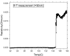
produced by the solid-phase method in Example 4, where the Tc_III phase with
the
highest critical temperature was dominant. The critical temperature of the
ceramic
material was found to exceed -104 C.
Experimental Example 10. Analysis of composition of the ceramic material
produced by solid-state reaction
The composition of the ceramic material produced in Example 4 was analyzed
by FE-SEM/EDX. The results are shown in Figs. 24 to 27. Referring to the SEM
images,
the surface morphology of the ceramic material produced in Example 4 was
similar to
that of the ceramic material produced in Example 1. Referring to Fig. 28, the
structure of
the inventive ceramic material (LK99) was different from that of apatite.
Fig. 41 is a table showing the atomic ratios of the elements constituting the
ceramic material produced in Example 4.
Experimental Example 11. Measurement of electrical properties of the
ceramic material produced by solid-state reaction
The ingot prepared by the solid-state reaction in Example 4 was processed into
a
rectangular shape and its resistances were measured with varying temperatures
(304-382
K) by a 4-probe method using a KEITHLEY 228A power (voltage/current) source
and a
KEITHLEY 182 sensitive digital voltmeter. The results are shown in Fig. 29.
Referring
to Fig. 29, the inventive ceramic material showed superconductivity.
Fig. 42 is a photograph showing an experiment for measuring the resistance of
the ceramic material in real time. The measured resistances were as low as
approximately
10-12-10-10 Ohm=cm.
Experimental Example 12. Crystal structure of the ceramic material
produced by solid-state reaction
The crystal structure of the ceramic material produced in Example 4 was
analyzed by XRD using a multi-purpose X-ray diffractometer (PHILIPS). The
results are
shown in Fig. 30. Referring to Fig. 30, the structure of the ceramic material
(LK99) was
31
CA 03228919 2024-02-08
= =
different from that of apatite.
Industrial applicability
The superconductivity of the ceramic material according to the present
invention
has been demonstrated with a partially filled SQW model. The ceramic material
of the
present invention will be a very useful material for the study of
superconductivity puzzles
at room temperature. All evidence and explanation lead to the conclusion that
LK-99 is
the first room-temperature and ambient-pressure superconductor. Therefore, it
can be said
that LK-99 is applicable to a wide variety of fields, including magnets,
motors, cables,
levitation trains, power cables, qubits for quantum computers, and THz
antennas.
32