Note: Descriptions are shown in the official language in which they were submitted.
WO 2023/039095
PCT/US2022/042948
Q-BAND BLOCK DOWN CONVERTER
CROSS-REFERENCE TO RELATED APPLICATIONS
[0001] This application claims the benefit of priority to U.S. Provisional
Patent
Application No. 63/242,438, filed on September 9, 2021, the entire contents of
which are
incorporated by reference herein.
FIELD
[0002] This specification generally describes technology related to providing
improved
down converters for communication systems, such as for gateways of satellite
networks.
BACKGROUND
[0003] In a satellite communication system, a gateway is used as a ground
station to
connect a terrestrial network, such as the Internet, and satellites orbiting
Earth. For example,
the gateway can transmit data from user terminals or other devices to the
orbiting satellites.
Further, the gateway can receive data from the orbiting satellites and relay
the data to the
terrestrial network. The gateway uses antennas and other equipment for
converting,
transmitting, and receiving signals. For example, the gateway typically
includes a down
converter to convert high-frequency radiofrequency (RF) signals received by an
antenna to
lower-frequency RF signals for demodulation and other processing.
SUMMARY
[0004] In some implementations, a receive chain for a satellite gateway
includes a block
down converter configured to down convert an RF input signal in the Q band to
an
intermediate frequency (IF) signal in the S band. The down converter can
include various
features that can provide high performance in converting Q-band signals. For
example, the
down converter can employ a single mixer stage, which can minimize phase noise
and other
types of noise. As another example, the down converter can generate a local
oscillator signal
for the mixer using a series of multiple phase-locked loops (PLLs), to
progressively increase
the frequency with high accuracy. In addition, the output of the series of
PLLs can be further
increased using a frequency multiplier, to obtain the final local oscillator
signal input to the
mixer.
[0005] As another example, the down converter can include one or more
temperature
compensation elements that compensate for changes in gain that are induced by
changes in
CA 03230975 2024- 3-5
WO 2023/039095
PCT/US2022/042948
temperature. In some implementations, multiple temperature compensation
elements are
included at different portions of the signal path through the down converter,
enabling the
down converter to achieve and maintain desired gain levels . In some
implementations, the
temperature compensation in the down converter provides temperature stability
so that gain
does not increase or decrease by more than 1 dB across a temperature range
from 20 C to
40 C.
[0006] In some implementations, a radiofrequency down converter includes: an
input port
to receive a radiofrequency input signal; a first bandpass filter comprising a
microwave
waveguide, the first bandpass filter being coupled to the input port and being
configured to
filter the radiofrequency input signal; a mixer stage coupled to the first
bandpass filter, the
mixer stage being configured to generate a mixer output signal by processing
the filtered
radiofrequency input signal using a gain adjustment device, one or more
amplifiers, and a
frequency mixer; a signal adjustment stage coupled to receive the mixer output
signal, the
signal adjustment stage comprising: a temperature compensation device
configured to
compensate for changes in signal gain or attenuation due to changes in
temperature; a second
bandpass filter; a gain adjustment device; one or more amplifiers; and a low
pass filter; and
an output port coupled to output an adjusted mixer output signal from the
signal adjustment
stage.
[0007] Implementations may include one or more of the following features. For
example,
in some implementations, the signal adjustment stage further comprises a gain
slope
compensation device configured to reduce variation in frequency response gain
across
frequencies in the adjusted mixer output signal.
[0008] In some implementations, the temperature compensation device is a first
temperature compensation device; the signal adjustment stage further comprises
a second
temperature compensation device; and the first temperature compensation device
is coupled
to receive input based on the mixer output signal and provide a first
compensated signal to
the second bandpass filter, and wherein the gain adjustment device is coupled
to receive
signals that are based on output of the second bandpass filter, and wherein
the second
temperature compensation device is coupled to provide output used to provide
input to the
low pass filter.
100091 In some implementations, the radiofrequency down converter includes a
microwave
isolator located between the first bandpass filter and the mixer stage, the
microwave isolator
being configured to propagate microwave signals from the first bandpass filter
to the mixer
2
CA 03230975 2024- 3-5
WO 2023/039095
PCT/US2022/042948
stage and to block propagation of microwave signals from the mixer stage to
the first
bandpass filter.
[0010] In some implementations, the radiofrequency down converter is
configured to
downconvert an input signal in a band within a range from 36 GHz to 46 GHz to
an
intermediate frequency signal in a band within a range from 1 GHz to 6 GHz.
[0011] In some implementations, the radiofrequency down converter is
configured to
downconvert input signals from 40 GHz to 42 GHz to an intermediate frequency
of 2 GHz to
4 GHz.
[0012] In some implementations, the radiofrequency down converter includes: a
reference
frequency port to receive a reference frequency signal; and a frequency
generating stage
coupled to receive the reference frequency signal, the frequency generating
stage comprising
at least one phase-locked loop, the frequency generating stage being
configured to provide an
output signal that is used to provide a local oscillator signal that is
provided to the frequency
mixer.
[0013] In some implementations, the radiofrequency down converter includes a
frequency
multiplier device coupled to receive the output signal of the frequency
generating stage and to
generate the local oscillator signal, wherein the local oscillator signal has
a frequency that is
greater than the frequency of the output signal of the frequency generating
stage by a
predetermined multiple.
[0014] In some implementations, the frequency generating stage is configured
to receive a
reference signal at substantially 10 Ghz; the frequency generating stage is
configured to
output the output signal of the frequency generating stage at substantially
9.5 GHz; and the
frequency multiplier device is configured to output the local oscillator
signal at substantially
38 GHz.
[0015] In some implementations, the frequency generating stage comprises a
first phase-
locked loop coupled to receive the frequency reference signal, a second phase-
locked loop
coupled to receive output of the first phase-locked loop, and a third phase-
locked loop
coupled to receive output of the second phase-locked loop. The first phase-
locked loop is a
digital phase-locked loop, wherein the second phase-locked loop that is a
cleanup phase-
locked loop, and wherein the third phase-locked loop configured to provide the
output signal
for the frequency generating stage at a predetermined frequency.
[0016] In some implementations, the radiofrequency down converter includes an
oven-
controlled crystal oscillator coupled to provide an output signal to the first
phase-locked loop.
3
CA 03230975 2024- 3-5
WO 2023/039095
PCT/US2022/042948
[0017] In some implementations, the temperature compensator device is
configured to
compensate for changes in signal gain due to changes in temperature caused by
the oven-
controlled crystal oscillator.
[0018] In some implementations, the radiofrequency down converter includes: a
monitoring port coupled to provide external output of the output signal
provided by the
frequency generating stage; and a test port coupled to provide external output
of the adjusted
mixer output signal.
[0019] In another general aspect, a method includes: generating a first
oscillator signal at a
predetermined frequency using one or more phase-locked loops of a down
converter;
generating a second oscillator signal that is a multiple of the first
oscillator signal using a
frequency multiplier of the down converter; receiving a radiofrequency signal
at an input of
the down converter; filtering the radiofrequency signal using a waveguide
roofing filter of the
down converter; mixing the filtered radiofrequency signal with the second
oscillator signal
using a frequency mixer of the down converter; compensating for temperature-
induced
changes in gain using one or more temperature compensation elements to signals
generated
of the frequency mixer; filtering output of the frequency mixer using a
bandpass filter of the
down converter and a low pass filter of the down converter to generate an
intermediate
frequency signal; and outputting the intermediate frequency signal as an
output of the down
converter.
[0020] Implementations may include one or more of the following features. For
example,
in some implementations, the method includes receiving input of a reference
signal at a first
frequency, and generating the first oscillator signal comprises generating the
first oscillator
signal using a series of multiple phase-locked loops that increase in
frequency over multiple
stages, the first oscillator signal being generated in alignment with respect
to the reference
signal.
100211 In some implementations, adjusting gain applied to signals output from
the
frequency mixer in response to a control signal from one or more processors of
the down
converter.
[0022] In some implementations, the down converter comprises multiple
temperature
compensation elements placed at different positions in a signal path through
the down
converter to adjust for temperature-induced variation of signal gain of
different components
of the down converter.
4
CA 03230975 2024- 3-5
WO 2023/039095
PCT/US2022/042948
[0023] In some implementations, the down converter is configured to
downconvert an
input signal in a band within a range from 36 GHz to 46 GHz to an intermediate
frequency
signal in a band within a range from 1 GHz to 6 GHz.
[0024] In some implementations, the down converter is configured to
downconvert input
signals from 40 GHz to 42 GHz to an intermediate frequency of 2 GHz to 4 GHz.
[0025] In some implementations, the down converter is configured to generate
the first
oscillator signal synchronized with a reference signal at substantially 10
Ghz; wherein the
second oscillator signal has a frequency of substantially 9.5 GHz; and wherein
the frequency
multiplier is configured to output the second oscillator signal at
substantially 38 GHz.
[0026] Other embodiments of these aspects include corresponding systems,
apparatus, and
computer programs, configured to perform the actions of the methods, encoded
on computer
storage devices. A system of one or more computers can be so configured by
virtue of
software, firmware, hardware, or a combination of them installed on the system
that in
operation cause the system to perform the actions. One or more computer
programs can be
so configured by virtue having instructions that, when executed by data
processing apparatus,
cause the apparatus to perform the actions.
[0027] The details of one or more implementations are set forth in the
accompanying
drawings and the description below. Other potential features and advantages
will become
apparent from the description, the drawings, and the claims.
BRIEF DESCRIPTION OF THE DRAWINGS
[0028] FIG. 1 is a diagram that illustrates an example of an antenna and
receive chain for a
satellite gateway.
[0029] FIG. 2 is a diagram that illustrates an example of a down converter of
the receive
chain of FIG. 1.
100301 FIG. 3 is a block diagram that illustrates additional features of the
down converter.
[0031] FIG. 4 is a diagram that illustrates additional components of the down
converter.
[0032] FIG. 5 is a perspective cutaway view of the down converter.
[0033] FIG. 6 is a front view that illustrates a panel of the down converter.
100341 In the drawings, like reference numbers represent corresponding parts
throughout.
DETAILED DESCRIPTION
[0035] FIG. 1 shows an example antenna 100 of a satellite gateway. The
satellite gateway
is a ground station that provides the link between a satellite network and a
terrestrial network.
CA 03230975 2024- 3-5
WO 2023/039095
PCT/US2022/042948
For example, the satellite gateway uses the antenna 100 to transmits data from
a core network
(e.g., a wide area network (WAN), the Internet, etc.) to one or more
satellites for downlink
transmission to terminals (e.g., very small aperture terminals (VSATs)). The
satellite
gateway also uses the antenna 100 to receive uplink data from terminals via
the one or more
satellites and provides the uplink data to the core network.
[0036] The antenna 100 includes a dish 102, a hub section 104, and
a pedestal 106. The
antenna 100 can be configured to house various electronics within it. For
example,
components of a receive chain can be configured to be placed in the antenna
100. The
illustrated example shows a series of components that form a receive chain,
and which may
be designed and sized to be housed within the antenna 100.
[0037] The components of the receive chain are illustrated in two different
groups. A first
group of hub components 110 are located in the hub 104. The hub components 110
include
radiofrequency (RF) components including a down converter. A second group of
pedestal
components 150 is configured to receive and process an intermediate frequency
signal and
includes components such as a modem.
[0038] The antenna 100 can be configured to receive signals in the microwave
region of
the electromagnetic spectrum, such as signals in the Q band, which used herein
refers to the
range of 33-50 GHz. While the examples discussed herein focus on the Q band,
the
techniques used in the antenna 100 and its associated devices like the Q-band
block down
converter (QBDC) 130 can be applied to receive signals in other bands. The
antenna 100
can, of course, be created for and used in more narrow ranges such as the Q
band definition
of 36-46 GHz set by the International Organization for Standardization (ISO).
More
generally, the antenna 100 can be designed to operate in the extremely high
frequency (EHF)
range designation of the International Telecommunication Union (ITU), and in
the Ka band
(26.5-40 GHz) and/or V band (40-75 GHz) defined by the Institute of Electrical
and
Electronics Engineers (IEEE).
[0039] The QBDC 130 can be configured to down convert input in the Q band to
an
intermediate frequency in the S band (e.g., 2-4 GHz). However, by changing the
local
oscillator signals used for mixing and using appropriate filters, the
techniques discussed
herein can be used to downconvert to other bands such as the L band (e.g., 1-2
GHz), C band
(e.g., 4-8 GHz), or other band as appropriate for reception.
[0040] Operating a down converter at microwave frequencies, such as the Q-
band, can
create various challenges for traditional down converter designs. For example,
many receiver
components and mixer designs create significant amounts of noise, especially
phase noise,
6
CA 03230975 2024- 3-5
WO 2023/039095
PCT/US2022/042948
that can impede proper reception of Q-band signals. This issue often becomes
more
dominant as the frequency of the signals increases, and can be much more
significant for
receiving Q-band signals than for K-band signals and lower Ka-band signals. In
addition,
generating a stable and accurate local oscillator signal for frequency mixing
is more
challenging for an oscillator signal in the Q-band than for lower-frequency
bands.
[0041] Effective reception of high frequency RF signals, such as Q-band
signals, often
requires very accurate, high-performing systems. In many cases, providing
amplifiers and the
down converter as close to the antenna as possible. Maximizes the quality of
reception. For
example, providing the low noise amplifier 120 and the QBDC 130 in the hub of
the antenna.
100 minimizes signal loss and maximizes the quality of reception. However,
receive chain
components such as the QBDC are often sensitive to temperature changes, which
can affect
their performance. As discussed for their below, with respect to FIG. 4, the
QBDC 130 can
include a number of features to achieve high performance even when exposed to
the
temperature changes that occur in an outdoor environment or other environment
that is not
temperature-controlled.
[0042] As will be discussed further below, the antenna 100 can be designed to
receive
signals in the range of 40-42 GHz (e.g., a bandwidth of 2 GHz centered at 41
GHz). To
receive the signal, the Q-band block down converter (QBDC) 130 can convert
from the RF
input frequency range of substantially 40-42 GHz to an intermediate frequency
(IF) range of
substantially 2-4 GHz. The QBDC 130 can use a single mixer stage to minimize
phase noise,
and can use a very high-accuracy and high-stability local oscillator signal of
substantially 38
GHz. As used herein, a frequency or frequency range boundary at "substantially-
a particular
frequency can encompass frequencies within 10% of the specified frequency,
although the
design can be set with values that are closer to the specified frequency
(e.g., within 5%,
within 1%, within 0.1%, etc.). In addition, many other variations of the
frequency plan
discussed herein can be used. For example, the QBDC 130 can be designed to
receive RF
signals with a center frequency that is lower than 41 GHz (e.g., 40 GHz, 38
GHz, 36 GHz, 35
GHz, etc.) or higher than 41 GHz (e.g., 42 GHz, 44 GHz, 46 GHz, 48 GHz, etc.).
Similarly,
the bandwidth for received RF signals can be greater than 2 GHz (e.g., 2.5
GHz, 3 GHz, 3.5
GHz, 4 GHz, etc.) or less than 2 GHz, (e.g., 1.5 GHz, 1.0 GHz, etc.). The QBDC
130 can
also be built to support different IF frequencies, including variation in
center frequency
and/or bandwidth. For example, rather than a center frequency at 3 GHz and a
bandwidth of
2 GHz, the intermediate frequency signals may have a center frequency that is
higher (e.g.,
7
CA 03230975 2024- 3-5
WO 2023/039095
PCT/US2022/042948
3.5 GHz, 4 GHz, etc.) or lower (e.g., 2.5 GHz, 2 GHz, etc.), and the bandwidth
may be higher
(e.g., 2.5 GHz, 3 GHz, 3.5 GHz, etc.) or lower (e.g., 1.75 GHz, 1.5 GHz, 1
GHz, etc.).
[0043] The local oscillator signal can be generated using a multi-stage
frequency generator
that uses multiple phase-locked loops (PLLs) and a frequency multiplier to
generate the local
oscillator signal. In addition, the generated frequency can be locked or
synchronized to an
input frequency reference at a much lower frequency, such as 10 MHz, which can
help the
system to drive multiple device or units together on a single frequency
reference source. For
example, multiple QBDC 130 units of a gateway can be synchronized using a
common
external 10 MHz reference (e.g., using a single source for the reference). In
many cases, the
modems of a gateway, such as the modem 156, can also use the same common
reference as
the QBDCs 130. Thus, all components are synchronized so there is no frequency
offset.
[0044] In further detail, an antenna feed 114 provides the RF signal received
using the dish
102. Impedance matching networks or other components can be included, such as
a standing
wave ratio meter 116. Next, a port 118 or tap is provided to enable monitoring
of the signal
being received and propagated. The RF signal is propagated to a low noise
amplifier 120 that
amplifies the signal. After the low noise amplifier 120, another port 122 is
provided for
monitoring and testing. The amplified signal from the low noise amplifier 120
is propagated
further to a block down converter, in this case, a Q-band block down converter
(QBDC) 130,
which will be discussed in detail below. After the QBDC 130, another port 132
is provided,
which can be used to monitor the intermediate frequency (IF) output of the
QBDC 130.
[0045] The pedestal components 150 receive the IF output from the QBDC 130. A
cable
152, such as a coaxial cable, can provide the IF signal to a divider 154, and
the divided signal
is provided to a modem 156. Output from the modem 156 is provided to a
network, such as a
core network, a wide area network (WAN), the Internet, or another public
network.
[0046] FIG. 2 shows various inputs and outputs of the QBDC 130. The QBDC 130
has an
RF input port to receive RF input 202. In the example, the RF input signal to
be received is
substantially from 40 to 42 GHz. Of course, the QBDC 130 can be designed and
used to
receive a larger or smaller range of bandwidth, and may be designed and used
to receive
higher or lower frequencies, including in bands below the Q band.
Nevertheless, because the
demands on receivers typically increase as the input frequency increases, the
QBDC 130 is
especially suited for high performance with relatively high RF bands, such as
the Q band.
[0047] The QBDC 130 has ports for a number of different outputs. These include
an
intermediate frequency output 208, which in this case is substantially 2-4
GHz. The outputs
include a local oscillator monitoring port ("LO MON") that provides a signal
related to the
8
CA 03230975 2024- 3- 5
WO 2023/039095
PCT/US2022/042948
local oscillator input to the mixer. In some implementations, the LO MON 204
is not the
same frequency provided as input to the mixer, but instead is a fraction of
that frequency
(e.g., one fourth of the oscillator signal), as discussed with respect to FIG.
4 below. For
example, the LO MON 204 signal can be a generated frequency prior to a
frequency
multiplication stage used to generate the final local oscillator signal input
to the mixer. The
outputs also include a test output 208 that can be used to test output of the
QBDC 130.
[0048] The QBDC 130 also receives a frequency reference signal 210, which is
used to
generate the local oscillator signal used by the mixer. The QBDC 130 also
includes a network
interface so that bi-directional communication over a local area network (LAN)
212 is
provided. This network connection can facilitate monitoring, configuration,
status checking,
and other operations in combination with a remote system.
[0049] FIG. 3 is a block diagram of the QBDC 130, showing several of the
assemblies
within the QBDC 130. For example, the QBDC 130 includes a microwave assembly
302 that
receives the RF input 202 and provides the IF output 208. The microwave
assembly 302 also
receives the frequency reference signal 210 as input, and provides other
outputs including the
LO MON 204 and test 206 outputs. The QBDC 130 also includes a controller
assembly 304,
which includes a microcontroller board. The controller assembly 304 monitors
the operation
of the microwave assembly 302 and performs control functions to configure and
adjust
operation of the microwave assembly 302 as needed. The controller assembly 304
receives
signals over the LAN 212, and can provide status information over the LAN 212
as well as
receive instructions and requests to adjust operation of the QBDC 130. The
QBDC 130 also
includes a power supply 306, which receives alternating current (AC) and
provides direct
current (DC) output to power the controller assembly 304 and the microwave
assembly 302.
[0050] As shown in FIG. 3, the RF input 202 can be a signal having a bandwidth
of
substantially 2 GHz around a center frequency such as a 41 GHz. As a result,
the input signal
to be received is in the range of substantially 40 to 42 GHz. The microwave
assembly 302 of
the QBDC 130 down converts from the Q-band RF input 202 to an IF output 208 of
substantially 2-4 GHz.
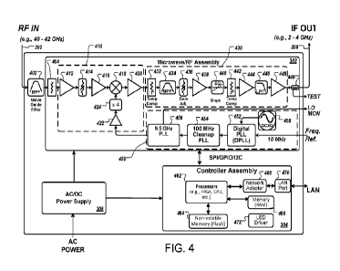
[0051] FIG. 4 shows a more detailed diagram of the QBDC 130. For example, the
microwave assembly 302 can include sections such as a mixer stage 410, a set
of signal
adjustment components 430 that receive output of the mixer stage 410, and a
frequency
generator 450. The QBDC 130 can also include various other signal processing
elements as
discussed below.
9
CA 03230975 2024- 3-5
WO 2023/039095
PCT/US2022/042948
[0052] The QBDC 130 is configured to down convert from the Q-band RF input
signal 202
to the IF output signal 208. Because Q-band signals are at a much higher
frequency than
many other frequency bands often used, reception is often impacted much more
by any offset
or jitter in the local oscillator frequency, by temperature-induced gain
variation in amplifiers,
and other factors. The QBDC 130 is designed to compensate for many of the
effects that
would normally reduce the performance of a receiver processing a Q-band
signal. Some of
the features that enhance reception of Q-band signals include the single mixer
stage (as
opposed to a multi-stage mixer design), the use of temperature compensation to
compensate
for temperature-induced change in gain in amplifiers and other components, and
a very high-
precision system for generating the local oscillator signal for frequency
mixing. These and
other aspects of the design enable very high performance at Q-band
frequencies, to minimize
phase noise and other effects that could otherwise impede reception.
100531 As an initial component to receive the RF input 202, the RF receive
chain can
include an isolator (not shown) at the input where the RF input 202 is
received. The isolator
can he a waveguide isolator, such as a microwave circulator with a load
attached. The isolator
can act as a one-way valve for energy to block power being transmitted back
toward the
antenna. As examples, the isolator can be a ferrite-based isolator, a
terminated circulator, a
Faraday rotation isolator, a field-displacement isolator, or a resonance
absorption isolator.
[0054] Next, the RF input 202 is filtered using a band pass filter 402. This
bandpass filter
402 can be a roofing filter designed to limit the pass band to the desired
signal region, in this
case, substantially 40 GHz to 42 GHz. The bandpass filter 402 can be
implemented as a
waveguide filter, and may include multiple stages, for example, between 9 to
11 stages in
some implementations.
[0055] After the bandpass filter 402, the filtered signal is provided to an
isolator 404, and
then passed to the mixer stage 410. The QBDC 130 is can operate with a single
mixer stage
410, which includes a single frequency mixer 418. The mixer stage 410 includes
an amplifier
412, a gain adjustment device 414, and amplifier 416, the frequency mixer 418,
and an
amplifier 420.
[0056] The mixer stage 410 includes a single frequency mixer element 418 to
process the
RF input signal. Using only a single mixer 418 in the signal path helps
minimize the amount
of noise that is added, especially to minimize phase noise. The mixer element
418 receives
the output of the amplifier 416 and also receives a local oscillator signal.
The local oscillator
signal is generated by the frequency generator 450 and a frequency multiplier
424. In
particular, the illustrated example has a 9.5 GHz signal output from the
frequency generator
CA 03230975 2024- 3-5
WO 2023/039095
PCT/US2022/042948
450, and the frequency multiplier 424 multiplies this signal by a factor of 4,
to obtain a local
oscillator signal of 38 GHz. The mixer element 418 thus produces a lower side
band at the
desired intermediat frequency from 2-4 GHz, e.g., a center at 3 GHz and a
bandwidth of 2
GHz.
[0057] In many cases, a very stable, highly-accurate oscillator signal is
important for
accurate downconversion of Q-band signals. To provide a high-quality
oscillator signal, the
frequency generator 450 includes multiple phase-locked loops (PLLs), and does
not attempt
to create the 38 GHz signal in a single stage. Instead, the frequency
generator 450 uses
multiple stages to generate a 9.5 GHz signal with very high accuracy and
stability, and the
frequency multiplier 424 boosts the frequency to the final oscillator signal
desired, e.g., at 38
GHz.
[0058] The frequency generator 450 is configured to receive a
frequency reference signal
210 at a predetermined frequency, which is substantially 10 GHz in the
example. The
reference frequency signal 210 is then generated a first PLL, a second PLL
454, and a third
PLL 456. The series of PLLs provides a high-quality oscillator signal at the
desired level for
input to the frequency multiplier 424.
[0059] The frequency generator 450 can include an oven-controlled crystal
oscillator
(OCXO) 458, which may be used in lieu of the external 10 MHz reference. The
OCXO has
ultra-low phase noise and is extremely stable over temperature. In normal
operation, the
QBDC's Q-band frequency source is locked to the external 10 MHz reference.
Monitor and
control circuitry continually checks health and stability of the external 10
MHz reference and
the internal OCXO. If the external 10 MHz signal is lost, the monitoring and
control circuitry
transitions to the internal OCXO with smooth continuation, e.g., a hitless
transition that
maintains a consistent reference without interruption. When the external 10
MHz reference
signal returns, the M&C circuitry switches back to the external reference,
again in a hitless
transition that maintains the reference signal input at the appropriate
frequency to the first
PLL 452.
[0060] The frequency generator 450 operates the first PLL 452 at 10 MHz, the
second PLL
454 at 100 MHz, and the third PLL at 9.5 GHz. As a result, the input frequency
reference 210
is increased in frequency by a factor of 10 at the second PLL 454 and the
output of that PL is
increased in frequency again by a factor of 95 at the third PLL 456. The
design of the
frequency generator 450 sides a very low noise local oscillator source that is
locked to the
incoming 10 MHz reference. The frequency generator 450 also provides tolerance
to short-
11
CA 03230975 2024- 3-5
WO 2023/039095
PCT/US2022/042948
term loss of the reference signal 210, to be able to maintain the reference
signal even through
an interruption or disconnection of the reference for a few seconds.
[0061] The first PLL 452 can be a digital PLL. The PLL 452 receives, in
addition to the
frequency reference signal 210, output of an oven-controlled crystal
oscillator (OCX0) 458.
The OCXO 458 can include a temperature-controlled chamber used to maintain the
crystal of
the oscillator at a consistent temperature, to minimize changes in frequency
due to changes in
ambient temperature.
[0062] The output of the first PLL 452 is provided to the second PLL 454,
which can be a
cleanup PLL providing output at 100 MHz. The output of the second PLL 454 is
provided to
the third PLL 456, which outputs a 9.5 GHz output signal.
[0063] The output of the frequency generator 450 is received by an amplifier
422 in the
mixer stage 410. The amplified 9.5 GHz signal is provided to the frequency
multiplier 424,
which is configured to increase the frequency by an integer multiple. In this
case, the
frequency multiplier 424 creates the local oscillator signal by multiplying
the 9.5 GHz input
by a factor of 4.
[0064] After frequency mixing occurs at the frequency mixer 418, and that
output is
amplified by the amplifier 420, the signal adjustment components 430 process
the output
further. These components 430 perform functions such as signal amplification,
gain control
(e.g., adjustable gain in a range spanning at 10 dB, 20 dB, 25 dB, or more),
intermediate
frequency filtering, image frequency, rejection, and rejection of the local
oscillator, gain
slope correction, and compensation for variation in gain due to temperature
changes.
[0065] To describe the signal adjustments components 430 further, the
amplified mixer
output is provided to a first temperature compensation element 432. This
element 432 is
configured to compensate for the variation in gain that can occur at different
temperatures. In
many cases, amplifier gain is affected by temperature, and so the temperature
compensation
element 432 can correct for this effect. The temperature compensation element
can be an
attenuator circuit chip with a negative temperature coefficient. For example,
for many
radiofrequency and intermediate-frequency elements, attenuation decreases (or
gain
increases) as temperature increases. To compensate for this, attenuation
circuits that have the
opposite property, e.g., attenuation increases as temperature increases, can
be provided as
temperature compensation elements.
[0066] In general, the temperature compensation element 442 can be configured
to perform
a temperature-dependent amount of power dissipation complementary to the
temperature-
dependent gain or dissipation of other devices in the QBDC 130, so that the
overall gain or
12
CA 03230975 2024- 3-5
WO 2023/039095
PCT/US2022/042948
attenuation varies minimally with temperature. The temperature compensation
element 442
can be implemented using active components or passive components. For example,
active
compensation can be performed using a temperature sensor to measure a
temperature, and
transistors and other circuit components to change gain or attenuation based
on the measured
temperature. As another example, a passive temperature-compensating attenuator
can
include a network of thermistors to provide a response that varies with
temperature, such as a
network of thick-film thermistors deposited on an alumina substrate.
[0067] Output of the temperature compensation element 432 is provided to a
band pass
filter 434. The band pass filter 434 can be configured to reject the upper
side band (e.g.,
centered at 79 GHz, extending from 78-80 GHz) as well as the local oscillator
frequency
(e.g., 38 GHz). Because the local oscillator frequency and the upper side band
are so far
above the lower side band that provides the desire intermediate frequency, the
band pass filter
434 can have a larger passband than the 2-4 GHz range, to ensure that the
filter 434 does not
attenuate desired IF signals.
[0068] After filtering with the hand pass filter 434, the filtered signal is
provided to a gain
adjustment element 436, which allows for a significant amount of gain
adjustment. For
example, the gain adjustment element 436 can provide adjustable gain, as
instructed or
controlled using the controller assembly 304. The gain adjustment element 436
can support a
range of gain levels, such as a range that spans at least 10 dB, 15 dB, 20 dB,
25 dB, 30 dB or
another appropriate level. For example, the gain adjustment element 436 can
enable gain to
be adjusted over a range from 0-25 dB in steps of ldB or less (and in some
cases steps of 0.2
dB or less), leading to an overall gain for the QDBC 130 as a whole that is
selectable from a
range of substantially 5-30 dB. As used here, the term "substantially" can
encompass a value
that is 10% greater or lower than specified, although the range can be set
with greater
specificity (e.g., within 5%, within 1%, within 0.1%, etc.).
100691 Output from the gain adjustment element 436 is provided to another
amplifier 438,
which provides output to a gain slope correction element 440. Because
amplifier gain can be
different for different frequencies, the gain slope correction element 440 can
be configured to
apply compensation (e.g., a fixed amount of compensation based on overall
characteristics of
the receive chain) to equalize gain across the frequencies in the desired IF
bandwidth range.
100701 The gain slope correction element 440 can be a circuit that equalizes
or flattens the
sloping gain across frequencies. In many cases, amplifiers have a gain versus
frequency
response that exhibits decreasing gain as frequency increases. When multiple
amplifiers are
cascaded, this can deepen the undesirable slope in the gain versus frequency
response. To
13
CA 03230975 2024- 3-5
WO 2023/039095
PCT/US2022/042948
equalize the gain, the gain slope correction element 440 can use active and/or
passive
techniques. For example, the gain slope correction element 440 can include an
attenuator
with a frequency response that slopes downward toward lower frequencies and
presents less
attenuation at higher frequencies. The attenuation slope can be set to
compliment the slope of
the amplifiers (e.g., one or more of amplifiers 438. 444, 448, or other
amplifiers) and other
components, then the overall frequency response of the combined circuits will
be relatively
flat. As another example, active gain equalizer circuits can be used to
provide a gain that
increases as frequency increases, to compensate for the overall gain of the
that would
otherwise decrease as frequency increases.
[0071] Output of the gain slope compensation element 440 is provided to a
second
temperature compensation element 442. Like the first temperature compensation
element
432, the second temperature compensation element 442 can adjust signal gain to
counteract
or compensate for variation in gain due to temperature. The technique of using
multiple
temperature compensation elements in the receive chain enables fine-tuned
control of
temperature-based gain compensation. For example, multiple temperature
compensation
elements provide the ability to more accurately maintain signal gain and
signal levels to
desired characteristics at multiple points within the receive chain, keeping
signal levels at
desired levels throughout the receive chain and not simply for the receive
chain as a whole. In
addition, multiple temperature compensation elements allow compensation to
take place at or
near the regions where affected amplifiers or other components are located,
thus
compensating for localized temperatures at different parts of the QBDC 130
itself For
example, the first temperature compensation element 432 can be used to adjust
for
temperature-induced gain variation in amplifiers 412, 416, and 420, while the
temperature
compensation element 442 may be located nearer to and may compensate better
for
temperature-induced gain variation in the amplifiers 438, 444, and 448. The
temperature at
the different sets of amplifiers may be different, and using separate
compensation elements
allows different adjustments for the sets of amplifiers having different
temperatures.
[0072] After the adjustment from the temperature compensation element 442, the
signal is
amplified with amplifier 444, and the amplified signal is provided to a low
pass filter 446.
The inclusion of the low pass filter 446, can further reduce or block
frequencies above the
desired range for IF output 208, such as blocking the upper side band from the
mixer element
418 and also the local oscillator signal. In some implementations, due to the
band pass filter
434 and the low pass filter 446, the level of rejection of image frequencies
and the local
oscillator signal at the output of the QBDC 130 is 50 dB or higher. Output of
the low pass
14
CA 03230975 2024- 3-5
WO 2023/039095
PCT/US2022/042948
filter 446 is provided to an amplifier 448 and provided as the IF output 208.
A port or tap
449 is provided after the amplifier 448.
100731 The controller assembly 304 includes one or more processors 462, such
as a field-
programmable gate array (FPGA), a central processing unit, microcontroller,
etc. The
controller assembly 304 includes non-volatile memory, such as NAND Flash
memory, to
store FPGA bistreams, software to be executed, configuration data, and so on.
The controller
assembly 304 also includes system memory, e.g., random access memory (RAM),
that the
processors 462 can use. The controller assembly 304 includes a network adapter
466 and a
LAN port 470 that enable the processors 462 to communicate with a network
management
system. For example, the processors 462 can provide status information over
the network, as
well as receive instructions, software, and configuration settings over the
network. The
processors 462 can be configured to monitor and adjust operation of the
microwave assembly
302, for example, to monitoring and adjust the level of gain applied, to
monitor operation and
status of different components, and so on. The processors 462 can communicate
with the
microwave assembly using a digital bus or other interface, such as a serial
peripheral
interface (SP1), general purpose input/output (GP10), Inter-Integrated Circuit
(12C) bus, etc.
100741 Using the architecture illustrated in FIG. 4, the QBDC 130 can be
configured to
provide the performance characteristics shown in the table below. These
characteristics are
provided as an example, but the techniques can be used advantageously for
other
configurations, such as other input frequency ranges, other output frequency
ranges, different
gain ranges, and so on.
Performance Parameter Characteristics Notes
RF Input Frequency Range 40.00 ¨ 42.01 GHz
IF Output Frequency Range 2.00 - 4.01 GHz
Gain Range 5 ¨ 30 dB in 0.2dB steps
Noise Figure < 15 dB At 30 dB gain
<1.0 dB peak-to-peak across any 200 MHz
band
Gain Flatness
<2.5 dB peak-to-peak Full 2.0 GHz band
Group Delay < 4 ns peak-to-peak In any 25 MHz BW
Gain Stability (Time) < 0.5 dB in 24 Hours At constant
temperature
Gain Stability (Temperature) < 0.75 dB 20 oC to 40 oC
CA 03230975 2024- 3-5
WO 2023/039095
PCT/US2022/042948
Input IP3 > -5 dBm
Spurious < -50 dBc
integrated from 500 Hz to 20
Phase Noise (DSB) < 1.0 deg RMS
MHz
In some implementations,
Image Rejection > 50 dB image rejection can
be 60 dB or
greater
Input Voltage Standing Wave
1.5:1 or less Zo = 50 ohm, (WR-22)
Ratio (VSWR)
Output Voltage Standing
1.5:1 or less Zo = 50 ohm, (N-f)
Wave Ratio (VSWR)
[0075] FIG. 5 shows an example of the controller assembly 304 and the
microwave
assembly 302 in a housing 500. The housing is configured to be removable from
the antenna
100 and also to be mountable to the antenna 100.
[0076] FIG. 6 shows a view of the ports at the exterior of the QBDC 130. The
housing 500
can include a panel 600 that provides access to the various ports and
indicator lights of the
QBDC 130. For example, the panel 600 includes an AC input port 602, an output
port 604
for output of the IF output 208, a test output port 606, a local oscillator
monitoring (LO
MON) port 607, a LAN port 608 (e.g., the LAN port 470 of FIG. 4), a reference
frequency
input port 610, and an RF input port 612. The panel 600 also includes a vent
614 and
indicator lights 616 to indicate power on status and operating status.
[0077] A number of embodiments have been described. Nevertheless, it will be
understood that various modifications can be made without departing from the
spirit and
scope of the invention. In addition, the logic flows depicted in the figures
do not require the
particular order shown, or sequential order, to achieve desirable results. In
addition, other
steps can be provided, or steps can be eliminated, from the described flows,
and other
components can be added to, or removed from, the described systems.
Accordingly, other
embodiments are within the scope of the following claims.
100781 A number of implementations have been described. Nevertheless, it will
be
understood that various modifications may be made without departing from the
spirit and
scope of the disclosure. For example, various forms of the flows shown above
may be used,
with steps re-ordered, added, or removed.
16
CA 03230975 2024- 3-5
WO 2023/039095
PCT/US2022/042948
[0079] Embodiments of the invention and all of the functional operations
described in this
specification can be implemented in digital electronic circuitry, or in
computer software,
firmware, or hardware, including the structures disclosed in this
specification and their
structural equivalents, or in combinations of one or more of them. Embodiments
of the
invention can be implemented as one or more computer program products, e.g.,
one or more
modules of computer program instructions encoded on a computer readable medium
for
execution by, or to control the operation of, data processing apparatus. The
computer
readable medium can be a machine-readable storage device, a machine-readable
storage
substrate, a memory device, a composition of matter effecting a machine-
readable propagated
signal, or a combination of one or more of them. The term "data processing
apparatus"
encompasses all apparatus, devices, and machines for processing data,
including by way of
example a programmable processor, a computer, or multiple processors or
computers. The
apparatus can include, in addition to hardware, code that creates an execution
environment
for the computer program in question, e.g., code that constitutes processor
firmware, a
protocol stack, a database management system, an operating system, or a
combination of one
or more of them. A propagated signal is an artificially generated signal,
e.g., a machine-
generated electrical, optical, or electromagnetic signal that is generated to
encode information
for transmission to suitable receiver apparatus.
[0080] A computer program (also known as a program, software, software
application,
script, or code) can be written in any form of programming language, including
compiled or
interpreted languages, and it can be deployed in any form, including as a
stand alone program
or as a module, component, subroutine, or other unit suitable for use in a
computing
environment. A computer program does not necessarily correspond to a file in a
file system.
A program can be stored in a portion of a file that holds other programs or
data (e.g., one or
more scripts stored in a markup language document), in a single file dedicated
to the program
in question, or in multiple coordinated files (e.g., files that store one or
more modules, sub
programs, or portions of code). A computer program can be deployed to be
executed on one
computer or on multiple computers that are located at one site or distributed
across multiple
sites and interconnected by a communication network.
100811 The processes and logic flows described in this specification can be
performed by
one or more programmable processors executing one or more computer programs to
perform
functions by operating on input data and generating output. The processes and
logic flows
can also be performed by, and apparatus can also be implemented as, special
purpose logic
17
CA 03230975 2024- 3-5
WO 2023/039095
PCT/US2022/042948
circuitry, e.g., an FPGA (field programmable gate array) or an ASIC
(application specific
integrated circuit).
[0082] Processors suitable for the execution of a computer program include, by
way of
example, both general and special purpose microprocessors, and any one or more
processors
of any kind of digital computer. Generally, a processor will receive
instructions and data
from a read only memory or a random access memory or both. The essential
elements of a
computer are a processor for performing instructions and one or more memory
devices for
storing instructions and data. Generally, a computer will also include, or be
operatively
coupled to receive data from or transfer data to, or both, one or more mass
storage devices for
storing data, e.g., magnetic, magneto optical disks, or optical disks.
However, a computer
need not have such devices. Moreover, a computer can be embedded in another
device, e.g.,
a tablet computer, a mobile telephone, a personal digital assistant (PDA), a
mobile audio
player, a Global Positioning System (GPS) receiver, to name just a few.
Computer readable
media suitable for storing computer program instructions and data include all
forms of non
volatile memory, media and memory devices, including by way of example
semiconductor
memory devices, e.g., EPROM, EEPROM, and flash memory devices; magnetic disks,
e.g.,
internal hard disks or removable disks; magneto optical disks; and CD ROM and
DVD-ROM
disks. The processor and the memory can be supplemented by, or incorporated
in, special
purpose logic circuitry.
[0083] To provide for interaction with a user, embodiments of the invention
can be
implemented on a computer having a display device, e.g., a CRT (cathode ray
tube) or LCD
(liquid crystal display) monitor, for displaying information to the user and a
keyboard and a
pointing device, e.g., a mouse or a trackball, by which the user can provide
input to the
computer. Other kinds of devices can be used to provide for interaction with a
user as well;
for example, feedback provided to the user can be any form of sensory
feedback, e.g., visual
feedback, auditory feedback, or tactile feedback; and input from the user can
be received in
any form, including acoustic, speech, or tactile input.
[0084] Embodiments of the invention can be implemented in a computing system
that
includes a back end component, e.g., as a data server, or that includes a
middleware
component, e.g., an application server, or that includes a front end
component, e.g., a client
computer having a graphical user interface or a Web browser through which a
user can
interact with an implementation of the invention, or any combination of one or
more such
back end, middleware, or front end components. The components of the system
can be
interconnected by any form or medium of digital data communication, e.g., a
communication
18
CA 03230975 2024- 3-5
WO 2023/039095
PCT/US2022/042948
network. Examples of communication networks include a local area network
("LAN") and a
wide area network ("WAN"), e.g., the Internet.
[0085] The computing system can include clients and servers. A client and
server are
generally remote from each other and typically interact through a
communication network.
The relationship of client and server arises by virtue of computer programs
running on the
respective computers and having a client-server relationship to each other.
[0086] While this specification contains many specifics, these should not be
construed as
limitations on the scope of the invention or of what may be claimed, but
rather as descriptions
of features specific to particular embodiments of the invention. Certain
features that are
described in this specification in the context of separate embodiments can
also be
implemented in combination in a single embodiment. Conversely, various
features that are
described in the context of a single embodiment can also be implemented in
multiple
embodiments separately or in any suitable subcombination. Moreover, although
features may
be described above as acting in certain combinations and even initially
claimed as such, one
or more features from a claimed combination can in some cases be excised from
the
combination, and the claimed combination may be directed to a subcombination
or variation
of a subcombination.
[0087] Similarly, while operations are depicted in the drawings in a
particular order, this
should not be understood as requiring that such operations be performed in the
particular
order shown or in sequential order, or that all illustrated operations be
performed, to achieve
desirable results. In certain circumstances, multitasking and parallel
processing may be
advantageous. Moreover, the separation of various system components in the
embodiments
described above should not be understood as requiring such separation in all
embodiments,
and it should be understood that the described program components and systems
can
generally be integrated together in a single software product or packaged into
multiple
software products.
[0088] In each instance where an HTML file is mentioned, other file types or
formats may
be substituted. For instance, an HTML file may be replaced by an XML, JSON,
plain text, or
other types of files. Moreover, where a table or hash table is mentioned,
other data structures
(such as spreadsheets, relational databases, or structured files) may be used.
100891 Particular embodiments of the invention have been described. Other
embodiments
are within the scope of the following claims. For example, the steps recited
in the claims can
be performed in a different order and still achieve desirable results.
[0090] What is claimed is:
19
CA 03230975 2024- 3-5