Note: Descriptions are shown in the official language in which they were submitted.
WO 2023/044452
PCT/US2022/076604
FIELD-SELECTABLE DYNAMIC GAIN CONTROL MODES OF OPTICAL
SENSORS
CROSS-REFERENCE TO RELATED APPLICATIONS
[0001] This application claims the benefit of U.S. Provisional Application
Serial No. 63/261,311,
titled -Field-Selectable Dynamic Gain Control Modes of Optical Sensors," filed
by Ashley Wise
on September 17, 2021.
[0002] This application incorporates the entire contents of the foregoing
application(s) herein by
reference.
[0003] The subject matter of this application may have common inventorship
with and/or may be
related to the subject matter of the following:
= U.S. Application Serial No. 15/625,949, titled "Open-Loop Laser Power-
Regulation," filed
by Ashley Wise on June 16, 2017, and issued as U.S. Patent No. 9985414 on May
29, 2018;
= U.S. Application Serial No. PCT/U521/71304, titled "Open-Loop Photodiode
Gain
Regulation,' filed by Ashley Wise, et al., on August 27, 2021;
= U.S. Application Serial No. 63/107,311, titled "Frequency Domain Opposed-
Mode
Photoelectric Sensor," filed by David S. Anderson, et al., on October 29,
2020;
= U.S. Application Serial No. 17/036,255, titled "Near Range Radar," filed
by Ashley Wise,
et al., on September 29, 2020;
= U.S. Application Serial No. 62/924,025, titled "Near Range Radar," filed
by Ashley Wise,
et al., on October 21, 2019;
= U.S. Application Serial No. 17/446,142, titled "Open-Loop Photodiode Gain
Regulation,"
filed by Ashley Wise, et al., on August 26, 2021; and
= U.S. Application Serial No. 63/071,080, titled "Open-Loop Photodiode Gain
Regulation,"
filed by Ashley Wise, et al., on August 27, 2020.
[0004] This application incorporates the entire contents of the foregoing
application(s) herein by
reference.
TECHNICAL FIELD
[0005] Various embodiments relate generally to gain control.
BACKGROUND
[0006] Photodiodes, including avalanche photodiodes (APDs), are employed in a
range of
applications. Applications may include, but are not limited to, presence and
positioning in
photoelectric sensors, distance measurement in triangulation and time of
flight sensors, and fiber-
optic communication.
1
CA 03231656 2024- 3- 12
WO 2023/044452
PCT/US2022/076604
[0007] In some examples, accuracy of distance measurement using APDs may be
affected by
reflectivity and distance of a target object. In some examples, a sensitivity
of the distance
measurement may also be affected by environmental parameters such as
temperature and ambient
light. Therefore, calibration may sometimes be applied to adjust a distance
sensor according to a
measurement environment.
SUMMARY
[0008] Apparatus and associated methods relate to a field selectable gain mode
system. In an
illustrative example, an APD-based sensor may, for example, have two or more
predetermined
gain modes. The gain modes may, for example, be activated in response to a
selection signal(s)
generated by a user. For example, the APD-based sensor may apply the user-
selected gain mode
by independently control a circuit gain, an emitter gain, and an APD gain.
When the user selection
signal is selected, for example, a controller may apply corresponding
independent gain parameters
to the circuit gain, the emitter gain, and the APD gain, such that a
collective high dynamic range
sensor system is provided. For example, the independent gain parameters may
include a range of
control voltages, a range of control current, and/or a range of gain input.
Various embodiments
may advantageously achieve increased accuracy across an extended operating
range of gain values
[0009] Various embodiments may achieve one or more advantages. For example,
some
embodiments may further generate a measurement offset profile based on the
user-selected gain
mode to advantageously maintain a high accuracy of measurement independent of
the user-
selected gain mode. Some embodiments may, for example, advantageously improve
gain
adjustment delays by comparing an updated set of gain parameters to an
original set of gain
parameters so that only the gain parameters with changes are applied. Some
embodiments may,
for example, generate at least one of the user-selectable gain modes based on
a measured
environmental parameter to advantageously maintain measurement accuracy
according to the
measured environmental parameter.
[0010] The details of various embodiments are set forth in the accompanying
drawings and the
description below. Other features and advantages will be apparent from the
description and
drawings, and from the claims.
BRIEF DESCRIPTION OF THE DRAWINGS
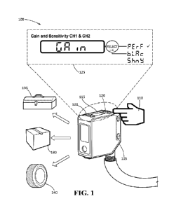
[0011] FIG. 1 depicts an exemplary selectable dynamic gain mode sensor (SDGMS)
employed in
an illustrative use-case scenario.
[0012] FIG. 2 depicts a block diagram of an exemplary SDGMS system.
[0013] FIG. 3 depicts an electrical block diagram of an exemplary SDGMS
system.
2
CA 03231656 2024- 3- 12
WO 2023/044452
PCT/US2022/076604
[0014] FIG. 4 depicts an exemplary limited dynamic range window which may be
expanded by
exemplary SDGMS systems.
[0015] FIG. 5 depicts an exemplary set of nominal user selectable gain mode
levels.
[0016] FIG. 6 depicts an exemplary amplitude plot of an exemplary high-
reflectivity (RR) gain
mode of an exemplary SDGMS.
[0017] FIG. 7 depicts an exemplary amplitude plot of an exemplary low-
reflectivity (LR) gain
mode of an exemplary SDGMS.
[0018] FIG. 8 depicts an exemplary SDGMS system control method.
[0019] FIG. 9A and FIG 9B depict an exemplary user interface interaction
process to field-adjust
a first channel of an exemplary SDGMS.
[0020] FIG. 10 depicts an exemplary user interface interaction process to
field-adjust a second
channel of the exemplary SDGMS.
[0021] Like reference symbols in the various drawings indicate like elements.
DETAILED DESCRIPTION OF ILLUSTRATIVE EMBODIMENTS
[0022] FIG. 1 depicts an exemplary selectable dynamic gain mode sensor (SDGMS)
employed in
an illustrative use-case scenario_ In an exemplary scenario 100, an SDGMS 105
may be operated
by a user 110 into a desired gain mode. The SDGMS 105 may have a user
interface including a
display 115. The interface may include user input elements 120 (e.g.,
buttons). The user 110 may
operate the user input elements 120 as shown in an exemplary interface display
125 to selectively
operate the SDGMS 105 into a predetermined dynamic gain mode. As depicted, by
way of example
and not limitation, the dynamic gain mode may include performance ("PErF"),
low-reflectivity
(LR) gain mode ("bLAc"), and high-reflectivity (HR) gain mode ("ShnY"). In
some embodiments
the performance mode may, by way of example and not limitation, be a default
mode.
[0023] The user 110 may, for example, operate the SDGMS 105 into a gain mode
appropriate for
a target object. rt he SDGMS 105 may, for example, be configured as a distance
sensor. The user
110 may select the HR gain mode when using the SDGMS 105 to detect the
distance to a highly
reflective target, such as a shiny metal target 135 (e.g., a polished metal
toolbox). The user 110
may select the performance (e.g., 'normal' gain) when using the SDGMS 105 to
detect the distance
to a normally reflective target, such as a cardboard box 130. The user 110 may
select the LR gain
mode when using the SDGMS 105 to detect the distance to a minimally reflective
target, such as
a black rubber tire 140. Accordingly, in various embodiments the SDGMS 105 may
advantageously be field adjusted into one of multiple (predetermined) dynamic
gain modes
according to a (currently) intended application.
3
CA 03231656 2024- 3- 12
WO 2023/044452
PCT/US2022/076604
[0024] Each (predetermined) dynamic gain mode may correspond to one or more
predetermined
settings. For example, when the SDGMS 105 is operated into a predetermined
gain mode, a control
unit of the SDGMS 105 may apply a predetermined gain mode profile to various
hardware and/or
software parameters. The gain mode profile may, for example, include emitter
power parameter(s).
The gain mode profile may, for example, include receiver drive control (e.g.,
drive voltage, drive
current) parameters. The gain mode profile may, for example, include at least
one calibration
profile. The calibration profile may, for example, include temperature
calibration. The calibration
profile may, for example, include voltage calibration. A predetermined gain
mode may, for
example, advantageously optimize the SDGMS 105 for a predetermined operation
mode. Within
a predetermined gain mode, the SDGMS 105 may advantageously dynamically adjust
gain within
a (predetermined) range. The dynamic gain range may, for example, be
determined as a function
of the gain mode profile.
[0025] For example, APDs may be used in a myriad of applications. APDs may, by
way of
example and not limitation, include single-photon avalanche diodes (SPAD).
APDs may, for
example, include silicon photomultipliers (SiPM). In some embodiments, APDs
may include, for
example, multi-pixel photon-counters (MPPC).
[0026] In various embodiments APDs may, for example, be applied to presence
measurement.
APDs may, for example, be applied to distance measurement. In some embodiments
a system
including an APD(s) may be configured as a time-of-flight sensor. In some
embodiments, APDs
may, for example, be used in fiber-optic communication implementations.
[0027] APDs may, for example, operate at a high reverse bias voltage. The
reverse bias voltage
may, by way of example and not limitation, include a range from 20 to 200
volts.
[0028] APDs may, for example, provide a current gain of a photoelectrical
current on the order of
Unity to 100s of times. When operated in Geiger mode, APD gain can, for
example, be thousands
to millions. In some embodiments, for example, current gain of an APD may be
embedded with
the photodetector. Such embodiments may, for example, advantageously provide
improved signal-
to-noise ratio relative to a photodetector with an external gain (such as a
trans-impedance amplifier
(TIA)). In some embodiments, a TIA(s) may be implemented to gain an output of
an APD.
[0029] APD gain may be proportional to the reverse bias voltage. If the
reverse bias voltage is too
low, the APD may not operate at all. If the reverse bias voltage is too high,
the APD may enter
Geiger mode (which may be unstable). Accordingly, various embodiments may
adjust the APD
gain up and down to accommodate a wide range of light intensity hitting the
APD. Adjusting the
gain of an APD may, for example, be accomplished by adjusting the reverse bias
voltage. In some
embodiments a time for (dynamic) APD gain adjustment to settle may be large.
For example, in
some embodiments a large APD gain adjustment time may be up to 250ms. For
example, to switch
4
CA 03231656 2024- 3- 12
WO 2023/044452
PCT/US2022/076604
from 100x gain to 10x gain, in some embodiments, may require waiting hundreds
of milliseconds
for the gain change to take effect. In some applications, however,
photoelectric sensors may be
required to operate with response speeds on the order of 250us to 5ms.
Therefore, a large APD
gain adjustment time may be too slow to happen during run mode operation
without disrupting the
sensor response time.
[0030] Various embodiments may advantageously operate the APD gain into a
predetermined gain
mode corresponding to a (limited) dynamic range. The output gain of the APD
may, for example,
be adjusted in the dynamic range. The APD may, for example, operate at a
predetermined reverse
bias voltage based on the currently selected gain mode. The APD may, for
example, operate in a
restricted reverse bias voltage range corresponding to a (predetermined)
maximum response time
and based on the currently selected gain mode. Accordingly, various
embodiments may
advantageously provide a wide gain range while achieving fast response times.
[0031] Dynamic range of light intensity hitting a photodiode (e.g., an APD)
may be quite large. In
some systems, for example, light may be emitted by a light emitting element
(e.g., laser, vertical-
cavity surface-emitting laser (VCSEL), edge emitting laser (EEL), LED), be
reflected off a target,
and a portion of this reflected light, including a diffuse component and a
specular component, may
be received on the APD.
[0032] In some embodiments, the SDGMS 105 may be configured with a gain mode
corresponding to "normal" targets having a reflectivity, by way of example and
not limitation,
between 3% to 90% diffuse reflection, with negligible specular reflection.
However, many
applications may demand sensing of a wider range of targets, such as, for
example, including clear
and high-angles (0.1%) and partially specular (1000%). This exemplary range of
reflectivity may
represent a 1:10000 dynamic range. Fully specular targets such as mirrors and
retro-reflectors may,
for example, require a dynamic range of 1:100000 or more.
[0033] Light intensity decreases by 1/D2 (where D = distance). Accordingly, a
low-reflectivity
target that requires 1:10000 dynamic range at distance D may require a dynamic
range of 1 :25 0000
at a second distance = 5 * D.
[0034] A dynamic range of an electronic circuit may, for example, be required
to match a needed
dynamic range of intended target(s). The dynamic range of the electronic
circuit may, for example,
be measured relative to a noise floor and/or baseline. This baseline/noise
floor may, for example,
be a minimum operating level (e.g., voltage, current, ADC value) at which a
signal can be
adequately distinguished from noise.
[0035] The dynamic range of an electronic circuit may, for example, be limited
at an upper end
by saturation. When a voltage, current, and/or ADC input is above a threshold,
the circuit may be
CA 03231656 2024- 3- 12
WO 2023/044452
PCT/US2022/076604
saturated, and the input cannot be measured any further. For a given
electronic circuit
configuration, a dynamic range may, for example, include saturation divided by
noise floor.
[0036] For a given electronic circuit configuration, a ratio of saturation to
noise floor may, by way
of example and not limitation, be between 1:50 to 1:200. In order to meet a
1:10000 minimum
dynamic range, for example, the circuit dynamic range may require being scaled
by changes in
gain. Increasing gain by a factor of 10, for example, could provide a dynamic
range of 1:500 to
1:2000 by gain change. In various embodiments, this principle may, for
example, advantageously
be applied to provide a circuit with a desired dynamic range (e.g., greater
than the example, lesser
than the example).
[0037] FIG. 2 depicts a block diagram of an exemplary SDGMS system. In the
depicted exemplary
SDGMS system 200, an emitter 205 is controlled by an emitter power module 210.
In the
illustrative depicted example, the emitter power module may, by way of example
and not
limitation, adjust emitter power by changing current to a laser. The emitter
power module may,
for example, provide between a 1:5 to 1:20 dynamic range in emitter power. In
various examples,
the emitter 205 may emit a signal (e.g., electromagnetic signal) towards a
target object 215. The
emitter 205 may, for example, include a photoelectronic emitter. The emitter
205 may, for
example, include a laser and the emitted signal may include an optical
beam(s). The emitter 205
may, for example, include an LED. The emitter 205 may, for example, emit a
pulsed signal. The
pulsed signal may, for example, be clocked. A monitor photodiode may, for
example, measure
characteristic(s) of' the emitted signal.
[0038] A receiver may, for example, receive a reflection of the emitted signal
reflected off of the
target object 215. The receiver may, for example, include a photodetector. The
photodetector may,
as depicted, include an avalanche photodiode (APD 220). The APD 220 is driven
by an APD
voltage 225 (e.g., reverse bias voltage). The APD voltage 225 may, for
example, represent a
dynamic gain range from 1:1 to 1:20, as depicted.
[0039] In the depicted example, electronic circuit gain is applied to an
output (e.g., voltage,
current) of the APD 220. As depicted, the electronic circuit gain may be
provided by a trans-
impedance amplifier (TIA 230). The TIA 230 may, for example, be implemented to
adjust a gain
of the output of the APD 220.
[0040] In the depicted example, electronic circuit gain may be provided by a
gain stage(s) (e.g.,
operational amplifier gain stage(s)) circuit(s) (gain stages 235). The stages
235 may, for example,
be implemented to adjust the gain of the output of the APD 220. In some
embodiments the stages
235 may operate directly on an output of the APD 220. In some embodiments the
stages 235 may,
for example, operate on an output of the TIA 230. The electronic circuit gain
(e.g., the TIA 230
6
CA 03231656 2024- 3- 12
WO 2023/044452
PCT/US2022/076604
and/or the stages 235) may, for example, provide between 1:5 to 1:20 dynamic
range in adjustable
gain.
[0041] An analog to digital converter (ADC 240) circuit may, as depicted,
operate on an output of
the stages 235. The ADC 240 may, for example, operate on an output of the TIA
230. The ADC
240 may, for example, provide between 1:50 to 1:200 dynamic (gain) range
relative to a noise
floor of the signal.
[0042] Altogether, at an upper end, the depicted exemplary SDGMS system 200
may have an
1:80000 dynamic range in the depicted gain mode. In some embodiments the gain
mode may, for
example, be adjustable. Some embodiments may, for example, increase this
dynamic range further.
Various embodiments may, for example, advantageously enable a single sensor
system to see dark
targets (e.g., 0.1% reflectivity) at long distances and highly reflective
targets (e.g., 1000%
reflectivity) at close distance ranges. Various such embodiments may, for
example, account for an
additional 1/D2 factor (where D = distance to a target) of target intensity
versus distance.
[0043] Various embodiments may, for example, provide both emitter gain control
and circuit gain
control to advantageously enable wide dynamic range while maintaining fast
response speeds.
Some embodiments may, for example, increase dynamic range (e.g., greater than
1:80000) by
another order of magnitude. For example, a combination of circuit gain control
and emitter gain
control (e.g., by selectable gain modes) may advantageously provide in some
embodiments, by
way of example and not limitation, between 5x and 100x more gain. Such
embodiments may, for
example, allow a user selectable APD gain mode that optimizes the electronic
circuit and software
for two or more gain modes. Accordingly, various embodiments may
advantageously provide
predetermined gain modes to increase effective gain range of a single sensor
across multiple gain
modes that would otherwise be too slow to be performed strictly during run
mode while
maintaining fast response speeds.
[0044] In various embodiments selectable gain modes may be associated with
(predetermined)
calibration profiles. For example, various embodiments may advantageously
maintain
measurement accuracy for all selectable gain modes. Various embodiments may
advantageously
maintain consistent gain levels over a wide temperature range. For example,
some embodiments
may advantageously maintain consistent gain levels over -10 C to +50 C.
[0045] FIG. 3 depicts an electrical block diagram of an exemplary SDGMS
system. An SDGMS
300 includes a processor 305 (e.g., "microcontroller," as depicted). The
processor 305 is operably
coupled to a random-access memory module (RAM 320). The processor 305 is
operably coupled
to a program memory module 310 (e.g., non-volatile memory).
[0046] In the depicted example, the program memory module 310 includes a
temperature and
accuracy compensation memory module (TACMM 315). The TACM1V1 315 may, for
example,
7
CA 03231656 2024- 3- 12
WO 2023/044452
PCT/US2022/076604
include (predetermined) temperature calibration profiles The TAC1VEN4 315 may,
for example,
include (predetermined) accuracy calibration profiles. The calibration
profiles may, for example,
be specific to a sensor. The calibration profiles may, for example, be
specific to a family of sensors.
The calibration profiles may, for example, include parameters. The calibration
profiles may, for
example, be embodied in the form of one or more lookup tables (LUTs). The
calibration profiles
may, for example, include one or more predetermined calibration relationships
(e.g., equations).
[0047] The processor 305 is operably coupled to a user interface 325. The
processor 305 may, for
example, receive signal(s) from and/or transmit signal(s) to a user via the
user interface 325. For
example, a user may operate the user interface 325 to provide a signal(s) to
the processor 305 to
select a (predetermined) gain mode. The processor 305 receives a gain
selection signal 330. The
gain selection signal 330 may, for example, be received via the user interface
325 in response to
operation by a user. The processor 305 further receives a temperature input
signal 335, in the
depicted example. The processor 305 may, for example, retrieve a calibration
profile(s) from the
TACMM 315 in response to the gain selection signal 330 and/or the temperature
input signal 335.
The processor 305 may, for example, retrieve a gain mode profile(s) from the
program memory
module 310 in response to the gain selection signal 330.
[0048] The processor 305 is further operably coupled to a circuit control 340.
The circuit control
340 outputs control signal(s) to gain stage(s) (e.g., gain stages 235). The
gain stages may, for
example, operate on an output of an APD.
[0049] The processor 305 is further operably coupled to a digital to analog
converter module 345
("DAC"). The converter module 345 provides a signal to a high voltage driver
350. The converter
module 345 may, for example, provide the signal(s) to the high voltage driver
350 in response to
signal(s) from the processor 305 generated as a function of a gain selection
mode. The high voltage
driver 350 generates an APD voltage (e.g., drive voltage, reverse bias
voltage) in response to the
signal(s) received from the converter module 345.
[0050] The processor 305 is operably coupled to a converter module 355
("DAC"). The converter
module 355 is operably coupled to an emitter current driver 360. The converter
module 355 may,
for example, generate a signal(s) for the emitter current driver 360 in
response to a currently
selected gain mode profile. The emitter current driver 360 generates an
emitter current (e.g., to
drive the emitter 205). The emitter current driver 360 may, for example,
generate the emitter
current in response to the signal(s) from the converter module 355.
[0051] Accordingly, various embodiments may advantageously achieve gain
control through a
combination of emitter gain control (e.g., via converter module 355 and/or
emitter current driver
360), APD (receiver) gain control (e.g., via converter module 345 and/or high
voltage driver 350),
and/or electronic circuit control (e.g., circuit control 340). The SDGMS 300
may, for example,
8
CA 03231656 2024- 3- 12
WO 2023/044452
PCT/US2022/076604
dynamically operate in a limited dynamic gain range, within a broader gain
range the sensor is
capable of operating in, in response to a currently selected gain mode.
Accordingly, various
embodiments may advantageously achieve fast response times across an expanded
operating range
of gain values.
[0052] FIG. 4 depicts an exemplary limited dynamic range window which may be
expanded by
exemplary SDGMS systems. A plot 400 depicts amplitude vs true distance (mm) in
a single gain
mode. For example, amplitude may be approximately (1/distance2). The plot 400
may, for
example, represent a 'normal' gain mode. The plot 400 may, for example,
represent a sensor
without selectable gain ranges.
[0053] In the depicted example, a signal received from a very high
reflectivity target (e.g., >
1000%) at a minimum gain level at close range (e.g., < 1500 mm) may exceed a
saturation
threshold of the sensor, as shown by the 'x' data points in the plot 400. In
an area 405, light received
from the very high reflective target may be above saturation at minimum gain
at close range. A
signal received from a very low reflective target (e.g., < 0.1%) at a maximum
gain level at a far
range (e.g., > 2000 mm) may be below a noise floor of the sensor, as shown by
the 'o' data points
in the plot 400. In an area 410, the light received from the very low
reflectivity target may be below
noise floor at maximum at far range.
[0054] In a given gain mode, for example, even at minimum gain levels, a
highly reflective target
may still be above saturation at close range. In a given gain mode, even at
maximum gain levels,
a very low reflectivity target may still be below the noise floor at farther
ranges.
[0055] Various embodiments may advantageously provide user selectable gain
modes that adjust
the APD gain to a (predetermined) operating value. Various embodiments may
advantageously
provide user selectable gain modes that adjust the APD gain into a
(predetermined) operating
range. For example, some embodiments may advantageously provide additional
adjustment of 1:1
to 1:20. Such embodiments may, for example, advantageously increase dynamic
range of the
system (e.g., as disclosed at least with reference to FIGS. 2-3) to around
1:1000000.
[0056] FIG. 5 depicts an exemplary set of nominal user selectable gain mode
levels. The plot 500
represents an example of three user selectable gain levels. For example, 2X
gain (e.g., of the APD)
may correspond to an FIR mode. As depicted, 10X gain may, for example,
correspond to a 'normal'
(e.g., 'performance') mode. As depicted, a 50x gain may, for example,
correspond to an LR mode.
[0057] Various embodiments may, for example, be provided with predetermined
gain mode levels
in a geometric series relative to one another. For example, each gain mode may
be a
(predetermined) multiple (e.g., 5x as depicted) of the preceding gain mode_ In
some embodiments,
for example, a normal gain mode may be selected in a transition between to
substantially linear
sections of a relative linear gain vs APD voltage relationship.
9
CA 03231656 2024- 3- 12
WO 2023/044452
PCT/US2022/076604
[0058] FIG. 6 depicts an exemplary amplitude plot of an exemplary high-
reflectivity (RR) gain
mode of an exemplary SDGMS. A plot 600 may, for example, represent amplitude
vs true distance
in an FIR gain mode. The gain mode may, for example, correspond to an APD gain
of 2X (e.g., as
disclosed at least with reference to FIG. 5). In the depicted example, with a
lower APD gain, a
highly reflective target at minimum gain is below saturation level.
[0059] FIG. 7 depicts an exemplary amplitude plot of an exemplary low-
reflectivity (LR) gain
mode of an exemplary SDGMS. A plot 700 may, for example, represent amplitude
vs true distance
in an LR gain mode. The gain mode may, for example, correspond to an APD gain
of 50X (e.g.,
as disclosed at least with reference to FIG. 5). In the depicted example, with
a higher APD gain, a
very low reflectivity target at maximum gain is above the noise floor.
[0060] FIG. 8 depicts an exemplary SDGMS system control method. A method 800
may, for
example, be performed by the processor 305 executing instructions stored in
the program memory
module 310. The method 800 starts 805 and gets 810 a user selectable gain mode
(e.g.,
corresponding to a current value based on input from a user interface). An
automatic gain setting
corresponding to the gain mode is retrieved 815. A current temperature is
retrieved 820 (e.g., from
a temperature sensor). An offset is generated (e.g., retrieved, calculated)
and applied to the APD
DAC in a step 825 to realize a desired gain at the current temperature. An
offset is applied 830 to
an emitter DAC to achieve a desired emitter power at the current temperature.
Circuit control gain
levels are set 835.
[0061] Measurement (e.g., corresponding to a signal received by an APD) is
performed 840.
[0062] An offset is applied 845 to the measurement based on the current APD
setting. An offset
is applied to 850 to the measurement based on the emitter setting. An offset
is applied 855 to the
measurement based on the circuit control. An offset is applied 860 to the
measurement based on
the current temperature (e.g., as calibrated in response to the current gain
mode). A final
measurement value is generated 865. The final measurement may, for example,
advantageously
have high accuracy across a wide dynamic range.
[0063] In various embodiments, offsets to improve accuracy due to gain
settings and temperature
may, for example, be computed on an individual basis. In various embodiments,
offsets to improve
accuracy due to gain settings and temperature may, for example, be computed on
a family basis.
The offsets may be implemented, for example, as direct values. The offsets may
be implemented,
for example, as LUTs. The offsets may be implemented, for example, as
equations.
[0064] FIG. 9A and FIG. 9B depict an exemplary user interface interaction
process to field-adjust
a first channel of an exemplary SDGMS. FIG. 10 depicts an exemplary user
interface interaction
process to field-adjust a second channel of the exemplary SDGMS.
CA 03231656 2024- 3- 12
WO 2023/044452
PCT/US2022/076604
[0065] Although various embodiments have been described with reference to the
figures, other
embodiments are possible.
[0066] Although an exemplary system has been described with reference to the
figures, other
implementations may be deployed in other industrial, scientific, medical,
commercial, and/or
residential applications.
[0067] In some embodiments an emitter power may be adjustable. Such
embodiments may, for
example, advantageously reduce the light directly entering the APD. Such
embodiments may, for
example, have a less predictable current to wattage curve of the emitter at
low values. Furthermore,
if a monitor photodiode is used, its signal level may also be reduced.
Fundamental limits may, for
example, exist on a high side of emitter power. For example, the emitter
element itself may have
a physical limit on peak power. That limit may, for example, be lower at a
higher temperature(s)
where the sensor may operate at. Operating the emitted power higher may, for
example, also be
limited by laser class restrictions and/or FDA light limits.
[0068] In some embodiments circuit gain may be adjustable. For example, TIA
gain may provide
a good signal to noise ratio. However, making TIA gain adjustable may, for
example, be difficult.
A gain range achievable by TIA gain adjustment may, for example, be limited.
In various
embodiments, op-amp based gain stages may be implemented to adjust circuit
gain. In some
embodiments, circuit bandwidth and/or RMS noise levels may be changed when
this gain is
adjusted. High gain and high signal bandwidth may, for example, be difficult
to achieve
simultaneously (e.g., with op-amp based gain stages, with circuit gain
adjustment).
[0069] In some embodiments, integration time may, for example, be adjustable.
Some
embodiments, for example, may integrate a circuit and/or light receiving
element (such as a CMOS
pixel). In such embodiments, the exposure time may, for example, be adjusted
to change gain.
Longer exposure time may correspond to increased collection of ambient light,
which may add
noise to signal measurements.
[0070] In some embodiments optics may, for example, be adjusted. An effective
clear aperture of
an optics system may, for example, be adjusted to control an amount of light
received. Such
embodiments may, for example, increase mechanical complexity. Some embodiments
may, for
example, increase response time.
[0071] Some sensor embodiments may, for example, be provided with separate
fixed hardware
and/or optical configurations. Different configurations may, for example, be
supplied as separate
sensors (e.g., different models). Different configurations may, for example,
be separately
optimized for different operating modes For example, a first configuration may
be optimized for
a range of dark targets (less light received). A second configuration may, for
example, be
optimized for a range of bright targets (more light received). Accordingly,
such embodiments may
11
CA 03231656 2024- 3- 12
WO 2023/044452
PCT/US2022/076604
require a customer to purchase different configurations for different
applications. Such
embodiments may, for example, require sensors to be replaced and/or multiple
different
configurations installed in order to monitor a desired range of targets having
a (wide) range of
reflectivity. Various embodiments may advantageously provide a gain adjustment
for an APD,
while keeping a single sensor model and hardware configuration.
[0072] In various embodiments circuit gain mode changes, such as adjusting APD
voltage, may
also change characteristics that affect how accurate a system is (for
instance, if a sensor is
measuring distance using light, a change may alter how accurate the distance
measurement is).
Naive systems may, for example, adjust gain parameters without adjusting
compensations for
measurement accuracy.
[0073] A control parameter for a circuit gain mode change (e.g., a voltage
value, a current value)
may vary with temperature. Naïve systems may, for example, not account for
this. Such systems
may, for example, have a gain which is not consistent over a wide temperature
range.
[0074] APDs may, for example, be used for time-of-flight (TOF) principle
distance measurement
systems. In TOF systems, the amplitude of the signal as measured by the
photodiode may be
directly related to the accuracy of the distance measurement. Changes in gain
levels may, for
example, shift timing of the signal. A shape of the signal (e.g., how quickly
a leading edge pulse
rises, how strong a leading edge pulse is), may affect the measured time of
the signal. Changes on
the order of 67 picoseconds may, for example, represent lcm of distance error.
Changes on the
order of 6.7ns may, for example, represent 1 meter of distance error. Various
embodiments may
provide control over an electrical gain path and signal amplitudes. Such
embodiments may, for
example, advantageously provide control critical to achieving a desired and/or
required distance
measurement accuracy (e.g., lcm level accuracy). Various embodiments may, for
example,
advantageously allow gain adjustments to be made while maintaining measurement
accuracy.
[0075] Various embodiments may apply one or more measurement principles.
Various
measurement principles may, for example, be affected by gain adjustment and/or
dynamic range.
Some embodiments may be configured to measure distance, for example, by a
triangulation
principle. Some embodiments may be configured to measure light intensity
(e.g., correlated to
distance).
[0076] Various embodiments may be configured to communicate via one or more
communication
protocols. For example, in some embodiments a SDGMS may be configured to
transmit an output
signal(s) to a controller. The SDGMS may, for example, be configured to
generate output signal(s)
in at least one communication protocol including, by way of example and not
limitation, TO-Link,
Modbus, ProfiNet, ethernet, serial communication, or some combination thereof.
In some
embodiments a SDGMS may be configured to receive input signal(s) from a
controller. The
12
CA 03231656 2024- 3- 12
WO 2023/044452
PCT/US2022/076604
SDGMS may, for example, be configured to receive input signal(s) in at least
one communication
protocol including, by way of example and not limitation, TO-Link, Modbus,
ProfiNet, ethernet,
serial communication, or some combination thereof. For example, user input may
be received from
a remote device via the at least one communication protocol. The user input
may, for example,
include a signal (s) indication selection of a gain mode In some embodiments
the gain mode may,
for example, be selected automatically by a device (e.g., a controller) based
on predetermined
criterion. For example, the gain mode may be selected based on a type of
objects being detected.
The gain mode may, for example, be selected based on a schedule (e.g., shiny
objects are run on
Mon-Tue, and cardboard boxes are run on Wed-Fri). Accordingly, some
embodiments may
advantageously selectively control gains of multiple sensors across a network.
[0077] In various embodiments, some bypass circuits implementations may be
controlled in
response to signals from analog or digital components, which may be discrete,
integrated, or a
combination of each. Some embodiments may include programmed, programmable
devices, or
some combination thereof (e.g., PLAs, PLDs, ASICs, microcontroller,
microprocessor), and may
include one or more data stores (e.g., cell, register, block, page) that
provide single or multi-level
digital data storage capability, and which may be volatile, non-volatile, or
some combination
thereof. Some control functions may be implemented in hardware, software,
firmware, or a
combination of any of them.
[0078] Computer program products may contain a set of instructions that, when
executed by a
processor device, cause the processor to perform prescribed functions. These
functions may be
performed in conjunction with controlled devices in operable communication
with the processor.
Computer program products, which may include software, may be stored in a data
store tangibly
embedded on a storage medium, such as an electronic, magnetic, or rotating
storage device, and
may be fixed or removable (e.g., hard disk, floppy disk, thumb drive, CD,
DVD).
[0079] Although an example of a system, which may be portable, has been
described with
reference to the above figures, other implementations may be deployed in other
processing
applications, such as desktop and networked environments.
[0080] Temporary auxiliary energy inputs may be received, for example, from
chargeable or
single use batteries, which may enable use in portable or remote applications.
Some embodiments
may operate with other DC voltage sources, such as a 9V (nominal) battery, for
example.
Alternating current (AC) inputs, which may be provided, for example from a
50/60 Hz power port,
or from a portable electric generator, may be received via a rectifier and
appropriate scaling.
Provision for AC (e.g., sine wave, square wave, triangular wave) inputs may
include a line
frequency transformer to provide voltage step-up, voltage step-down, and/or
isolation.
13
CA 03231656 2024- 3- 12
WO 2023/044452
PCT/US2022/076604
[0081] Although particular features of an architecture have been described,
other features may be
incorporated to improve performance. For example, caching (e.g., Li, L2, ...)
techniques may be
used. Random access memory may be included, for example, to provide scratch
pad memory and
or to load executable code or parameter information stored for use during
runtime operations.
Other hardware and software may be provided to perform operations, such as
network or other
communications using one or more protocols, wireless (e.g., infrared)
communications, stored
operational energy and power supplies (e.g., batteries), switching and/or
linear power supply
circuits, software maintenance (e.g., self-test, upgrades), and the like. One
or more communication
interfaces may be provided in support of data storage and related operations.
[0082] Some systems may be implemented as a computer system that can be used
with various
implementations. For example, various implementations may include digital
circuitry, analog
circuitry, computer hardware, firmware, software, or combinations thereof.
Apparatus can be
implemented in a computer program product tangibly embodied in an information
carrier, e.g., in
a machine-readable storage device, for execution by a programmable processor;
and methods can
be performed by a programmable processor executing a program of instructions
to perform
functions of various embodiments by operating on input data and generating an
output. Various
embodiments can be implemented advantageously in one or more computer programs
that are
executable on a programmable system including at least one programmable
processor coupled to
receive data and instructions from, and to transmit data and instructions to,
a data storage system,
at least one input device, and/or at least one output device. A computer
program is a set of
instructions that can be used, directly or indirectly, in a computer to
perform a certain activity or
bring about a certain result. A computer program can be written in any form of
programming
language, including compiled or interpreted languages, and it can be deployed
in any form,
including as a stand-alone program or as a module, component, subroutine, or
other unit suitable
for use in a computing environment.
[0083] Suitable processors for the execution of a program of instructions
include, by way of
example, both general and special purpose microprocessors, which may include a
single processor
or one of multiple processors of any kind of computer. Generally, a processor
will receive
instructions and data from a read-only memory or a random-access memory or
both. The essential
elements of a computer are a processor for executing instructions and one or
more memories for
storing instructions and data. Generally, a computer will also include, or be
operatively coupled to
communicate with, one or more mass storage devices for storing data files;
such devices include
magnetic disks, such as internal hard disks and removable disks; magneto-
optical disks; and optical
disks. Storage devices suitable for tangibly embodying computer program
instructions and data
include all forms of non-volatile memory, including, by way of example,
semiconductor memory
14
CA 03231656 2024- 3- 12
WO 2023/044452
PCT/US2022/076604
devices, such as EPROM, EEPROM, and flash memory devices; magnetic disks, such
as internal
hard disks and removable disks; magneto-optical disks; and, CD-ROM and DVD-ROM
disks. The
processor and the memory can be supplemented by, or incorporated in, ASICs
(application-
specific integrated circuits).
[0084] In some implementations, each system may be programmed with the same or
similar
information and/or initialized with substantially identical information stored
in volatile and/or non-
volatile memory. For example, one data interface may be configured to perform
auto
configuration, auto download, and/or auto update functions when coupled to an
appropriate host
device, such as a desktop computer or a server.
[0085] In some implementations, one or more user-interface features may be
custom configured
to perform specific functions. Various embodiments may be implemented in a
computer system
that includes a graphical user interface and/or an Internet browser. To
provide for interaction with
a user, some implementations may be implemented on a computer having a display
device, such
as a CRT (cathode ray tube) or LCD (liquid crystal display) monitor for
displaying information to
the user, a keyboard, and a pointing device, such as a mouse or a trackball by
which the user can
provide input to the computer.
[0086] In various implementations, the system may communicate using suitable
communication
methods, equipment, and techniques. For example, the system may communicate
with compatible
devices (e.g., devices capable of transferring data to and/or from the system)
using point-to-point
communication in which a message is transported directly from the source to
the receiver over a
dedicated physical link (e.g., fiber optic link, point-to-point wiring, daisy-
chain) The components
of the system may exchange information by any form or medium of analog or
digital data
communication, including packet-based messages on a communication network.
Examples of
communication networks include, e.g., a LAN (local area network), a WAN (wide
area network),
MAN (metropolitan area network), wireless and/or optical networks, the
computers and networks
forming the Internet, or some combination thereof. Other implementations may
transport messages
by broadcasting to all or substantially all devices that are coupled together
by a communication
network, for example, by using omni-directional radio frequency (RF) signals.
Still other
implementations may transport messages characterized by high directivity, such
as RF signals
transmitted using directional (i.e., narrow beam) antennas or infrared signals
that may optionally
be used with focusing optics. Still other implementations are possible using
appropriate interfaces
and protocols such as, by way of example and not intended to be limiting,
Modbus, 10-Link, serial
communication, USB 2.0, Firewire, ATA/IDE, RS-232, RS-422, RS-485, 802_11
alb/g, Wi-Fi,
Ethernet, IrDA, FDDI (fiber distributed data interface), token-ring networks,
multiplexing
techniques based on frequency, time, or code division, or some combination
thereof. Some
CA 03231656 2024- 3- 12
WO 2023/044452
PCT/US2022/076604
implementations may optionally incorporate features such as error checking and
correction (ECC)
for data integrity, or security measures, such as encryption (e.g., WEP) and
password protection.
[0087] In various embodiments, the computer system may include Internet of
Things (IoT)
devices. IoT devices may include objects embedded with electronics, software,
sensors, actuators,
and network connectivity which enable these objects to collect and exchange
data. IoT devices
may be in-use with wired or wireless devices by sending data through an
interface to another
device. IoT devices may collect useful data and then autonomously flow the
data between other
devices.
[0088] Various examples of modules may be implemented using circuitry,
including various
electronic hardware. By way of example and not limitation, the hardware may
include transistors,
resistors, capacitors, switches, integrated circuits, other modules, or some
combination thereof. In
various examples, the modules may include analog logic, digital logic,
discrete components, traces
and/or memory circuits fabricated on a silicon substrate including various
integrated circuits (e.g.,
FPGAs, A SICs), or some combination thereof. In some embodiments, the
module(s) may involve
execution of preprogrammed instructions, software executed by a processor, or
some combination
thereof For example, various modules may involve both hardware and software.
[0089] In an illustrative aspect, a method may increase dynamic range in an
optical measurement
sensor. The method may include providing user selection of APD gain mode,
where the user can
choose between two or more gain modes. The gain mode may be consistent over an
operating
temperature range. The measurement may be offset based on the gain mode (e.g.,
to maintain
accuracy).
[0090] The method may further include automatic gain control via additional
circuit control of
emitter current. The method may include automatic gain control via at least
one TIA. The method
may include automatic gain control via at least one op-amp gain switch. The
method may include
automatic gain control via a combination of the at least one TIA and the at
least one op-amp gain
switch. In some embodiments the method may omit the at least one TIA and/or
the at least one op-
amp gain switch.
[0091] The automatic gain may, for example, be consistent over the operating
temperature range.
The measurement may be offset based on circuit gain settings (e.g., to
maintain accuracy).
[0092] The user gain selection may, for example, be performed by a user
interacting with an LED
display. The user gain selection may, for example, be performed by a user
interacting with an
LCD display. The user gain selection may, for example, be performed by a user
interacting with a
button user interface on a sensor. The user gain selection may, for example,
be communicated via
TO-Link. The user gain selection may, for example, be communicated via serial
communication.
16
CA 03231656 2024- 3- 12
WO 2023/044452
PCT/US2022/076604
[0093] In an illustrative aspect, a field selectable gain mode sensor (e.g.,
300) may include a user
interface (e.g., 325) configured to receive a user selection from a plurality
of predetermined user
selectable gain modes. The field selectable gain mode sensor may include a
controller circuit (e.g.,
305) operably coupled to the user interface to receive the user selection of
the predetermined user
selectable gain modes and determine a corresponding set of independent gain
parameters. The field
selectable gain mode sensor may include a plurality of gain stages operably
coupled to the
controller circuit, comprising a circuit gain control circuit (e.g., 340), an
emitter gain control circuit
(e.g., 360), and an APD gain control circuit (e.g., 350).
For example, when the user selectable gain mode is selected (810), the
controller circuit may apply
the independent gain parameters corresponding to the selected user selectable
gain mode to the
plurality of gain stages (e.g., 825, 830, 835). For example, the controller
circuit may apply a
measurement offset profile based on the user selectable gain mode profile
(e.g., 845, 850, 855).
For example, the measurement offset profile may include an offset configured
to be applied to a
distance measurement as a function of the emitter gain offset, the APD gain
offset, the circuit gain
offset and, environmental parameters comprising ambient temperature and
ambient light. For
example, a target accuracy of the distance measurement is maintained
independent of the selected
gain mode, and a dynamic gain range is provided.
[0094] For example, the plurality of predetermined user selectable gain modes
may be generated
based on at least one calibration profile. The calibration profile may include
a temperature
calibration profile, an accuracy calibration profile, and a lookup table
storing predetermined
parameters. For example, for each of the user selectable gain mode profile, a
set of independent
gain parameters may be generated corresponding to each of the circuit gain
control circuit, the
emitter gain control circuit, and the APD gain control circuit.
[0095] The field selectable gain mode sensor, upon receiving the user
selection to switch from a
first user selectable gain mode to a second user selectable gain mode such
that a set of updated
independent gain parameters is to be applied to the plurality of gain stages,
for example, the
controller circuit may apply, for each of the updated independent gain
parameters in the second
user selectable gain mode, the updated independent gain parameter only if the
updated gain
parameter is different from a corresponding original independent gain
parameter.
[0096] For example, the independent gain parameters may include a range of
control voltage. For
example, the independent gain parameters may include a range of control
current. For example,
the independent gain parameters include a range of gain selection input.
[0097] For example, at least one of the plurality of predetermined user
selectable gain modes may
be generated based on a measured environmental parameter. For example, when
the field
selectable gain mode sensor is operating in a user selectable gain mode, the
controller circuit may
17
CA 03231656 2024- 3- 12
WO 2023/044452
PCT/US2022/076604
be configured to dynamically adjust independent gain parameters within a
predetermined range.
For example, the circuit gain control circuit may include a trans-impedance
amplifier.
[0098] A number of implementations have been described. Nevertheless, it will
be understood that
various modifications may be made. For example, advantageous results may be
achieved if the
steps of the disclosed techniques were performed in a different sequence, or
if components of the
disclosed systems were combined in a different manner, or if the components
were supplemented
with other components. Accordingly, other implementations are contemplated
within the scope of
the following claims.
18
CA 03231656 2024- 3- 12