Note: Descriptions are shown in the official language in which they were submitted.
CA 03232066 2024-03-14
WO 2023/039641 PCT/AU2022/051126
1
ELECTROCH EMI CAL TREATMENT DEVICE
PRIORITY DETAILS
[0001] The present application claims priority from AU 2021902996, filed in
Australia on 17 September 2021, the entirety of which is incorporated herein
by
reference.
TECHN I CAL FIELD
[0002] The present invention relates generally to the field of treating
conductive
surfaces, and more particularly to the field of devices for electrochemically
treating
conductive surfaces.
BACKGROUND
[0003] Electrochemical reactions are used for a variety of processes on
metallic
surfaces, such as to clean weld tint after assembly, to electropolish the
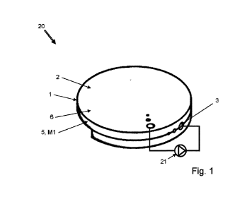
surface,
to deposit or plate materials onto the surface, or to electrochemically etch a
stencilled design into the surface. The process requires that an electrical
circuit is
completed in the presence of a conductive fluid, which means that the
conductive
surface must be electrically connected to both of the opposing terminals of an
electrical power source. These connections are typically made through the use
of
a pair of opposing electrodes ¨ for convenience, these will be referred to
hereafter
as the 'work' electrode and a 'return' electrode to denote that the electrodes
are
connected to opposing power source terminals. The electrochemical processes
require that the work electrode is either positively or negatively charged
relative
to the conductive surface and return electrode. The particular charge of the
work
electrode will depend upon the nature of the conductive surface, the desired
electrochemical process and the conductive fluid.
[0004] It is well known that, if conductive fluid is present at both the work
and
return electrodes, then opposing electrochemical reactions will occur proximal
to
both electrodes ¨ one desirable, and the other potentially undesirable.
However,
if it is desired for only one of these electrochemical reactions to occur,
then only
the work electrode should conduct electricity through the conductive fluid;
the
CA 03232066 2024-03-14
WO 2023/039641 PCT/AU2022/051126
2
return electrode should be a "direct return electrode", in that it is directly
connected to the conductive surface.
[0005] The typical prior art electrochemical cleaning/etching/marking tool
comprises a contacting implement that serves as the work electrode (sometimes
referred to as a 'wand') and conductive fluid applicator, and a grounding
clamp
that is fixed directly onto the conductive surface to provide a direct return
electrode. The contacting implement and grounding clamp are connected to
opposing terminals of a power source. So long both as the grounding clamp is
connected, touching the contacting implement along with conductive fluid to
the
conductive surface allows the circuit to complete and the desired
electrochemical
reaction to be induced.
[0006] Some alternate prior art arrangements may utilise a direct return
electrode that relies on pressure from the user and a spring in order to
maintain
a return connection to the workpiece, while others may rely on a conductive
workbench to act as a direct return electrode and maintain an electrical
connection
with the workpiece.
[0007] The skilled person will appreciate that, in general, applying or
'plating'
material onto a conductive surface requires that the work electrode is
positive with
respect to the conductive surface, while removing material (such as occurs
during
a cleaning or polishing process) generally requires that the work electrode is
negative with respect to the conductive surface. However, the skilled person
will
appreciate that the electrochemical principles are the same regardless of what
effect the user is seeking ¨ an electrical circuit must still be established,
and
conductive fluid must still be applied.
[0008] Prior art electrochemical cleaning/etching/marking tools vary in size,
shape and arrangement of work electrodes, and may carry various advantages or
disadvantages. However, each electrochemical cleaning/etching/marking tool
requires the presence of a grounding clamp or other form of direct return
electrode. Unfortunately the various prior art direct return electrode designs
each
represent significant limitations placed upon the user. For instance, use of a
grounding clamp limits the mobility of the user - the grounding clamp is
tethered
CA 03232066 2024-03-14
WO 2023/039641 PCT/AU2022/051126
3
to the electrochemical cleaning/etching tool power source via cable, and in
order
to move beyond the reach of said cable, the user must detach and re-attach the
grounding clamp in a new spot. Additionally, not all surfaces provide easy-to-
reach
protrusions that the grounding clamp may be properly attached to in order to
function; for example, large, smooth metal surfaces such as the inside of
silos or
water tanks may be devoid of suitable protrusions for receiving a grounding
clamp.
In a similar vein, spring-pressure direct return electrodes require constant
attention from the user to maintain the necessary pressure. Finally, prior art
electrochemical cleaning/etching/marking tools that rely upon conductive
workbenches limit the user in that they can only work on projects placed
directly
on the workbench ¨ such prior art tools are essentially completely immobile.
[0009] There is therefore a need to provide an electrochemical
cleaning/etching
device that provides an improvement in mobility and/or portability thereof, or
at
least overcomes some of the shortcomings of the prior art. In particular, it
is an
object of the invention to provide an electrochemical cleaning/etching device
that
does not require a separate ground clamp or other form of separate, direct-
return
electrode that tethers the user to a particular area or otherwise restricts
them.
DISCLOSURE OF THE INVENTION
[0010] In a first aspect, the present invention relates to a device comprising
a
device casing and a first and second flexible contact extending from the
casing,
each comprising a mounting means and a flexible applicator portion extending
therefrom, wherein the first and second flexible contacts are each adapted to
receive conductive fluid and subsequently to apply the conductive fluid to a
surface, and one of the first and second flexible contacts is positively
charged, and
the other is negatively charged, relative to one another.
[0011] In an embodiment, power received by the first and second flexible
contacts from the power source may be alternating current (AC) power, such
that
the first flexible contact alternates between being positively and negatively
charged, and the second flexible contact alternates between being negatively
and
positively charged, said alternating of each of the first and second flexible
contacts
occurring simultaneously and in opposing directions.
CA 03232066 2024-03-14
WO 2023/039641 PCT/AU2022/051126
4
[0012] In an embodiment, the power source may be an alternating current (AC)
power source.
[0013] In an alternate embodiment, the power source may be a direct current
(DC) power source, and the device may further comprise a switch unit between
the power source and the first and second flexible contacts, the switch unit
being
electrically connected to a voltage-out terminal, a ground terminal, and the
first
and second flexible contacts, and a switch controller connected to the switch
unit
and having a charge polarity period, the switch unit has a first configuration
wherein the first flexible contact is positively charged, and the second
flexible
contact is negatively charged relative to one another, and a second
configuration
wherein the first flexible contact is negatively charged, and the second
flexible
contact is positively charged relative to one another, and the switch
controller is
configured to periodically toggle the switch unit between the first and second
configurations at a rate determined by the toggle period.
[0014] In an embodiment, the device may further comprise a DC-DC converter
electrically connected to the power source and the switch unit, the voltage-
out
terminal and the ground terminal are respective terminals of the DC-DC
converter,
and the DC-DC converter is configured to: receive a constant voltage input
from
the power source, convert the constant voltage input into a pulsing voltage
output,
and provide the pulsing voltage output to the switch unit via the voltage-out
terminal, further wherein the pulsing voltage output comprises a voltage
waveform having a repeating pattern formed by alternating maximum and
minimum voltages and having a pulse period, and the charge polarity period is
substantially equal to an integer multiple of the pulse period. In an
embodiment,
the charge polarity period may be substantially equal to an odd integer
multiple
of the pulse period.
[0015] In an embodiment, the pulsing voltage output may comprise a voltage
waveform having an asymptotic slope at minimum voltages thereof and otherwise
having a non-asymptotic slope, and a timing of the switch unit being toggled
by
the switch controller is substantially aligned with the minimum voltages. In
an
embodiment, the voltage waveform may be a rectified full-wave sine waveform.
CA 03232066 2024-03-14
WO 2023/039641 PCT/AU2022/051126
[0016] In an embodiment, the switch unit may comprise an array of switches,
the array comprising: a first switch forming a closable circuit segment
between
the voltage-out terminal and the first flexible contact, a second switch
forming a
closable circuit segment between the voltage-out terminal and the second
flexible
contact, a third switch forming a closable circuit segment between the ground
terminal and the first flexible contact, and a fourth switch forming a
closable circuit
segment between the ground terminal and the second flexible contact, further
wherein toggling the switch unit to the first configuration comprises closing
the
first and fourth switches and opening the second and third switches, and
toggling
the switch unit to the second configuration comprises opening the first and
fourth
switches and closing the second and third switches.
[0017] In an alternate embodiment wherein the power source is a direct current
(DC) power source, the first flexible contact may comprise a contacting area
substantially smaller than a contacting area of the second flexible contact.
In an
embodiment, the contacting area of the first flexible contact may be at least
two
times smaller than the contacting area of the second flexible contact.
[0018] In an embodiment, the DC power source may be a battery, power cell,
fuel cell or other self-contained DC power source.
[0019] In an embodiment, at least one of the first and second flexible
contacts
may comprise a roller having a roller mount and a rolling element formed of an
absorbent material mounted to the roller mount, the rolling element being
adapted
to receive the conductive fluid and subsequently to apply the conductive fluid
to
the surface.
[0020] In an embodiment, the roller may be a split roller having a first
rolling
element portion arranged to form the first electrode and a second rolling
element
portion arranged to form the second electrode, the split roller is
electrically
connected to the power source, and the first and second rolling element
portions
are electrically isolated from one another.
CA 03232066 2024-03-14
WO 2023/039641 PCT/AU2022/051126
6
[0021] In an embodiment, at least one of the first and second flexible
contacts
may comprise an absorbent pad adapted to receive the conductive fluid and
subsequently to apply the conductive fluid to the surface.
[0022] In an embodiment, at least one of the first and second flexible
contacts
may comprise a brush. In an embodiment, the brush may comprise conductive
filam ents.
[0023] In an embodiment, the device may further comprise a partitioning
element formed of non-conductive material arranged to prevent the first or
second
flexible contact directly contacting the other flexible contact. In an
embodiment,
the partitioning element may comprise a shroud that at least partially extends
around at least one of the first and second flexible contacts.
[0024] In an embodiment, the power source may be an on-board power source
contained within or mounted to the device casing. In an embodiment, the on-
board power source may be within a power source housing that is detachably
mounted to the device casing.
[0025] In an alternate embodiment, the power source may be in a power source
housing that is spaced apart from and electrically connected to the device
casing.
[0026] In an embodiment, the device may further comprise a fluid conduit
arranged to provide the conductive fluid from a fluid source to each of the
first
and second flexible contacts. In an embodiment, the fluid source may be a
fluid
reservoir contained within or mounted to the device casing. In an embodiment,
the fluid reservoir may be detachable from the device casing. In an embodiment
wherein the power source is in a power source housing that is detachably
mounted
to the device casing, the fluid reservoir may be located within the power
source
housing.
[0027] An embodiment of the device, when used to electrolytically clean and
passivate a weld in the conductive article. An embodiment of the device, when
used to electrochemically etch a design, pattern or other form of marking into
a
surface of the conductive article.
CA 03232066 2024-03-14
WO 2023/039641 PCT/AU2022/051126
7
[0028] Further embodiments or variations of the invention may be disclosed
herein or may otherwise become apparent to the person skilled in the art
through
the following disclosure. These and other embodiments are considered to fall
within the scope of the invention.
DESCRI PTI ON OF FIGURES
[0029] Embodiments of the present invention will now be described in relation
to figures, wherein:
Figures 1A & 1B depict an embodiment of the invention;
Figure 2 depicts desired and undesired reactions;
Figures 3-5 are circuit diagrams for alternate embodiments of the invention;
Figures 6A-60 are Voltage Waveform graphs for an embodiment of the invention;
Figures 7 & 8 are circuit diagrams for embodiments of the invention comprising
switch units;
Figures 9A-100 are Voltage Waveform graphs for embodiments of the invention
comprising switch units;
Figures 11A & 11B depict alternate embodiments of the invention; and
Figures 12-16 depict various embodiments of the first and/or second flexible
contacts.
DETAI LED DESCRI PTI ON OF PREFERRED EMBODI MENTS
[0030] In a first aspect, the present invention relates to a device for
applying a
conductive fluid to a conductive surface, so as to clean, passivate, etch or
otherwise treat the conductive surface. Figures 1A & 1B depict an embodiment
of
the invention, wherein Figure 1A is a visual depiction thereof and Figure 1B
is a
circuit diagram thereof. The depicted embodiment of the device comprises a
device casing 10, and a first and second flexible contact 14,16 extending from
the
device casing. The first and second flexible contacts 14,16 are in electrical
communication with opposing terminals of a power source 12 (said electrical
connection is depicted by the dot-and-dash line in Figure 1A), such that one
of the
flexible contacts will be positively charged and the other will be negatively
charged, relative to one other, and are each configured to be able to carry
conductive fluid in some manner. The first and second flexible contacts 14,16
may
CA 03232066 2024-03-14
WO 2023/039641 PCT/AU2022/051126
8
comprise a mounting means for affixing said flexible contact to the device
casing
10, and a flexible applicator portion configured to carry the conductive
fluid.
[0031] As used herein, the term 'charge polarity' refers to whether an element
is positively or negatively charged. As used herein and unless otherwise
explicitly
specified, identification of the charge polarity of either flexible contact
14,16
should be interpreted as identification relative to the other flexible
contact. For
example, if the first flexible contact is positively charged and the second
flexible
contact is grounded, the second flexible contact is 'negatively charged'
relative to
the first flexible contact.
[0032] As the circuitry diagram of Figure 1B shows, there is no direct
electrical
connection between the first and second flexible contacts 14,16. Upon applying
the conductive fluid to a conductive surface 18 with the first and second
flexible
contacts 14,16, an electrical circuit is completed through the conductive
surface,
such that a voltage generated by power source 12 causes an electric current to
flow between the first and second flexible contacts through the conductive
surface
18 (and any conductive fluid that may be present). The power source 12 may be
any particular power source that is capable of providing a sufficient voltage.
The
power source 12 is depicted in Figure 1A as a portable battery pack, but this
is
exemplary only.
[0033] As the skilled person will appreciate, electrochemical processes such
as
weld cleaning, surface passivation and electrochemical etching or marking all
require that a particular conductive fluid is present and that a circuit be
formed to
enable electricity to flow, thereby driving the electrochemical reactions
between
the ions dissolved in the conductive fluid and the conductive surface 18. As
the
device comprises oppositely-charged first and second flexible contacts 14,16,
both
of which are adapted to be able to carry conductive fluid, then either
flexible
contact is able to serve as both a 'work electrode' and a 'return electrode',
depending upon the desired electrochemical reaction and the relative charges
of
the flexible contacts. This may be contrasted to prior art arrangements that
utilise
a grounding clamp or spring mechanism, which are unable to act as 'work
electrodes' due to being unable to carry or apply the conductive fluid and
connect
CA 03232066 2024-03-14
WO 2023/039641 PCT/AU2022/051126
9
directly to the conductive surface 18, limiting the flow of electrical current
through
any conductive fluid that may be present proximal thereto.
[0034] In at least one embodiment of the invention there may be multiple first
flexible contacts 14 electrically arranged in parallel to one another, and/or
multiple
second flexible contacts 16 electrically arranged in parallel to one another.
These
embodiments are not considered to be a departure from the scope of the
invention, and any reference to one first or second flexible contact 14,16
should
be considered to be equally applicable to multiple first or second flexible
contacts
unless otherwise specified.
[0035] It is considered that embodiments of the present invention may enable a
user to electrolytically clean and passivate a weld, electrochemically etch a
design,
pattern or other form of marking on a conductive surface of an article,
without
the need for a grounding clamp, grounding spring mechanism or conductive
workbench. This may enable the user to use the device with substantially
improved mobility and flexibility compared to a prior art tool that requires a
grounding clamp and thus is tethered in place. The user may also be able to
use
an embodiment of the device on ladders, in a harness, or in other difficult-to-
access or restricted-movement situations, without the risk of the grounding
clamp
and cable fouling their movement.
[0036] The skilled person will appreciate that electrochemical processes
require
a particular voltage potential in order to occur at a useful rate. In at least
one
embodiment, the power source 12 may be a power source capable of providing at
least 12 volts. In a further embodiment, the power source 12 may provide at
least
18 volts.
Desired and Undesired Reactions
[0037] With reference to Figure 2, depicted is a portion of an embodiment of
the
present invention arranged for use in cleaning or polishing a conductive
surface.
Shown are the first and second flexible contacts 14,16 the conductive surface
18,
comprising bulk material 18A and a surface layer 18B on top, and the
conductive
fluid 20. In some embodiments, the surface layer 18B may be oxidised material,
CA 03232066 2024-03-14
WO 2023/039641 PCT/AU2022/051126
weld tint or other depositions on the conductive surface 18 and thus covering
the
bulk material 18A. In other embodiments (not depicted), the surface layer 18B
may be an upper layer of the conductive surface 18 that is being removed to
expose the underlying bulk material 18A, such as through an etching process.
Although not depicted, the person skilled in the art will appreciate that the
flexible
contacts are oppositely charged relative to one another, and that the
appropriate
charge polarity for the desired reaction will depend upon the nature of the
conductive surface, the particular electrochemical process being applied
thereto,
and the type of conductive fluid being employed. For simplicity of
explanation, the
flexible contact 14,16 that is appropriately charged to promote the desired
reaction 22 may be referred to herein as the "active flexible contact".
[0038] As both the first and second flexible contacts 14,16 are in contact
with
conductive fluid, a reaction process 22, 24 takes place at each flexible
contact.
The reaction process that occurs at each flexible contact depends on the
charge
polarity thereof with respect to the conductive surface and the other flexible
contact, the natures of which are well known in the art. Positively-charged
ions in
solution within the conductive fluid will migrate away from the positively
charged
flexible contact, through the conductive fluid and towards the conductive
surface
and the negatively charged flexible contact. Similarly, negatively-charged
ions in
solution will migrate away from the negatively-charged flexible contact and
towards the positively-charged flexible contact and the conductive surface.
[0039] Generally, only one of these processes will be the desired process 22 ¨
which is depicted in example Figure 2 as surface layer 18B entering solution
within
the conductive fluid 20, migrating towards the appropriately-charged first
flexible
contact 14, and ultimately depositing thereupon. Charge-balancing processes 24
may comprise other reactions such as gas or water evolution, which are non-
detrimental, but may also comprise the reverse of the desired process 22. For
example, as depicted by the curved arrows, charge-balancing process 24 may
also comprise re-deposition of material drawn into solution from surface layer
18B
back onto the conductive surface 18, which is undesirable. Undesirable forms
of
the charge-balancing process 24 may also comprise dissolution of material
deposited upon the second flexible contact 16, movement of these ions to the
conductive surface 18, and subsequent deposition thereupon.
CA 03232066 2024-03-14
WO 2023/039641 PCT/AU2022/051126
11
[0040] The person skilled in the art will appreciate that the nature of the
conductive surface 18 (including the natures of the bulk material 18A and
surface
layer 18B), the conductive fluid 20 and the desired and undesired processes
22,24
may vary between applications of an embodiment of the invention. The skilled
person will further appreciate that these various natures are, in general,
well
known in the art.
Desired Process Promotion/Undesired Process Amelioration
[0041] The time it takes for an electrochemical reaction to occur at the
respective reaction sites depends on the velocity of movement of the ions in
solution and the length of the path the ion needs to travel. The ion velocity
depends on the nature of the ion, concentration of the solution, the
temperature,
and the applied potential gradient. With further reference to Figure 2 and
without
limiting the scope of the invention through theory, it is considered that when
the
desired process 22 comprises dissolution of surface material (such as through
etching, cleaning and/or polishing), the 'path length' of the desired process
22 is
the distance between the first flexible contact 14 and the surface layer 18B
immediately proximal thereto.
[0042] Conversely, one form of the undesired process (being represented by the
curved arrows in charge-balancing process 24) requires that dissolved ions of
the
surface layer 18B first migrate through the conductive fluid 20 over towards
the
second flexible contact 16, and only then can they subsequently migrate to the
conductive surface 18 for deposition thereupon, as the dissolved ions must
first
leave the influence of the first flexible contact 14. An alternate form of the
undesired process (dissolution of material that is on the second flexible
contact 16
and subsequent deposition upon the conductive surface 18) requires three
steps:
dissolution, migration and deposition. It has been found that, in general, the
undesired process takes longer to complete as the desired process 22 does. In
some embodiments, the undesired process may take at least twice as long as the
desired process.
CA 03232066 2024-03-14
WO 2023/039641
PCT/AU2022/051126
12
[0043] In arrangements (not depicted) wherein the desired process 22 is
marking through deposition or plating of material onto the conductive surface,
the
desired process 22 draws upon ions that are already dissolved in the
conductive
fluid 20. Ions move away from the appropriately-charged flexible contact and
towards the conductive surface 18 as well as the oppositely-charged other
flexible
contact. Deposition of the ions upon the other flexible contact, or drawing of
the
material deposited on the conductive surface 18 back into solution, are
typically
undesired processes. As with the example discussed previously, it is envisaged
that completion of the undesired process (movement of ions from, e.g., the
first
flexible contact 14 or the conductive surface 18 to the second flexible
contact 16
and subsequent deposition thereupon) takes longer to complete than the desired
process 22.
[0044] Based upon the above, a particular electrochemical process (i.e. the
desired process 22 and its related charge-balancing and/or undesired process
24),
applied to a conductive surface 18 having a particular nature and utilising a
particular conductive fluid 20 and applied voltage, will have a particular
Desired
Process Completion Time (Tc) that obeys the following equation:
Tarnin < Tu
Wherein TD,min is the minimum time required for the desired process 22 to
proceed,
while Tu is the time required for the undesired process 24 to proceed. The
skilled
person will appreciate that Tc is a range of time values between TD,min and
Tu.
[0045] In an embodiment, promotion of the desired reaction 22 and limitation
of the charge-balancing reaction(s) 24 may be able to be achieved by rapidly
switching the charge polarity of the first and second flexible contacts 14,16,
such
that they will alternate between being positively or negatively charged
relative to
one another. Without limiting the scope of the invention through theory, it is
envisaged that by switching the charge polarities of the first and second
flexible
contacts 14,16 such that each unbroken period of time spent with a particular
charge polarity is greater than the minimum time required for the desired
process,
but less than the time required for the undesired process, then the desired
process
22 may be selectively promoted over the undesired process, thereby reducing,
CA 03232066 2024-03-14
WO 2023/039641 PCT/AU2022/051126
13
negating or at least ameliorating the need for a direct-return electrode such
as a
ground clamp.
[0046] With respect to cleaning, etching or polishing arrangements, for ease
of
explanation it will be described in terms of an arrangement wherein the
surface
layer 18B dissolves to form positively-charged ions ¨ such as when the surface
layer being removed comprises a metal. The device is powered such that the
first
flexible contact 14 is negatively charged, while the second flexible contact
16 is
positively charged. Surface layer 18B is drawn into solution and ions thereof
migrate towards the first flexible contact 14, with a portion migrating across
the
conductive fluid 20, leaving the influence of the first flexible contact 14
and
subsequently becoming influenced by the positively-charged second flexible
contact. However, before these ions may be re-deposited, the charge polarity
of
the power source 12 is reversed, such that the first flexible contact 14 is
now
positively charged and the second flexible contact 16 is negatively charged.
[0047] With respect to marking or electroplating arrangements, by way of
explanatory example the device may be powered such that the first flexible
contact
14 is positively charged, while the second flexible contact 16 is negatively
charged.
Positively-charged ions that are already dissolved in the conductive fluid 20
are
urged by the positively-charged first flexible contact 14 to deposit upon the
conductive surface 18 as well as to migrate from the first flexible contact
towards
the second flexible contact 16. However, by reversing the charge polarity of
the
flexible contacts 14,16 before the ions can plate thereupon, plating or
depositing
of the dissolved material upon the now-positively charged second flexible
contact
16 is reduced, inhibited or at least ameliorated.
[0048] Although the above examples are described with reference to positively-
charged ions being drawn into or deposited out of solution, the skilled person
will
appreciate that this is exemplary only and that adapting the device for
drawing or
depositing negatively-charged ions into or out of solution is within the scope
of
the invention as disclosed herein.
[0049] In a further embodiment, the device may be configured such that a
voltage at the first flexible contact 14 when the first flexible contact is
positively
CA 03232066 2024-03-14
WO 2023/039641 PCT/AU2022/051126
14
charged, and a voltage at the second flexible contact 16 when the second
flexible
contact is positively charged, are substantially similar in magnitude to one
another. In an alternate further embodiment, the device may be configured such
that a voltage at the first flexible contact 14 when the first flexible
contact is
negatively charged, and a voltage at the second flexible contact 16 when the
second flexible contact is negatively charged, are substantially similar in
magnitude to one another. In either embodiment, the device may be further
configured such that each of the flexible contacts 14,16 spends substantially
similar time positively or negatively charged, so as to inhibit or at least
ameliorate
any 'DC bias' that may occur.
[0050] The unbroken period of time spent charged to a particular charge
polarity
may be referred to herein as a 'charge polarity period' (Tp) ¨ i.e., the
period of
time between the flexible contacts 14,16 switching charge polarity. In an
ideal
embodiment, the charge polarity period Tp is equal to the Desired Process
Completion Time Tc.
[0051] In an alternate embodiment, the first flexible contact 14 may be
configured to promote the desired reaction 22 by comprising a decreased
contact
area compared to the second flexible contact 16. As the skilled person will
appreciate, while the overall rates of reaction of each of the desired
reaction 22
and charge-balancing reaction(s) 24 are at least partially dependent upon the
total
current flowing through the completed circuit, the rate the desired reaction
22 or
charge-balancing reaction(s) 24 per unit area is dependent upon current
density.
As such, by decreasing a contact area of the first flexible contact 14 to be
substantially smaller than a contact area of the second flexible contact 16,
such
that the current density immediately proximal to the first flexible contact 14
is
increased relative to the current density immediately proximal to the second
flexible contact 16, thereby increasing the rate of the desired reaction 22
per unit
area. Conversely, any product of the charge-balancing reaction(s) 24 will be
spread over a relatively greater surface area without an increase in quantity
produced, allowing any undesired depositions to be gradually thinned out and
substantially removed. In a further embodiment, the contact area of the first
flexible contact 14 may be at least two times that of the second flexible
contact
16. The skilled person will appreciate that the ratio between the contact
areas of
CA 03232066 2024-03-14
WO 2023/039641 PCT/AU2022/051126
the first and second flexible contacts 14,16 may also be dependent upon
various
factors, such as the reaction rate per unit area of the desired and undesired
reactions 22,24.
Power Sources
[0052] In one embodiment and with reference to Figure 3, switching of the
charge polarity of the first and second flexible contacts 14,16 may be enabled
by
utilising an alternating current (AC) power source 12A. It is considered that
AC
power sources offer a benefit in that promotion of the desired reaction 22
through
charge polarity switching may be achieved without requiring complex electrical
circuitry. As the skilled person will appreciate, an AC power source 12A will
have
an associated power output frequency, the inverse of which will be the power
output period (Toutput). The power output period is equal to the length of
time that
it takes for a particular flexible contact 14,16 to completely cycle through
charge
polarities, e.g. the time from being positively charged to negatively charged
and
back again, and therefore the power output period Toutput is double the charge
period Tp. As such, in a further embodiment the AC power source 12A may be
selected or configured such that its power output is of a frequency (f) that
obeys
the following criterion:
1
-= Toutput = 2 X Tp = 2 X 1',
[0053] AC power sources are not always practical, especially where portability
is
desired. As such, in an alternate embodiment of the present invention and with
reference to Figure 4, the power source 12 may be a direct current (DC) power
source 12B. It is considered that the use of a DC power source 12B may be
particularly beneficial in providing an embodiment of the device that is
portable.
In some embodiments, the DC power source 12B may be one or more of a fuel
cell, a battery, a power cell, or an alternate form of a self-contained DC
power
source.
[0054] Embodiments of the invention utilising a DC power source 12B may be
able to be configured to promote the desired reaction 22 by decreasing the
contact
area of the first flexible contact 14.
CA 03232066 2024-03-14
WO 2023/039641 PCT/AU2022/051126
16
Charge Polarity Switching with DC Power Source
[0055] DC power sources 12B are not natively capable of enabling promotion of
the desired reaction 22 through charge polarity-switching. Therefore, in order
to
enable this functionality without sacrificing the potential portability
offered by a
DC power source 18B such as a fuel cell or battery pack, in an alternate
further
embodiment and with reference to Figure 5, the device may further comprise a
switch unit 26 between the DC power source 12B and the flexible contacts
14,16,
and a switch controller 28 connected to the switch unit. The switch unit may
be
electrically connected to a voltage-out terminal 30, a ground terminal 32, and
the
first and second flexible contacts 14,16. In such an embodiment, the switch
unit
26 may have a first configuration wherein the first flexible contact 14 is
positively
charged and the second flexible contact 16 is negatively charged, and a second
configuration wherein the first flexible contact is negatively charged and the
second flexible contact is positively charged. The switch controller 28 may be
configured to periodically toggle the switch unit 26 between the first and
second
configurations according to the charge polarity period Tp, such that Tp = Tc.
[0056] In some embodiments, the switch controller 28 may toggle the switch
unit 26 by periodically emitting a single 'toggle' signal. In such an
embodiment,
the charge polarity period may be equal to the 'clock period' of the switch
controller 28, being the period of time between signal pulses. In some
alternate
embodiments, the switch controller 28 may toggle the switch unit 26 by
alternately
emitting two different signals, being a 'toggle from first configuration to
second'
signal and a 'toggle from second configuration to first' signal. As the
skilled person
will appreciate, in such an embodiment the 'clock period' of the switch
controller
would be the period of time between two sequential instances of the same
signal
(e.g. two sequential instances of emitting a 'toggle from first configuration
to
second' signal) and would therefore be twice the length of the charge polarity
period.
[0057] In an embodiment of the invention comprising a switch unit 26 and
switch
controller 28, the first and second flexible contacts 14,16 may have
respective
contact areas that are substantially similar in size, so as to ameliorate or
otherwise
inhibit the inducement of DC voltage bias during use of the device. In the
CA 03232066 2024-03-14
WO 2023/039641 PCT/AU2022/051126
17
embodiment depicted in Figure 5, the voltage-out terminal 30 and ground
terminal
32 are depicted as respective terminals of the DC power source 126, however
the
skilled person will appreciate that other circuitry components may be
positioned
between the DC power source 126 and the switch unit 26. As used herein, the
terms voltage-out terminal 30 and/or ground terminal 32 may refer to the
respective terminals immediately 'upstream' or 'downstream' of the switch unit
26
(depending on whether the other circuit component is providing the voltage-out
terminal 30 and/or ground terminal 32).
[0058] Figure 6a depicts the electrode potential at the first flexible contact
14,
while Figure 6b depicts the electrode potential at the second flexible contact
16,
when a switch unit 26 is implemented, for an 18-volt DC power source 126 and
assuming no loss. Finally, Figure 6c depicts the voltage across both flexible
contacts 14,16. Although the overall voltage waveform is rendered such that
the
first flexible contact 14 is the default 'positive' terminal, the skilled
person will
appreciate that this is convention only and does not limit the scope of the
invention. As the skilled person may appreciate, the 'peak-to-peak' voltage
across
both contacts is 36 volts, double the voltage of the 18-volt DC power source
126.
[0059] In an embodiment and with reference to Figure 7, the switch unit 26 may
comprise an array of switches, having at least a first switch 26A, a second
switch
266, a third switch 260 and a fourth switch 26D. The first switch 26A may form
a
closable circuit segment between the voltage-out terminal 30 and the first
flexible
contact 14, the second switch 266 may form a closable circuit segment between
the voltage-out terminal 30 and the second flexible contact 16, the third
switch
260 may form a closable circuit segment between the first flexible contact and
the
ground terminal 32, and the fourth switch 26D may form a closable circuit
segment
between the second flexible contact and the ground terminal. In such an
embodiment, the switch controller 28 may be configured such that toggling the
switch unit 26 to the first configuration comprises closing the first and
fourth
switches 26A,26D and opening the second and third switches 266,260, and
toggling the switch unit to the second configuration comprises opening the
first
and fourth switches 26A,26D and closing the second and third switches 266,260,
wherein a closed switch enables electricity to flow therethrough and an open
switch inhibits the flow of electricity therethrough.
CA 03232066 2024-03-14
WO 2023/039641 PCT/AU2022/051126
18
[0060] One or more of the switches 26A-D may comprise a transistor. One or
more of the switches 26A-D may comprise a thyristor and diode connected in
parallel. In an embodiment, the switch unit 26 may comprise a full-bridge
inverter
switch.
Interference Mitigation
[0061] In at least one embodiment of the invention comprising a switch unit
26,
the electrode potential at each of the first and second flexible contacts
14,16 may
be a square waveform. An example of each waveform is shown in Figures 6a and
6b, in which the switch controller 28 toggles the switch unit 26 between the
first
and second configurations every two milliseconds (i.e., Tp = 2m5). The skilled
person will appreciate that the voltage and charge polarity period are
selected
arbitrarily and for example purposes only. When toggling at high frequencies,
the
rapid spike or dip in voltage that occurs at the edge of each 'square' in the
waveforms depicted in Figures 6a-c can induce high levels of electromagnetic
interference in nearby electrical circuits and other electronics, wherein the
amount
of generated electromagnetic interference is at least partially proportional
to the
instantaneous rate of change in voltage. While an embodiment of the present
invention that produces electromagnetic interference may be suitable in some
situations, it may not be adequate when the device is being used, for example,
in
areas with sensitive electronics.
[0062] In order to ameliorate this, an embodiment of the device may be
configured to reduce the voltage across the first and second flexible contacts
when
the switch unit 26 is to be toggled, so that the instantaneous rate of change
of
voltage across the first and second flexible contacts 14,16 caused by the
toggling
of the switch unit 26 is reduced, thereby reducing or ameliorating the amount
of
generated electromagnetic interference.
[0063] In an embodiment and with reference to Figure 8, the device may further
comprise a DC-DC converter 34 between the DC power source 12B and the switch
unit 26. In at least the present embodiment, the voltage-out terminal 30 and
ground terminal 32 that electrically connect to the switch unit 26 are
respective
CA 03232066 2024-03-14
WO 2023/039641 PCT/AU2022/051126
19
terminals of the DC-DC converter. In at least the present embodiment, the DC-
DC converter 34 may be configured to receive a constant voltage input from the
DC power source 12B, convert the constant DC voltage input into a pulsing DC
voltage output, and provide the pulsing DC voltage output to the switch unit
26
via the voltage-out terminal 30. The skilled person will appreciate that the
DC-DC
converter 34 is not producing AC output.
[0064] In a further preferred embodiment, the pulsing voltage output comprises
a voltage waveform having a repeating pattern formed by alternating maximum
and minimum voltages and having a pulse period (Tp ) As used herein, the term
ulse, =
'pulse period' refers to the period of time that it takes for the pulsing
voltage
output to repeat ¨ for example, the length of time between two sequential
maximum voltages, or two sequential minimum voltages.
[0065] In a further preferred embodiment, the pulsing voltage output may
comprise a voltage waveform that has an asymptotic slope at minimum voltages
and otherwise has a non-asymptotic slope, such that the voltage waveform is
substantially curved at non-minimum values of the voltage. An example of a
waveform having asymptotic slope at minimum voltages and otherwise a non-
asymptotic slope is depicted in Figure 9A, wherein the pulse period Tpuise of
the
depicted waveform is 2 ms. While the voltage waveform depicted in Figure 9A
comprises a minimum voltage of OV, this is selected for example purposes only.
The minimum voltage may be selected as a value above OV, such as the voltage
waveform of an alternate embodiment of a pulsing voltage output as depicted in
Figure 9B. The skilled person will appreciate that the voltages and pulse
periods
depicted in Figures 9A and 9B are for example purposes only.
[0066] In an embodiment, the charge polarity period Tp of the switch
controller
28 is configured to be substantially equivalent to an integer multiple of
pulse
periods Tpuise= In a further embodiment, the integer multiple of pulse periods
an
odd integer multiple. In a further embodiment, the odd integer multiple of
pulse
periods may be one, i.e., the charge polarity period Tp may be substantially
equal
to the pulse period Tpuise=
CA 03232066 2024-03-14
WO 2023/039641 PCT/AU2022/051126
[0067] In an embodiment, a timing of the switch unit 26 being toggled by the
switch controller 28 may be substantially aligned with the minimum voltages so
as to reduce the level of generated electromagnetic interference. As the
voltage
across the first and second flexible contacts 14,16 is substantially reduced,
upon
inversion of charge polarity of said flexible contacts, the instantaneous rate
of
change of voltage will be significantly lowered. In a further embodiment, if
the
minimum voltage is at or near zero, so as to substantially entirely ameliorate
the
generation of electromagnetic interference.
[0068] Figures 10A and 10B depict the voltage waveforms for the first flexible
contact 14 and the second flexible contact 16, where the potential is measured
as
a voltage between the respective flexible contact 14,16 and the conductive
surface
18, while Figure 100 depicts the voltage waveform of the device across the
flexible
contacts 14,16, based upon an example 18-volt DC power source 12B input. In
Figure 100, the overall voltage waveform is rendered such that the first
flexible
contact 14 is the default 'positive' terminal, but the skilled person will
appreciate
that this is convention only and does not limit the scope of the invention.
[0069] Contrasting Figure 6C to 100, the skilled person may appreciate that
the
instantaneous rate of change of voltage is substantially reduced at each
instance
of toggling, and as a result generation of electromagnetic interference may be
substantially ameliorated. Rather than the voltage across the first and second
flexible contacts 14,16 suddenly changing, the transition is smoothed out into
a
sinusoidal shape. This may be in addition to the reduction of generated
electromagnetic interference achieved by reducing the voltage across the first
and
second flexible contacts 14,16 immediately prior to toggling the charge
polarity
thereof.
[0070] As the skilled person may appreciate, the peak voltage values in Figure
10a and 10b are essentially identical to the voltage output of the DC power
source
12B, such that the peak-to-peak voltage (based upon an 18-volt DC power source
12B input) is 36 volts. In the case of a voltage waveform substantially
approaching
a sine wave, the 'useful' voltage - being the RMS voltage - will be
approximately
12.6 volts (18V*1N2). It is considered that an embodiment of the device may
thus be able to be compatible or usable with a typical 18V power tool battery
pack,
CA 03232066 2024-03-14
WO 2023/039641 PCT/AU2022/051126
21
while still producing a high enough voltage and sufficient current to drive a
desired
electrochemical reaction at a useful rate.
Power and Fluid Source Design
[0071] In an embodiment and with reference to Figure 11A, the power source
12 may be on-board power source 36. In such an embodiment, the device may
be a fully-portable device. In a further embodiment, the on-board power source
36 may be within a power source housing 38 that is detachable from a handle
portion 40 of the device from which the first and second flexible contacts
14,16
extend.
[0072] In an alternate embodiment and with reference to Figure 11B, the power
source 12 may be in a power source housing 38 that is spaced apart from and
electrically connected to a handle portion 40 of the device from which the
first and
second flexible contacts 14,16 extend. The power source housing 38 may be
electrically connected to the handle portion of the device by one or more
flexible
cables. Such an embodiment may enable use of the device for extended periods
of time.
[0073] In an embodiment, the device may further comprise a fluid conduit 42
that is arranged to deliver the conductive fluid, from a fluid source 44, to
at least
one of the first and second flexible contacts 14,16. This may enable at least
partially-continuous flow of the conductive fluid to the first and second
flexible
contacts 14,16, removing or at least ameliorating a need to dip the first and
second flexible contacts in a container of said conductive fluid. Delivery of
conductive fluid through the fluid conduit 42 may be manual (e.g. actuated by
a
user-operated button or switch), or may be automatic. Delivery may be pressure
driven, such as by one or more pump units. In a further embodiment, the fluid
source may be a fluid reservoir 46 contained within or mounted to the device
casing 10 and in fluid communication with the fluid conduit 42. In a further
embodiment (not shown) wherein the device also comprises the power source 12
within a power source housing 38, the fluid reservoir 46 may be located within
the
power source housing.
CA 03232066 2024-03-14
WO 2023/039641 PCT/AU2022/051126
22
Flexible Contact Design
[0074] In general and with reference to Figure 12, the first and second
flexible
contacts each comprise a mounting means 48 for mounting to the device casing
and receiving electrical current from the power source 12, and a flexible
applicator portion 50 extending therefrom that is adapted to apply conductive
fluid
to the conductive surface 18. The first and second flexible contacts 14,16 are
further adapted so that electrical current can run from the power source 12,
through the respective flexible contact and into the conductive fluid. In some
embodiments, this may be achieved by a conductive element contacting or
protruding into the flexible applicator portion 50, and thus into contact with
the
conductive fluid carried therein. In alternate embodiments, the flexible
applicator
portion 50 may be comprised of conductive material, thereby enabling electric
current to travel therealong, either alongside or instead of electrical
current
travelling through the loaded conductive fluid. In some embodiments, the
mounting means 48 may be adapted to receive conductive fluid through a fluid
conduit 46.
[0075] With further reference to Figure 12, in an embodiment the flexible
applicator portion 50 may comprise an absorbent pad 50A on the end of the
mounting means 48. The embodiment may also comprise a conductive element
52. The absorbent material serves as the fluid-carrying means, and carries the
conductive fluid and allows its application to a conductive surface (not
shown).
[0076] In an embodiment and with reference to Figure 13, the flexible
applicator
portion 50 of at least one of the first and second flexible contacts 14,16 may
be a
roller element comprising an absorbent material and mounted onto the mounting
means 48. As with embodiments comprising an absorbent pad 50A, the absorbent
material of the roller element 50B serves to carry the conductive fluid. In a
further
embodiment and with reference to Figure 14, each of the first and second
flexible
contacts 14,16 may be provided in the form of a split roller, having a first
mounting
means 48-1 and first roller element 50B-1 arranged to form the first flexible
contact 14, and a second roller means 48-2 and second roller element 50B-2
arranged to form the second flexible contact 16. In an embodiment, the split
roller
may comprise one or more central portions 54 to provide some structural
rigidity.
CA 03232066 2024-03-14
WO 2023/039641 PCT/AU2022/051126
23
In such an embodiment, the central portion 54 is non-conductive so as to
ensure
that the first and second roller elements 50B-1,50B-2 are electrically
isolated from
one another.
[0077] In an embodiment and with reference to Figure 15, the flexible
applicator
portion 50 of at least one of the first and second flexible contacts 14,16 may
be a
brush. In a further embodiment, the flexible applicator portion 50 of the
brush
may comprise conductive filaments 500. In further embodiments, the brush may
be extendable and/or retractable. Extension and/or retraction thereof may be
manual, or may alternatively be driven by a motor. Extension and/or retraction
may be automated by a switch controller based upon input of a sensor to sense
an extent to which the brush has been worn down through use.
[0078] As the skilled person will appreciate, the flexible applicator portion
50 of
the first and second flexible contacts 14,16 are flexible. This helps to
promote
adequate and proper contact with the conductive surface 18 by both of the
contacts 14,16, which is necessary to ensure that the electrical circuit is
completed. However, depending on size, type and arrangement of the first and
second flexible contacts 14,16, the flexible contacts may be at risk of
flexing,
bending or otherwise deforming towards one another. Should they come into
direct contact with one another, the circuit may be prematurely completed and
may lead to short-circuiting. In an embodiment and with reference to Figure
16,
the device may further comprise a partitioning element 56 formed of non-
conductive material that is arranged to prevent the first or second flexible
contact
14,16 directly contacting the other flexible contact. In a further embodiment
and
with return reference to Figure 15, the partitioning element 56 may comprise a
shroud that at least partially extends around at least one of the first and
second
flexible contacts 14,16. In some embodiments, the shroud may be extendable
and/or retractable. The partitioning element 56 depicted in Figure 15 is shown
with a cut-out, but this is for explanatory and clarity purposes only.
[0079] While the invention has been described with reference to preferred
embodiments above, it will be appreciated by those skilled in the art that it
is not
limited to those embodiments, but may be embodied in many other forms,
variations and modifications other than those specifically described. The
invention
CA 03232066 2024-03-14
WO 2023/039641 PCT/AU2022/051126
24
includes all such variation and modifications. The invention also includes all
of the
steps, features, components and/or devices referred to or indicated in the
specification, individually or collectively and any and all combinations or
any two
or more of the steps or features.
[0080] In this specification, unless the context clearly indicates otherwise,
the
word "comprising" is not intended to have the exclusive meaning of the word
such
as "consisting only of", but rather has the non-exclusive meaning, in the
sense of
"including at least". The same applies, with corresponding grammatical
changes,
to other forms of the word such as "comprise", etc.
[0081] Other definitions for selected terms used herein may be found within
the
detailed description of the invention and apply throughout. Unless otherwise
defined, all other scientific and technical terms used herein have the same
meaning as commonly understood to one of ordinary skill in the art to which
the
invention belongs.
[0082] Any promises made in the present document should be understood to
relate to some embodiments of the invention, and are not intended to be
promises
made about the invention in all embodiments. Where there are promises that are
deemed to apply to all embodiments of the invention, the applicant/patentee
reserves the right to later delete them from the description and they do not
rely
on these promises for the acceptance or subsequent grant of a patent in any
country.