Note: Descriptions are shown in the official language in which they were submitted.
WO 2023/047417
PCT/1N2022/050851
LOW VOLTAGE CAPACITIVE MICROMACHINED ULTRASONIC TRANSDUCER
(CMUT) DESIGN AND MANUFACTURING FLOW
BACKGROUND
CROSS-REFERENCE TO RELATED APPLICATIONS
[0001] This application claims priority to the Indian provisional patent
application no.
202141043234 filed on September 23, 2021, the complete disclosures of which,
in their entirety,
are herein incorporated by reference.
Technical Field
[0002] The embodiments herein generally relate to a capacitive micromachined
ultrasonic
transducer (CMUT), and more particularly, to a method of designing a low
voltage capacitive
micromachined ultrasonic transducer (CMUT) for complementary
metal¨oxide¨semiconductor
(CMOS).
Description of the Related Art
[0003] A capacitive micromachined ultrasonic transducer (CMUT) is a relatively
new
concept in the field of ultrasonic transducers. Most of the commercial
ultrasonic transducers
today are based on piezoelectricity. CMUTs are the transducers where the
energy transduction is
due to a change in the stiffness coefficient of a membrane due to an
electrostatic field in a
vacuum enclosed by two conducting plates. CMUTs are constructed on silicon
using
micromachining techniques. A cavity is formed in a silicon substrate, and a
thin electrically
conducting layer suspended on the top of the cavity serves as a membrane on
which a metalized
layer acts as an electrode, together with the silicon substrate which serves
as a bottom electrode.
[0004] Existing CMUTs intended for operation whether in un-collapsed or deep-
collapse
mode require very high operating voltages of the order of 100V. Large CMUT
Arrays require a
large number of interconnects largely due to difficulties in isolating the
lower plate(s) of the
individual CMUT elements in the array. The silicon real estate used by the
array gets further
increased due to the non-availability / non-usage of a different metal layer
for the upper plate(s)
from that used by the lower plate(s), preventing Manhattan-style crossings of
interconnect lines.
Existing CMUT technologies have (at least) two constraints preventing
homogeneous integration
to bulk CMOS Processes.
1
CA 03232631 2024- 3- 21
WO 2023/047417
PCT/1N2022/050851
[0005] Accordingly, there remains a need for mitigating and/or overcoming
drawbacks
associated with current methods.
SUMMARY
[0006] In view of the foregoing, embodiments herein provide a method for
designing a low
voltage capacitive micromachined ultrasonic transducer (CMUT). The method
includes starting
from a base silicon wafer includes starting with a N-type Silicon Wafer and
growing base oxide
by performing the following steps. The method includes patterning with a metal
mask over the
base oxide. The method includes patterning with a Field Oxide (FOX) Mask over
a copper (Cu)
or Aluminium (Al) metal (M1) layer that is deposited over the base oxide. The
method includes
depositing polysilicon over the entire silicon wafer and doping the
polysilicon with a donor
species with a concentration approaching its respective solid solubility limit
and subsequently
depositing titanium (Ti) over the doped polysilicon that is deposited on the
entire silicon wafer
and subsequently depositing a dielectric layer, wherein the dielectric layer
is Silicon Dioxide or
in a stack with Hafnium Oxide or alternatively in a stack with Silicon Nitride
or a high relative
permittivity material. The method includes patterning with a pedestal¨poly
mask over a
dielectric layer that is deposited over the titanium. The method includes
removing the patterned
dielectric by a wet etch process and subsequently removing exposed titanium by
an alternative
wet etch process and sequentially excavating by reactive ion etch (R1E) all
exposed polysilicon.
The method includes planarising surface of the base silicon wafer by chemical
mechanical
polishing (CMP), thereby preparing the base silicon wafer for eventual bonding
with a separate
top silicon wafer. The method includes starting with the separate top silicon
wafer including a
silicon "device" layer on top of buried oxide grown over a thick "handle"
silicon layer and
performing the following steps. The method includes depositing by sputtering
an aluminium
layer of suitable thickness that may be referred as Metal 2. The method
includes patterning with
a Metal 2 Mask and etching the Metal 2 by a wet etch process_ The method
includes patterning
with a CMUT Cell mask and etching the silicon "device" layer by RIF to define
a CMUT top
plate. The method includes aligning the separate top silicon wafer and the
base silicon wafer to
enable the Metal 2 of the separate top silicon wafer to align with Pillar Poly
of the base silicon
wafer; and heating the separate top silicon wafer and the base silicon wafer
after the separate top
silicon wafer and the base silicon wafer are aligned to enable the Metal 2 of
the separate top
silicon wafer to (a) form a eutectic bonding between the polysilicon and
aluminium Metal 2 layer
2
CA 03232631 2024- 3- 21
WO 2023/047417
PCT/1N2022/050851
during which a certain thickness of the Metal 2 is consumed, and (b) form a
Polycide between
the Polysilicon and the Titanium (Ti) alloy in parallel, wherein the Titanium
present inside the
cavity (i) acts .... as a getter when the eutectic bonding is happening
between the polysilicon and
aluminium, (ii) forms chemical bonds with residual Nitrogen and Oxygen, and
(c) removes the
residual Nitrogen and Oxygen from the cavity, thereby improving vacuum in the
cavity. The
method includes depositing a Polymer layer over an entire wafer. The method
includes
patterning with a Polymer Mask and selectively etching the Polymer to (a)
isolate CMUT cells
from mechanical coupling and (b) remove the polymer at bond pads.
[0007] In some embodiments, the N-Type Silicon Wafer is replaced by P-Type
Silicon
Wafer. In some embodiments, concentration of the N-type Silicon Wafer is 5 x
1015/cm3,
wherein the base oxide has 0.5 vt thickness.
[0008] In some embodiments, the method includes performing dry oxidation of a
silicon
wafer to obtain a required silicon dioxide (5i02) thickness of the base
silicon wafer, the dry
oxidation is performed at 1050 C for an appropriate time interval. The
required oxide thickness
is 1pm. In some embodiments, the method includes depositing the copper (Cu) or
aluminium
(Al) metal (M1) layer with a required thickness over the base oxide (SiO2), In
some
embodiments, a thickness of the copper or Al metal 1 layer is based on a
design specification of
resistivity.
[0009] In some embodiments, the method includes etching the copper/A1 metal
using a wet
etch process to create a CMUT bottom plate and a metal (M1) interconnect layer
after the metal
mask is patterned over the base oxide; and depositing conformally 5i02 using
Plasma-Enhanced
Chemical Vapor Deposition (PECVD) over an entire silicon wafer.
[00010] In some embodiments, the method includes etching the PECVD SiO2 after
the
Field Oxide (FOX) Mask is patterned using buffer Hydrogen Fluoride (HF)
solution to obtain
CMUT cavities.
[00011] In some embodiments, the method includes etching the dielectric layer
using the
wet etch process to expose the titanium from all areas where underlying poly
is to be etched,
wherein the dielectric layer is at least one of SiO2, SiO2 / Hf02 sandwich or
SiO2 / Si3N4
sandwich.
3
CA 03232631 2024- 3- 21
WO 2023/047417
PCT/1N2022/050851
[00012] In some embodiments, the method includes etching the Titanium by the
wet-etch
process where the polysilicon acts as an "etch-stop", wherein the Titanium
(Ti) is deposited over
the polysilicon with a thickness of 100 nm by sputtering.
[00013] In some embodiments, the method includes excavating the polysilicon
inside
cavity around the pedestal and in FOX regions adjacent to pillars to prevent
shorting of adjacent
CMUTs.
[00014] In some embodiments, the Chemical Mechanical Polishing (CMP) is
performed on
the polysilicon with a thickness of 1.4 gm to remove the excess dielectric on
the pillar; and the
titanium (Ti) on pillar polysilicon and the excess height of the polysilicon
to render the surface of
a wafer planar.
[00015] In some embodiments, the method includes chemical mechanical polishing
(CMP)
of the handle silicon layer by RIE and, sequentially, a buried oxide layer by
the wet etch process.
[00016] In some embodiments, the separate top silicon wafer comprises a
heavily doped
top n+ silicon layer that is intended to be a membrane with a thickness of 2
gm. In some
embodiments, the separate top silicon wafer comprises the thick handle silicon
layer that is
removed by RIE and the buried oxide layer placed below with the thickness of
0.5 gm which is
removed by the wet-etch process with the silicon device layer acting as etch-
stop for its removal.
[00017] In some embodiments, the Metal 2 of thickness 0.8 gm is reduced to 0.4
gm
during eutectic bonding at 600 C and a 0.1 gm thick membrane dielectric leaves
a gap of 0.3
In some embodiments, different combinations of the Metal 2 thickness and
membrane dielectric
thickness are used to control gap between the membrane and the pedestal and
different sandwich
stacks to simultaneously achieve a desired capacitance value of the CMUT
independent of the
gap thickness.
[00018] In some embodiments, two plates of the CMUT embodied as the Metal 1
and the
Metal 2 are electrically isolated from corresponding plates of other CMUT
cells on a same die,
this isolation enabling compensation of stray capacitances by suitable circuit
techniques.
[00019] In some embodiments, a pedestal in one or more sizes and one or more
shapes
comprising interleaved and grid-like structures is constructed inside the
cavity of the CMUT. In
some embodiments, the pedestals enable lowering of the collapse voltage,
enable lowering of
operating voltages and improve control on a resonant frequency of vibration of
the membrane.
4
CA 03232631 2024- 3- 21
WO 2023/047417
PCT/1N2022/050851
[00020] The CMUT has an interleaved metal-insulator (silicon dioxide/silicon
nitride or
alternatively silicon dioxide / hafnium oxide sandwich) to reduce pull-in and
collapse voltage.
The CMUT includes reduced interlayer parasitic capacitance using a 2-metal
process that
surmounts a problem of stray capacitance along with increased inter-metal
dielectric breakdown.
The CMUT has low operating dc voltage and a reduced spring softening effect.
The CMUT
enables feed of dc in series with ac voltage on both plates independently.
This unlocks many
circuit techniques to be applied on the CMUT that would otherwise not be
possible. The CMUT
enables reduction of a number of interconnects when used as a two-dimensional
array. The
CMUT has a high Electric field in the cavity (between the membrane and n+
bottom plate)
increases the electro-mechanical efficiency of the CMUT.
[00021] In some embodiments, integrating getter materials in the SOT wafer
provides a
low-cost means of improving the vacuum level in the cavity, thereby increasing
gas breakdown
voltage and solving trapped gas-related problems.
[00022] The Titanium Polycide and conducting metal 1 layer below the pedestal
results in
a very simplified CMUT capacitance during Collapse. The doped Poly and the
Titanium
conducting layer ensure that the membrane characteristics and cavity gap is
controlled by the
design and properties of the Metal 2 in the top plate of the CMUT and the
dielectric thickness
within the cavity.
[00023] In some embodiments, the dielectric layer may be deposited on the
pedestal in the
bottom wafer.
[00024] In some embodiments, the dielectric layer may be on the device layer
on the top
wafer.
[00025] In some embodiments, the dielectric layer is entirely comprised of
SiO2.
[00026] In some embodiments, the dielectric layer is comprised of a sandwich
of silicon
dioxide (SiO2) arid Hafnium Oxide (Hf02).
[00027] In some embodiments, the dielectric layer is comprised of a sandwich
of silicon
dioxide (SiO2) and silicon nitride (Si3N4).
[00028] In some embodiments, a sandwich of one or more high relative
permittivity
materials may be used to faun the dielectric layer.
5
CA 03232631 2024- 3- 21
WO 2023/047417
PCT/1N2022/050851
[00029] In all embodiments, the dielectric layer results in an increased
electrical field and
increased CMUT capacitance in collapse and improved the electro-mechanical
transduction
efficiency.
[00030] The second type of CMUT also sits entirely above the silicon surface,
has a
conducting pedestal inside the cavity on the bottom wafer with a dielectric on
the bottom of the
device layer in the top wafer and may be a good fit in certain cases of post-
integration to the
Drive / Receive Electronics implemented in bulk CMOS in a Back-End Of the Line
(BEOL)
module. This can be accomplished either by using Through-Silicon-Via (TSV),
which is not a
high-yield technology yet, or by a Chip-on-Board (COB) or equivalent bonding
technique.
[00031] The third type of CMUT uses silicon dioxide below each CMUT element
for
isolation between CMUTs. Both plates of the CMUT comprise aluminium (Metal 1
and Metal
2); a dielectric layer is deposited on Metal 1 and a conducting pedestal with
or without an
interleaved structure is constructed on it. The membrane is constructed of the
silicon device layer
in a top silicon wafer and bonded to the bottom wafer by silicon to silicon
bonding.
[00032] The fourth type of the CMUT is a variant of the third type and
additionally offers
the facility to increase the fixed component of the CMUT capacitance, thereby
enabling future
scaling wherein smaller CMUT cell sizes can make interconnect parasitic become
more
significant, but a sandwich capacitor provides an answer without increasing
silicon real estate.
[00033] The CMUT and some alternative implementations of the CMUT (and by
extension
a CMUT Array comprising either cells or cell elements) can be implemented
completely on top
of a CMOS (or other) device (BEOL) with interconnections that do not require
any low yield
technology such as "through silicon yias" (TSVs).
[00034] The process steps in fabricating the CMUT are not high-cost or
equipment-centric.
The standard CMOS process steps, available in a moderately equipped foundry,
will reduce the
production cost_ The electric field and the membrane capacitance are inversely
proportional to
the effective membrane gap. The high electric field and high membrane
capacitance in the
CMUT is achieved by introducing special structures in the membrane cavity.
This reduces the
effective gap between the membrane and the bottom plate, thereby increasing an
electromechanical transduction efficiency, which is a product of electric
field and membrane
capacitance.
6
CA 03232631 2024- 3- 21
WO 2023/047417
PCT/1N2022/050851
[00035] The electromechanical transduction efficiency q=ExC (i.e., a product
of electric
field and membrane capacitance). The CMUT improves both independently and a
considerably
enhanced output pressure on the acoustic port providing better control on
range resolution and
sensitivity.
[00036] The interleaved metal-insulator pedestal in the membrane cavity
reduces the
effective gap of the membrane, thereby reducing operating voltage which
reduces the spring
softening effect. Therefore, the shift in the center frequency is considerably
reduced, which
provides a better match in a 3-port CMUT cell model and device performance.
This facilitates
the prediction of more accurate values of the membrane 3-port elements
reducing the prototyping
time.
[00037] The presence of the pedestal serves two purposes. It focuses the
electric field lines
on to the (smaller) pedestal (compared to the entire surface of the bottom
plate) and increases the
electrostatic force and hence lowers the collapse voltage. Additionally, it
reduces the effective
radius of the membrane after collapse being restricted to the annular ring
around the collapsed
central part of the membrane. This increases the modal frequency.
[00038] These and other aspects of the embodiments herein will be better
appreciated and
understood when considered in conjunction with the following description and
the
accompanying drawings. It should be understood, however, that the following
descriptions,
while indicating preferred embodiments and numerous specific details thereof,
are given by way
of illustration and not of limitation. Many changes and modifications may be
made within the
scope of the embodiments herein without departing from the spirit thereof, and
the embodiments
herein include all such modifications
BRIEF DESCRIPTION OF THE DRAWINGS
[00039] The embodiments herein will be better understood from the following
detailed
description with reference to the drawings, in which:
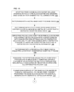
[00040] FIGS. 1A-1B are flow diagrams that illustrate a method for designing a
low
voltage capacitive micromachined ultrasonic transducer (CMUT) according to
some
embodiments herein;
[00041] FIG. 2A is an exemplary diagram that illustrates performing dry
oxidation of a
silicon wafer to obtain a required silicon dioxide (SiO2) thickness of a base
silicon wafer
according to some embodiments herein;
7
CA 03232631 2024- 3- 21
WO 2023/047417
PCT/1N2022/050851
[00042] FIG. 2B is an exemplary diagram that illustrates depositing a copper
(Cu) or
aluminium (Al) metal (MI) layer with a required thickness over the base oxide
(SiO2) according
to some embodiments herein:
[00043] FIG. 2C is an exemplary diagram that illustrates patterning with a
metal mask and
etching the metal (M1) layer to create a CMUT bottom plate and a metal (M1)
interconnect layer
according to some embodiments herein;
[00044] FIG. 2D is an exemplary diagram that illustrates depositing a
dielectric layer using
Plasma-Enhanced Chemical Vapor Deposition (PECVD) over an entire silicon wafer
according
to some embodiments herein:
[00045] FIG. 2E is an exemplary diagram that illustrates patterning with a
Field Oxide
(FOX) Mask and etching the PECVD Oxide using buffer Hydrogen Fluoride (HF)
solution to
obtain CMUT cavities wafer according to some embodiments herein;
[00046] FIG. 2F is an exemplary diagram that illustrates depositing
polysilicon over the
entire silicon wafer according to some embodiments herein;
[00047] FIG. 2G is all exemplary diagram that illustrates subsequently
depositing titanium
(Ti) over doped polysilicon that is deposited on an entire silicon wafer
according to some
embodiments herein;
[00048] FIG. 2H is an exemplary diagram that illustrates subsequently
depositing a
dielectric layer some embodiments herein;
[00049] FIG. 21 is an exemplary diagram that illustrates patterning with a
pedestal¨poly
mask over a dielectric layer that is deposited over the titanium and removing
the patterned
dielectric by a wet etch process according to some embodiments herein;
[00050] FIG. 2J is an exemplary diagram that illustrates removing exposed
titanium by an
alternative wet etch process according to some embodiments herein;
[00051] FIG. 2K is an exemplary diagram that illustrates excavating the
polysil icon inside
the cavity according to some embodiments herein;
[00052] FIG. 2L is an exemplary diagram that illustrates planarising surface
of the base
silicon wafer by chemical mechanical polishing (CMP) according to some
embodiments herein;
[00053] FIG. 2M is an exemplary diagram that illustrates starting with a
separate top
silicon wafer including a silicon "device" layer on top of buried oxide grown
over a thick
"handle" silicon layer according to some embodiments herein;
8
CA 03232631 2024- 3- 21
WO 2023/047417
PCT/1N2022/050851
[00054] FIG. 2N is an exemplary diagram that illustrates depositing a Metal 2
over an
entire wafer surface according to some embodiments herein;
[00055] FIG. 20 is an exemplary diagram that illustrates patterning with a
Metal 2 Mask
and etching the Metal 2 according to some embodiments herein;
[00056] FIG. 2P is an exemplary diagram that illustrates patterning with a
CMUT Cell
mask and etching the silicon "device" layer to define a CMUT top plate
according to some
embodiments herein;
[00057] FIG. 2Q is an exemplary diagram that illustrates aligning the separate
top silicon
wafer and the base silicon wafer according to some embodiments herein;
[00058] FIG. 2R is an exemplary diagram that illustrates chemical mechanical
polishing
(CMP) of the handle silicon layer by the RIE and a buried oxide layer by a wet
etch process
according to some embodiments herein;
[00059] FIG. 2S is an exemplary diagram that illustrates depositing a Polymer
layer over
an entire wafer according to some embodiments herein;
[00060] FIG. 2T is an exemplary diagram that illustrates patterning with a
Polymer Mask
and selectively etching the Polymer according to some embodiments herein;
[00061] FIG. 3 is a cross-sectional view of a Type 1 CMUT Cell according to
some
embodiments herein;
[00062] FIG. 4 is a cross-section view of Type 2 capacitive micromachined
ultrasonic
transducer (CMUT) according to some embodiments herein;
[00063] FIG. 5A is a cross-section view of Type 3 capacitive micromachined
ultrasonic
transducer (CMUT) according to some embodiments herein;
[00064] FIG. 5B is a cross-section view of Type 4 capacitive micromachined
ultrasonic
transducer (CMUT) according to some embodiments herein;
[00065] FIG. 6 is a graphical representation that depicts Collapse Voltage as
a function of
a membrane radius in gm for collapsed mode (CM) for membrane gap from 0.1 gm,
0.15 gm,
0.2 gm, and 0.25 gm according to some embodiments herein;
[00066] FIG. 7 is a graphical representation that depicts a normalised
effective gap of a
membrane for special structures in a cavity according to some embodiments
herein; and
[00067] FIG. 8 is a graphical representation that depicts dependence of
collapse voltage on
size of a structure according to some embodiments herein.
9
CA 03232631 2024- 3- 21
WO 2023/047417
PCT/1N2022/050851
DETAILED DESCRIPTION OF PREFERRED EMBODIMENTS
[00068] The embodiments herein and the various features and advantageous
details thereof
are explained more fully with reference to the non-limiting embodiments that
are illustrated in
the accompanying drawings and detailed in the following description.
Descriptions of well-
known components and processing techniques are omitted so as to not
unnecessarily obscure the
embodiments herein. The examples used herein are intended merely to facilitate
an
understanding of ways in which the embodiments herein may be practiced and to
further enable
those of skill in the art to practice the embodiments herein. Accordingly, the
examples should
not be construed as limiting the scope of the embodiments herein.
[00069] As mentioned, there remains a need for a capacitive micromachined
ultrasonic
transducer (CMUT) with a high electric field and high membrane capacitance
achieved by
introducing special structures in membrane cavity, thereby reducing an
effective gap between a
membrane and a bottom plate of the CMUT and increasing electromechanical
transduction
efficiency, which is a product of electric field and membrane capacitance.
[00070] The CMUT has a "pedestal" inside the cavity to control the onset of
the deep
collapse. Additionally, a conductor deposition step that further simplifies
the modelling of
capacitance in deep collapse leads to a simplified circuit design based on a 3-
port small signal
equivalent circuit model.
[00071] Further, a double metal process uses different layers of metal for the
lower and
upper plates of the CMUT, thereby enabling row-column addressing of the CMUT
array to
simplify the Drive Electronics.
[00072] There are four alternative implementations of the CMUT array. The
first type of
CMUT is significantly simpler, sits entirely above the silicon surface, has a
conducting pedestal
inside the cavity on the bottom wafer with a dielectric on top of the
pedestal, and therefore a
good fit for post-integration to the Drive / Receive Electronics implemented
in hulk CMOS in a
Back-End Of the Line (BEOL) module. This can be accomplished either by using
Through-
Silicon-Via (TSV), which is not a high-yield technology yet, or by a Chip-on-
Board (COB) or
equivalent bonding technique.
[00073] The second type of CMUT also sits entirely above the silicon surface,
has a
conducting pedestal inside the cavity on the bottom wafer with a dielectric on
the bottom of the
device layer in the top wafer and may be a good fit in certain cases of post-
integration to the
CA 03232631 2024- 3- 21
WO 2023/047417
PCT/1N2022/050851
Drive / Receive Electronics implemented in bulk CMOS in a Back-End Of the Line
(BEOL)
module. This can be accomplished either by using Through-Silicon-Via (TSV),
which is not a
high-yield technology yet, or by a Chip-on-Board (COB) or equivalent bonding
technique.
[00074] The fourth type of CMUT uses isolated wells below each CMUT element.
These
Wells can be maintained at different potentials with respect to the substrate.
Using diffusion in
these (isolated) Wells as one plate of a linear capacitor and the Metal 1 as
the other plate with
SiO2 of suitable thickness as a dielectric, a high-valued constant capacitor
can be created. When
this diffusion layer is shorted to the top plate (M2) of the CMUT, a large,
fixed value capacitance
is effectively placed in parallel to the CMUT, thereby providing a mechanism
to independently
increase the CMUT capacitance and reduce the effect of interconnect parasitic
on its
performance.
[00075] It is possible to achieve this in a BEOL module using Metal 1 and the
doped
pedestal Polysilicon as the two plates of this linear capacitor. There may be
other similar ways to
accomplish this as well.
[00076] The use of titanium as gettering material is used to improve the
cavity vacuum
without using high-cost equipment. An ultrasound range transparent polymer is
used which
enhances the membrane peak deflection, which in turn increases the output
ultrasound pressure
for imaging and other applications.
[00077] A metal interleaved insulator structure is used to enhance the
membrane peak
deflection and by reducing the membrane to the pedestal gap it enhances the
electric field and
capacitance. This in turn enhances the electro-mechanical transduction
efficiency.
[00078] All the new structures represented by first, second, third, and fourth
types provide
the capability of operating the CMUT cells at low dc voltages in collapse
mode. This provides
higher beam deflection and in turn higher output ultrasound pressure. These
are the salient
features that improve the performance of the CMUT cell. The CMUT does not
require ultra-high
vacuum packaging requirement. The intended performance of vacuum packaging is
alternatively
accomplished using the gettering material.
[00079] A polymer on top of the membrane facilitates high membrane deflection
and long
life of the CMUT device. The selected polymer is such that it is transparent
to the ultrasound
frequency range of choice for the CMUT in question. In addition, the thickness
of the polymer is
chosen in a way such that it enhances the beam deflection. However, the use of
polymer and its
11
CA 03232631 2024- 3- 21
WO 2023/047417
PCT/1N2022/050851
thickness dependence on the membrane deflection for higher output pressure has
not been
explored.
[00080] The problems of existing PZT-based imaging transducers have been
addressed and
solved with high range resolution and sensitivity CMUT-based array transducers
that are ROHS
compliant. Further, the new CMUT-based device configuration is inducted with a
special
structure to reduce the collapse voltage to operate the devices at low dc
voltages. In addition, the
device can be fabricated using standard process steps of a conventional
semiconductor foundry.
[00081] A 2-level metallization process is unique to the structure shown where
the
electronic circuitry and the membrane cavity can be independently processed
and upgraded as
the State of Art improves. Referring now to the drawings, and more
particularly to Figs. lA
through 8, where similar reference characters denote corresponding features
consistently
throughout the figures, there are shown preferred embodiments.
[00082] FIGS. 1A-1B are flow diagrams that illustrate a method for designing a
low
voltage capacitive micromachined ultrasonic transducer (CMUT) according to
some
embodiments herein. At step 102, started from a base silicon wafer includes
starting with a N-
type Silicon Wafer and growing base oxide by performing the following steps.
At step 104, a
metal mask is patterned over the base oxide. At step 106, a Field Oxide (FOX)
Mask is patterned
over a copper (Cu) or Aluminium (Al) metal (M1) layer that is deposited over
the base oxide. At
step 108, polysilicon is deposited over the entire silicon wafer and the
polysilicon is doped with a
donor species with a concentration approaching its respective solid solubility
limit, titanium (Ti)
is subsequently deposited over the doped polysilicon that is deposited on the
entire silicon wafer
and a dielectric layer subsequently deposited. In some embodiments, the
dielectric layer is
Silicon Dioxide or in a stack with Hafnium Oxide or alternatively in a stack
with Silicon Nitride
or a high relative permittivity material.
[00083] At step 110, a pedestal¨poly is patterned mask over a dielectric layer
that is
deposited over the titanium. At step 112, the patterned dielectric is removed
by a wet etch
process and exposed titanium is subsequently removed by an alternative wet
etch process and
sequentially excavating by reactive ion etch (RIE) all exposed polysilicon. At
step 114, surface
of the base silicon wafer is planarized surface of the base silicon wafer by
chemical mechanical
polishing (CMP), thereby preparing the base silicon wafer for eventual bonding
with a separate
top silicon wafer by chemical mechanical polishing (CMP), thereby preparing
the base silicon
12
CA 03232631 2024- 3- 21
WO 2023/047417
PCT/1N2022/050851
wafer for eventual bonding with a separate top silicon wafer. At step 116,
started with the
separate top silicon wafer including a silicon "device" layer on top of buried
oxide grown over a
thick "handle" silicon layer and perform the following steps. At step 118, an
aluminium layer is
deposited by sputtering. The aluminium layer is Metal 2. At step 120, a Metal
2 Mask is
patterned and the Metal 2 is etched by a wet etch process. At step 122, a CMUT
Cell mask is
patterned and the silicon "device" layer is etched by RIE to define a CMUT top
plate. At step
124, the separate top silicon wafer and the base silicon wafer are aligned to
enable the Metal 2 of
the separate top silicon wafer to align with Pillar Poly of the base silicon
wafer; and the separate
top silicon wafer and the base silicon wafer are heated to enable the Metal 2
of the separate top
silicon wafer to align with Pillar Poly of the base silicon wafer, and to (a)
form a eutectic
bonding between the polysilicon and aluminium during which a certain thickness
of the Metal 2
is consumed, and (b) form a Polycide between the Polysilicon and the Titanium
(Ti) alloy in
parallel. The Titanium present inside the cavity (i) acts as a getter when the
eutectic bonding is
happening between the polysilicon and aluminium, (ii) forms chemical bonds
with residual
Nitrogen and Oxygen, and (c) removes the residual Nitrogen and Oxygen from the
cavity,
thereby improving vacuum in the cavity. At step 126, a Polymer layer is
deposited over an entire
wafer. At step 128, a Polymer Mask is patterned and the Polymer is selectively
etched to (a)
isolate CMUT cells from mechanical coupling and (b) remove the polymer at bond
pads.
[00084] In some embodiments, the N-Type Silicon Wafer is replaced by P-Type
Silicon
Wafer. In some embodiments, concentration of the N-type Silicon Wafer is 5 x
1015/cm3,
wherein the base oxide has 0.5 pm thickness.
[00085] In some embodiments, the method includes performing dry oxidation of a
silicon
wafer to obtain a required silicon dioxide (SiO2) thickness of the base
silicon wafer, the dry
oxidation is performed at 1050 C for an appropriate time interval. The
required oxide thickness
is 1 pm. In some embodiments, the method includes depositing the copper (Cu)
or aluminium
(Al) metal (M1) layer with a required thickness over the base oxide (SiO2), In
some
embodiments, a thickness of the copper or Al metal 1 layer is based on a
design specification of
resistivity.
[00086] In some embodiments, the method includes etching the copper/A1 metal
using a
wet etch process to create a CMUT bottom plate and a metal (M1) interconnect
layer after the
13
CA 03232631 2024- 3- 21
WO 2023/047417
PCT/1N2022/050851
metal mask is patterned over the base oxide; and depositing conformally SiO2
using Plasma-
Enhanced Chemical Vapor Deposition (PECVD) over an entire silicon wafer.
[00087] In some embodiments, the method includes etching the PECVD SiO2 after
the
Field Oxide (FOX) Mask is patterned using buffer Hydrogen Fluoride (HF)
solution to obtain
CMUT cavities.
[00088] In some embodiments, the method includes etching the dielectric layer
using the
wet etch process to expose the titanium from all areas where underlying poly
is to be etched,
wherein the dielectric layer is at least one of SiO2, SiO2 / Hf02 sandwich or
SiO2 / Si3N4
sandwich.
[00089] In some embodiments, the method includes etching the Titanium by the
wet-etch
process where the polysilicon acts as an "etch-stop", wherein the Titanium
(Ti) is deposited over
the polysilicon with a thickness of 100 nm by sputtering.
[00090] In some embodiments, the method includes excavating the polysilicon
inside
cavity around the pedestal and regions adjacent to pillars to prevent shorting
of adjacent CMUTs.
[00091] In some embodiments, the Chemical Mechanical Polishing (CMP) is
performed on
the polysilicon with a thickness of 1.4 pm to remove the excess dielectric on
the pillar; and the
titanium (Ti) on pillar polysilicon and the excess height of the polysilicon
to render the surface of
a wafer planar.
[00092] In some embodiments, the method includes chemical mechanical polishing
(CMP)
of the handle silicon layer by RIE and, sequentially, a buried oxide layer by
the wet etch process.
[00093] In some embodiments, the separate top silicon wafer comprises a
heavily doped
top n+ silicon layer that is intended to be a membrane with a thickness of 2
p.m. In some
embodiments, the separate top silicon wafer comprises the thick handle silicon
layer that is
removed by RIE and the buried oxide layer placed below with the thickness of
0.5 pm which is
removed by the wet-etch process with the silicon device layer acting as etch-
stop for its removal.
[00094] In some embodiments, the Metal 2 of thickness 0.8 pm is reduced to 0.4
pm
during eutectic bonding at 600 C and a 0.1 pm thick membrane dielectric leaves
a gap of 0.3 pm.
In some embodiments, different combinations of the Metal 2 thickness and
membrane dielectric
thickness are used to control gap between the membrane and the pedestal and
different sandwich
stacks to simultaneously achieve a desired capacitance value of the CMUT
independent of the
gap thickness.
14
CA 03232631 2024- 3- 21
WO 2023/047417
PCT/1N2022/050851
[00095] In some embodiments, two plates of the CMUT embodied as the Metal 1
and the
Metal 2 are isolated from corresponding plates of other CMUT cells on a same
die, this isolation
enabling compensation of stray capacitances by suitable circuit techniques.
[00096] In some embodiments, a pedestal in one or more sizes and one or more
shapes
comprising interleaved and grid-like structures is constructed inside the
cavity of the CMUT. In
some embodiments, the pedestals enable lowering of the collapse voltage,
enable lowering of
operating voltages and improve control on a resonant frequency of vibration of
the membrane.
[00097] FIG. 2A is an exemplary diagram 201 that illustrates performing dry
oxidation of
a silicon wafer 202 to obtain a required silicon dioxide (SiO2) thickness of a
base silicon wafer
according to some embodiments herein. The exemplary diagram 201 includes the
silicon wafer
and silicon dioxide (SiO2) 204. In some embodiments, the dry oxidation is
performed at 1050 C
for an appropriate time. In some embodiments, the required oxide thickness is
1 m. The
functions of these components have been explained above.
[00098] FIG. 2B is an exemplary diagram 203 that illustrates depositing a
copper (Cu) or
aluminium (Al) metal (M1) layer 206 with a required thickness over the base
oxide (SiO2) 204
according to some embodiments herein. In some embodiments, the copper or Al
metal 1 layer
206 is deposited with a thickness of 0.2 [rm. The functions of these
components have been
explained above.
[00099] FIG. 2C is an exemplary diagram 205 that illustrates patterning with a
metal mask
over the base oxide 204 according to some embodiments herein. The functions of
these
components have been explained above.
[000100] FIG. 2D is an exemplary diagram 207 that illustrates depositing a
dielectric layer
according to some embodiments herein. In some embodiments, the dielectric
layer is deposited
with a thickness of 1.5 gm using the PECVD. The functions of these components
have been
explained above.
[000101] FIG. 2E is an exemplary diagram 209 that illustrates patterning with
a Field
Oxide (FOX) Mask and etching the PECVD Oxide using buffer Hydrogen Fluoride
(HF)
solution to obtain CMUT cavities wafer according to some embodiments herein.
The functions
of these components have been explained above.
[000102] FIG. 2F is an exemplary diagram 211 that illustrates depositing
polysilicon 208
over the entire silicon wafer according to some embodiments herein. The
polysilicon 208 is
CA 03232631 2024- 3- 21
WO 2023/047417
PCT/1N2022/050851
deposited over the entire silicon wafer and the polysilicon 208 is doped with
a donor species with
a concentration approaching its respective solid solubility limit. In some
embodiments, the
polysilicon 208 is deposited on the etched PEVCD Oxide with the thickness of 2
iLtm using Low-
Pressure Chemical Vapor Deposition (LPCVD).
[000103] FIG. 2G is an exemplary diagram 213 that illustrates subsequently
depositing
titanium (Ti) over the doped polysilicon that is deposited on the entire
silicon wafer according to
some embodiments herein. The functions of these components have been explained
above.
[000104] FIG. 2H is an exemplary diagram 215 that illustrates subsequently
depositing a
dielectric layer 212 some embodiments herein. The dielectric layer 212 is
Silicon Dioxide or in a
stack with Hafnium Oxide or alternatively in a stack with Silicon Nitride or a
high relative
permittivity material.
[000105] FIG. 21 is an exemplary diagram 217 that illustrates patterning with
a pedestal¨
poly mask over the dielectric layer 212 that is deposited over the titanium
210 and removing the
patterned dielectric by a wet etch process according to some embodiments
herein. The functions
of these components have been explained above.
[000106] FIG. 2J is an exemplary diagram 219 that illustrates removing exposed
titanium
by an alternative wet etch process according to some embodiments herein. The
functions of these
components have been explained above.
[000107] FIG. 2K is an exemplary diagram 221 that illustrates excavating the
polysilicon
208 inside the cavity according to some embodiments herein. The polysilicon
208 inside the
cavity is excavated and the pedestal is formed by an anisotropic Reactive Ion
Etch (RIE) with a
photoresist protecting the Ti 210. The pedestal is a structure that controls
onset of deep collapse.
[000108] FIG. 2L is an exemplary diagram 223 that illustrates planarising
surface of the
base silicon wafer by chemical mechanical polishing (CMP) according to some
embodiments
herein. In some embodiments, the Chemical Mechanical Polishing (CMP) is
performed on the
polysilicon 208 with a thickness of 1.4 i.tm to remove the Titanium (Ti) 210
on pillar polysilicon
and the excess height of the polysilicon 208 to render the surface of a wafer
planar.
[000109] FIG. 2M is an exemplary diagram 225 that illustrates starting with a
separate top
silicon wafer including a silicon "device" layer on top of buried oxide 216
grown over a thick
"handle" silicon layer according to some embodiments herein. In some
embodiments, the
separate top silicon wafer includes a heavily doped top n+ silicon layer 218
that is intended to be
16
CA 03232631 2024- 3- 21
WO 2023/047417
PCT/1N2022/050851
a membrane with a thickness of 2 pm. In some embodiments, the separate top
silicon wafer
includes the thick handle silicon layer that is removed by the RIE and the
buried oxide layer 216
placed below with the thickness of 0.5 pm which is removed by the wet-etch
process with the
silicon device layer acting as etch-stop for its removal.
[000110] FIG. 2N is an exemplary diagram 227 that illustrates depositing a
Metal 2 220
over an entire wafer surface according to some embodiments herein. In some
embodiments, the
Metal 2 220 is deposited over the entire top wafer with a thickness of 0.8
tim.
[000111] FIG. 20 is an exemplary diagram 229 that illustrates patterning with
a Metal 2
Mask and etching the Metal 2 220 according to some embodiments herein. The
functions of
these components have been explained above.
[000112] FIG. 2P is an exemplary diagram 231 that illustrates patterning with
a CMUT
Cell mask and etching the silicon "device" layer to define a CMUT top plate
according to some
embodiments herein. The functions of these components have been explained
above.
[000113] FIG. 2Q is an exemplary diagram 233 that illustrates aligning the
separate top
silicon wafer and the base silicon wafer according to some embodiments herein.
The separate top
silicon wafer and the base silicon wafer are aligned to enable the Metal 2 220
of the separate top
silicon wafer to align with Pillar Poly of the base silicon wafer, and the
separate top silicon wafer
and the base silicon wafer are heated to (a) form a eutectic bonding between
the polysilicon and
aluminium during which a certain thickness of the Metal 2 220 is consumed, and
(b) form a
Polycide between the Polysilicon and the Titanium (Ti) alloy in parallel. The
Titanium present
inside the cavity (i) acts as a getter when the eutectic bonding is happening
between the
polysilicon and aluminium, (ii) forms chemical bonds with residual Nitrogen
and Oxygen, and
(c) removes the residual Nitrogen and Oxygen from the cavity, thereby
improving vacuum in the
cavity.
[000114] In some embodiments, the Metal 2 220 of thickness 0.8 pm is reduced
to 0.4p
during eutectic bonding at 600 C and a 0.1 pm membrane dielectric leaves a gap
of 0.3 pm. In
some embodiments, different combinations of the Metal 2 220 thickness and
membrane
dielectric thickness are used to control gap between the membrane and the
pedestal and different
sandwich stacks to simultaneously achieve a desired capacitance value of the
CMUT
independent of the gap thickness.
17
CA 03232631 2024- 3- 21
WO 2023/047417
PCT/1N2022/050851
[000115] FIG. 2R is an exemplary diagram 235 that illustrates chemical
mechanical
polishing (CMP) of the handle silicon layer by the RIE and a buried oxide
layer by a wet etch
process according to some embodiments herein. The functions of these
components have been
explained above.
[000116] FIG. 2S is an exemplary diagram 237 that illustrates depositing a
Polymer layer
222 over an entire wafer according to some embodiments herein. The functions
of these
components have been explained above.
[000117] FIG. 2T is an exemplary diagram 239 that illustrates patterning with
a Polymer
Mask and selectively etching the Polymer 222 according to some embodiments
herein. The
Polymer Mask is patterned, and the Polymer 222 is selectively etched to (a)
isolate CMUT cells
from mechanical coupling and (b) remove the polymer at bond pads.
[000118] FIG. 3 is a cross-sectional view of a Type 1 CMUT Cell 300 according
to some
embodiments herein. The cross-sectional view of the Type 1 CMUT Cell 300
includes the silicon
wafer 202, the silicon dioxide (SiO2) 204, the metal 1 (M1) 206, the
polysilicon 208, the
Titanium 210, the heavily doped top n+ silicon layer 218, the Metal 2 220, and
the polymer 222.
In some embodiments, the CMUT 300 doesn't include bulk silicon and can be
constructed
entirely using two metals such as the metal 1 (M1) 206 and the metal 2 (M2)
220. In some
embodiments, membrane dielectric can be for example a 100 nm layer of silicon
dioxide grown
by dry oxidation. In some embodiments, a resonant frequency of the CMUT 300 is
determined
using geometry and material properties of the CMUT 300.
[000119] In some embodiments, a multi-frequency CMUT is obtained by exploiting
two
properties of CMUTs by (i) making a cluster of a finite number of
interconnected CMUTs where
each has a different resonant frequency and (ii) exploiting a property, where
possible, that a
given CMUT apart from its fundamental resonance also exhibits overtone type
higher order
resonance modes_ In some embodiments, the cluster of the finite number of
CMUTs is referred
as a CMUT Element to distinguish it from the CMUT 300. The property may be
exploited to
minimize the number of CMUTs in the cluster while maximizing a number of
discrete
frequencies within a certain pre-determined band.
[000120] In some embodiments the CMUT 300 has 30-120 pm diameter and a centre-
to-
centre spacing to maintain conductors within each unit cell isolated from
adjacent cells, thereby
preventing any dielectric breakdown under normal usage. When configured as an
element that
18
CA 03232631 2024- 3- 21
WO 2023/047417
PCT/1N2022/050851
includes one or more CMUTs depending on a desired frequency range, resolution,
and
sensitivity. In some embodiments, a 15 MHz range for example can be
accomplished with 4 such
cells. In some embodiments, inter-elemental separation is suitably determined
from electrical and
dielectric field breakdown considerations. In some embodiments, an inter-
elemental separation
of the CMUT 300 is 25 inn. Each element of the CMUT 300 is configured as an
array that can be
independently driven while implementing a phase array concept or compressive
sampling. In
some embodiments, a two-dimensional array is designed using the CMUT 300 shown
in FIG. 3
can perform a function of any suitable orthogonal code implementation. The
CMUT 300 can be
designed for higher order multi-frequency oscillations to optimize a number of
cells in the
element, thereby enabling a maximum number of discrete frequencies which may
lower a
number of distinct CMUT cells/elements to cover an entire ultrasonic frequency
band. Further,
multi-frequency oscillations are exploited for automotive applications by
using the spread
spectrum communication which increases a range resolution at lower power
transmission. In
some embodiments, any further multiplexed frequency and higher modal frequency
with
appropriate filleting operation can be used to detect low-flying objects such
as Drones. In some
embodiments, an application of spread spectrum in conjunction with multi-
frequency operation
and reduced sampling technique (compressive sampling) is used for generating
higher modal
frequencies and can be implemented using the CMUT 300.
[000121] In some embodiments, performance evaluation parameters in comparison
with
standard CMUT cells highlighted in the block diagram FIG. 3 can be summarized
to provide
improved performance on i) feasibility of using a smaller radius of the CMUT
300 providing the
capability of operating at a higher frequency (18.836 MHz) with the capability
of using
orthogonal codes for Tx/Rx, ii) higher vacuum in comparison with standard
packaging schemes
by using a gettering layer for residual gas absorption, iii) higher membrane
deflection by the use
of appropriately chosen polymer, which is transparent to an ultrasound
frequency band, iv)
considerably reduced collapse voltage using special structures in the cavity,
which are
conductive and enhances the electrical field, v) enhanced electro-mechanical
transduction
leading to higher output ultrasonic pressure increasing the range resolution,
and vi) use of three
port small signal equivalent circuit model to predict consistency in the
prototype and simulated
devices because of negligible spring softening effect.
19
CA 03232631 2024- 3- 21
WO 2023/047417
PCT/1N2022/050851
[000122] In some embodiments, a starting N-type wafer is at least one of
undoped silicon
or even oxide in a BEOL configuration. In some embodiments, the starting
material is a plane
substrate such as glass. In some embodiments, the photoresist is positive. In
some embodiments,
the positive photoresist is a photoactive polymer that when exposed to UV gets
its bonds broken
so that a subsequent "development" of photoresist results in the field regions
exposed to UV
being dissolved by a chemical process that leaves unexposed regions
undisturbed.
[000123] FIG. 4 is a cross-section view 400 of Type 2 capacitive micromachined
ultrasonic transducer (CMUT) according to some embodiments herein. The cross-
sectional view
of the Type 2 CMUT Cell 400 includes a silicon wafer 402, silicon dioxide
(SiO2) 404, a metal 1
(M1) 406, polysilicon 408, Titanium 410, a heavily doped top n+ silicon layer
412, a Metal 2
414, polymer 416 and membrane dielectric 418. The cross-section view 400
depicts the
sandwiched membrane dielectric 418 in the top wafer to create a high fixed
value capacitance in
Collapse of the CMUT. In some embodiments, the Type 2 can be constructed using
top two
levels of Metal. In some embodiments, the membrane cavity, as in the Type 1
CMUT, has the
pedestal structure to precisely control the effective gap for reducing the
collapse voltage. In some
embodiments, the Type 2 CMUT can be constructed with SiO2 on a membrane
replaced by a
SiO2-Hf02-Si02 sandwich. In some embodiments, the Type 2 CMUT can be
constructed with
SiO2 on a membrane replaced by a SiO2-Si3N4 sandwich. In some embodiments, the
Type 2
CMUT can be constructed with SiO2 on a membrane replaced by a SiO2-Si3N4-SiO2
sandwich.
[000124] FIG. 5A is a cross-section view 500 of Type 3 capacitive
micromachined
ultrasonic transducer (CMUT) according to some embodiments herein. The CMUT
includes a n-
type wafer substrate 502, a n+ type diffusion in a substrate 504, metal 1 (M1)
506, Field Oxide
(FOX: SiO2) 508, an inter-metal dielectric (IMD) 510, metal 2 (M2) 512, a base
oxide layer 514,
n+ doped poly 516, a gettering layer 518, Si membrane n 520 and polymer 522.
In some
embodiments, the n-type wafer 502 is <100> Crystal Orientation Silicon Wafer.
In some
embodiments, concentration of the silicon wafer is 1015/cm3. The CMUT is
fabricated using a
base wafer process and a top SOT Wafer process. The base wafer process of the
CMUT includes
developing base oxide (SiO2) and Nitride (Si3N4) sandwich over the n-type
wafer 502 and
coating photoresist over the base oxide (SiO2) and Nitride (Si3N4) sandwich.
The base wafer
process includes making an N+ Mask (Light Field) by developing the
photoresist, etching the
CA 03232631 2024- 3- 21
WO 2023/047417
PCT/1N2022/050851
base oxide (SiO2) and the Silicon Nitride (Si3N4) from field regions, and
thermally growing or
depositing Field Oxide (FOX: SiO2).
[000125] The base wafer process further includes stripping the photoresist and
etching the
base oxide (SiO2) and the Silicon Nitride (Si3N4). The base wafer process
further includes
implanting high concentration and low energy n+ type dopants such as the n+
type substrate
diffusion 504, depositing the M1 506, and driving the M1 506 in the n+ type
substrate 504. In
some embodiments, the M1 506 is used to stop out-gassing during drive-in.
[000126] The base wafer process further includes growing thin oxide thermally
over the
MI 506, depositing polysilicon on the thin oxide, and doping the poly with n+
to solid solubility
limit. The base wafer process further includes depositing Si3N4 over the doped
poly with n+ 516
and coating the photoresist over the Si3N4.
[000127] In some embodiments, Poly height is calculated by
Poly height = flat portion of a top plate of the CMUT + pedestal height
[000128] In some embodiments, Nitride height is calculated by
Nitride height = CMUT cavity height ¨ Poly height.
[000129] The base wafer process further includes making a Metal 1 Mask (LF) by
developing the photoresist over the Metal 1 Mask (LF), etching Nitride, and
etching Poly from
non- CMUT regions. The base wafer process further includes etching the M1 506
and stripping
the photoresist and coating the photoresist.
[000130] The base wafer process further includes making a CMUT Membrane Mask
by
developing the photoresist over the CMUT Membrane Mask and etching the Nitride
and the
Poly. The base wafer process further includes growing the Inter-Metal
Dielectric (IMD) 510,
stripping the photoresist, and coating fresh photoresist.
[000131] The base wafer process further includes making a CMUT Pedestal Mask
(Dark
Field (DF) by developing the photoresist over the CMUT Pedestal Mask (DF) and
etching the
Nitride and the Poly. The base wafer process further includes depositing the
poly (base
conducting layer of the top plate), doping the n 504 on the Poly to solid
solubility limit,
stripping the photoresist, and subsequently coating the photoresist. The n+
dopant is implanted
with a high concentration and low energy. In some embodiments, Deep Reactive
Ion Etching
(DRIE) is employed to etch out an annular cavity around the CMUT Pedestal Mask
(DF). The
CMUT Pedestal Mask (Dark Field (DF)) is made by developing the photoresist
over the CMUT
21
CA 03232631 2024- 3- 21
WO 2023/047417
PCT/1N2022/050851
Pedestal Mask (DF) and etching the Nitride and the Poly. The CMUT Pedestal
Mask (Dark Field
(DF) is made by depositing the poly (base conducting layer of the top plate),
doping the n+ 504
on the Poly to solid solubility limit, stripping the photoresist, and coating
the photoresist.
[000132] The base wafer process further includes making a CMUT Poly Mask (LF)
by
developing the photoresist over the CMUT Poly Mask (LF), etching the Poly over
the IMD 510,
stripping the photoresist, and etching the Nitride.
[000133] The top SOT Wafer process includes starting with a top SOT Silicon
wafer with
an 1\1- type <100> device layer with a buried SiO2 layer with a top silicon
handle layer. In some
embodiments, concentration of the N- device layer is 1018/cm3. The top SOT
Wafer process
includes etching device silicon to desired (membrane) thickness, depositing
titanium (getter) on
the silicon device layer, bonding it to the base wafer, removing the handle,
and coating the
photoresist.
[000134] The top SOT Wafer process includes making the CMUT Membrane Mask (LF)
with slight oversizing by developing the photoresist, etching SiO2, and
etching Si from non-
CMUT areas. The top SOT Wafer process further includes stripping and coating
fresh
photoresist. The top SOT Wafer process further includes making via Mask (DF)
by developing
the photoresist, etching the IMD 510 via contacts and SiO2 over the membrane,
stripping the
photoresist, depositing the Metal 2 512, and coating fresh photoresist over
the Metal 2 512.
[000135] The top SOT Wafer process further includes making the Metal 2 512
(LF) by
developing the photoresist, etching the Metal 2 512, stripping the
photoresist, depositing the
Polymer 522, and coating the photoresist. The top SOT Wafer process further
includes making
the Polymer mask (LF) by developing the photoresist, etching the Polymer 522,
and stripping the
photoresist. In some embodiments, the Polymer mask (LF) is oversize than the
CMUT
Membrane Mask.
[000136] FIG. 5B is a cross-section view 501 of Type 4 capacitive
micrornachined
ultrasonic transducer (CMUT) according to some embodiments herein. The CMUT
includes a n-
type wafer substrate 502, a n type diffusion in a substrate 504, metal 1 (M1)
506, Field Oxide
(FOX: SiO2) 508, an inter-metal dielectric (IMD) 510, metal 2 (M2) 512, a base
oxide layer 514,
n+ doped poly 516, a gettering layer 518, Si membrane n 520 and polymer 522.
In this
implementation, the type 5 of CMUT can be constructed with a Linear Capacitor
sandwiched
below the CMUT as shown in FIG. 5B either using Diffusion or Poly or Metal for
each plate of
22
CA 03232631 2024- 3- 21
WO 2023/047417
PCT/1N2022/050851
this linear capacitor. In some embodiments, a combination of n+ well in p-well
realized on an n-
type substrate. In some embodiments, the Type 4 of the CMUT includes the
sandwiched nitride
and oxide layer to create a high fixed value capacitance that sits in parallel
to the CMUT. In an
integrated implementation this Type 4 can be constructed using the top two
levels of Metal
combined with a linear capacitor module if available. The membrane cavity, as
in the Type 3
CMUT, has a special structure to decrease the effective gap for reducing the
collapse voltage.
[000137] In some embodiments, a resonant frequency is primarily determined by
the
Young's Modulus, the Poisson's ratio, elastic constant, which are the primary
physical
parameters of the membrane in conjunction with membrane thickness and its
radius.
[000138] In some embodiments of Type 1 and Type 2 CMUTs the resonant frequency
of
the CMUT typically reduces by a factor of 9% with increasing membrane radius
for a fixed
membrane thickness of 1.5 j.im. The percentage decrease in frequency is about
11% as the
membrane thickness reduces to about 1 !am. The fundamental mode of vibration
will depend on
the external force exerted on the membrane and the radius of the membrane in
conjunction with
the membrane thickness.
[000139] Table 1 shows the frequency dependence as a function of the membrane
radius
for a few values of membrane thicknesses from 1 p.m to 1.5 1..tm and a fixed
gap "tg" of 0.25 ji in
a Type 1 Si/SiO2 membrane structure,
Radius vim Frequency in MHz Frequency in MHz for Frequency in
fort 1.1.m thick 1.25 mm thick MHz for 1.5
pm
membrane membrane thick membrane
18 11.2 14.1 16.9
9.1 11.4 13.7
22 7.5 9.4 11.3
24 6.35 7.9 9.52
26 5.4 6.7 8.1
28 4.6 5.8 7
4.06 5.07 6.1
32 3.56 4.46 5.35
34 3.16 3.95 4.74
36 2.82 3.52 4.23
38 2.5 3.16 3.79
2.28 2.85 3.4
1.8 2.25 2_7
1.4 1.82 2.18
1.2 1.51 1.81
23
CA 03232631 2024- 3- 21
WO 2023/047417
PCT/1N2022/050851
[000140] Since, the collapse voltage also depends on the membrane thickness,
and its gap,
therefore a judicious tradeoff is required to be made between these parameters
to achieve a low
collapse voltage. The radius of the CMUT is used to determine the operating
frequency as a
function of membrane gap. There are options of reducing the collapse voltage:
a) reducing the
membrane gap for a given thickness and membrane radius, b) by reducing the
membrane
effective gap (vacuum gap + dielectric thickness / dielectric constant of
insulating layer), c)
using the dielectric special structure (pedestal) in the cavity, and d) making
the judicious choice
of the special structure in the cavity of conducting layer with very low
resistivity.
[000141] Table 2 Collapse mode of operation of Si-SiO2 structure using
dielectric
pedestal in the membrane cavity.
Radius Membrane Membrane gap "tg" "Membrane gap Membrane gap "tg"
I-1 gap "tg" 0. 2u. "tg" 0.15u. 0.125u
0.25[1
18 103 73.76 47.99
36.46
22 69 49.38 32.12
24.42
26 49.4 35.35 23
17.47
30 37.1 26.55 17.27
13.127
34 28.89 20.67 13.45
10.22
38 23.13 16.55 10.76
8.18
42 18.93 13.548 8.81
6.69
46 15.78 11.29 7.34
5.583
50 13.36 9.56 6.22
4.72
[000142] A lowered collapse voltage of the membrane is achieved by increasing
the
electric field in the cavity for the same physical parameters of the CMUT
cell. However, the
radius of the membrane, the membrane thickness and the membrane gap affect the
collapse
voltage. Larger the membrane radius, and/or smaller the membrane thickness
and/or smaller is
the membrane gap, it be will easier to collapse the membrane at lower DC
voltages.
[000143] For smaller radius where the arch of the membrane deflection is
small, the
CMUT cell operates at higher frequencies but the membrane deflection is not
adequate to
collapse the membrane. Therefore, it is desirable to induct special
dielectric/conducting structure
in the membrane cavity to enhance the electric field by reducing the effective
membrane gap of
the cavity.
24
CA 03232631 2024- 3- 21
WO 2023/047417
PCT/1N2022/050851
[000144] The effect of using a dielectric stack in the membrane cavity is
shown in Fig. 3
for standard Si-SiO2 structure, where the SiO2 layer can be changed by a
dielectric stack. These
results are for example shown for a constant membrane thickness of 1.25 pin
for all values of
radii and membrane gap as shown in Table 2. In the solution disclosed here, as
an example a
pedestal with a diameter of 0.75 times of the membrane diameter is inducted in
the cavity for all
physical membrane gaps. The effect of introducing the pedestal in the membrane
cavity is
evident for smaller radius (18 m) with relatively large membrane gap (0.25
m) in column 1
and 2 of Table 2, because it enhances the electric field thereby decreases the
collapse voltage.
The results show the collapse voltage getting reduced by 50% for Si-SiO2 for
smaller radius and
about 40% for larger radius.
[000145] FIG. 6 is a graphical representation 600 that depicts shows Collapse
Voltage as a
function of a membrane radius in pm for collapsed mode (CM) for membrane gaps
0.1 pm, 0.15
pm, 0.2 pm, and 0.25 pm for a collapse mode (CM) according to some embodiments
herein. In
FIG. 6 of the graphical representation 600, the membrane radius in p.m is
plotted on an X-axis
and the collapse voltage in volts is plotted on a Y-axis.
[000146] The graphical representation 600 depicts dependence of the collapse
voltage on
the membrane gap as a function of the membrane radius as the membrane radius
is varied from
18 pm to 50 pm for membrane gaps of 0.125 pm, 0.15 m, 0.20 m, and 0.25 m.
In some
embodiments, the CMUT 300 operating with the radii in the range of 34 gm to 50
pm can have
its operating voltages reduced to below 40 volts. In some embodiments, the
CMUT 300 can
reduce the Collapse Voltage and thereby lower the operating voltage for a
lower membrane
radius.
[000147] The CMUT cell can be operated at low DC voltage by using a thin
membrane,
and / or smaller membrane gap, together with special structures such as the
pedestal in the
membrane cavity_ A method to control the membrane gap is to reduce the
effective gap which is
defined to be the vacuum gap added to dielectric thickness divided by its
dielectric constant. This
is facilitated by the use of high dielectric constant materials. The use of a
high dielectric layer is
desirable in all the CMUT structures because we need to protect the membrane
from damage
during the collapse mode of operation It is always advantageous to use a high
"k" dielectric
stack such as SiO2 / Hf02, because it reduces the collapse voltage by a factor
of square root of
the dielectric constant. A proper design of thickness of each layer on the
basis of breakdown
CA 03232631 2024- 3- 21
WO 2023/047417
PCT/1N2022/050851
leakage current and finally operating the CMUT cell with a considerably higher
effective
dielectric constant. Additionally, the use of materials with high effective
dielectric constant
increases the membrane capacitance.
[000148] Table 3 Variation of normalized effective gap (gap normalized with
dielectric
constant) of membrane for different values of atmospheric pressure The
membrane thickness,
physical cavity gap, oxide thicknesses for the Si-SiO2 structures are chosen
to be 1.25 m, 0.25
m, and 0.125 tim, respectively.
Normalized Normalized Normalized Normalized Normalized Normalized
Atmospheric gap for radius gap for radius gap for radius gap for radius gap
for radius
pressure 22 26 30 34 38
0.1 0.728 0.772 0.825 0.888
0.957
0.2 0.68 0.722 0.772 0.834
0.909
0.3 0.636 0.675 0.721 0.778
0.85
0.4 0.595 0.63 0.673 0.721
0.786
0.5 0.557 0.589 0.624 0.665
0.72
0.6 0.522 0.55 0.579 0.612
0.655
(17 (1491 0.515 0.5380_563
0.594
0.8 0.462 0.482 0.499 0.517
0.537
(19 0.436 0.452 (1464 (1475
0.485
1 0.411 0.424 0.431 0.436
0.439
[000149] The effective gap is sum of the vacuum gap + dielectric thickness /
its dielectric
constant. Whereas, the physical gap is the sum of the vacuum and dielectric
thickness of the
membrane cavity. In present case the physical gap is 0.25 vim, which comprised
of SiO2
thickness to 0.1 ium and 0.15 m of vacuum, then the effective gap is (0.15+
0.1/3.9 = 0.1756
m). The physical gap of the membrane cavity is 0.25 vim and effective gap with
the pedestal is
0.1756 in. The dependence of the effective gap on the pressure is governed by
the change in
capacitance of the membrane for different level of applied pressure. The
capacitance of the
deflected membrane is determined by its radial variation of the deflected
membrane, which is
termed as shape factor. For a given pressure, the shape factor w(r), is
related with the peak
membrane deflection wpk, the radial distance "r" from the fixed end, and the
membrane radius
"a". The shape factor of the membrane deflection is expressed as:
w (r) = wpk (1 - (r2/a2))
26
CA 03232631 2024- 3- 21
WO 2023/047417
PCT/1N2022/050851
[000150] The shape factor for a given applied pressure gets reflected on the
capacitance of
the membrane by the expression given below:
C = CO arctanh Aln. or C/ Co = arctanh \tri
[000151] where Co is the capacitance of the undeflected membrane and 11 = Wpk
tgeffective
[000152] where tgeffõtiõ = vacuum gap + dielectric thickness / its dielectric
constant.
[000153] FIG. 7 is a graphical representation 700 that depicts a normalised
effective gap of
a membrane for special structures in a cavity according to some embodiments
herein. In FIG. 4
of the graphical representation 700, atmospheric pressure is plotted on an X-
axis and pedestal
effective gap normalised to physical gap is plotted on a Y-axis.
[000154] In some embodiments, the membrane radius varies from 22 pm to 38 vm
in steps
of 4 tim. In some embodiments, the membrane thickness of 1.25 pm is selected
for operating the
CMUT 300 at a higher fundamental resonant frequency. In some embodiments, a
physical gap of
the membrane including SiO2 thickness is 0.25 tim, which corresponds to 0.1 pm
of an oxide
layer and 0.15 m of vacuum. The effective gap of the membrane cavity due to
the presence of
the special structure is 0.1777 pm. The incorporation of the special structure
in the membrane
cavity predicting the collapse voltage as a function of atmospheric pressure
is shown in FIG. 7.
[000155] The Collapse Voltage for 38-micron and 20-micron radii for different
fraction
radius sizes is shown in below table 3.
[000156] In some embodiments, results predict a reduction of the effective
membrane gap
by 40% to 60% for atmospheric pressures in the range of 0.4 atmospheric
pressure to 1
atmospheric even at low pressure ranges on the membrane there is a decrease in
the effective gap
of the membrane by 20%. This is a significant result because the collapse
voltage is a square root
of the effective membrane gap thereby very low collapse mode operation of CMUT
devices is
feasible.
[000157] The expression for collapse voltage is 111,21:
8 k
Vcollapse = = ______ (geff Xdc)
i27 co Er A
[000158] Where k is a spring constant, geff is the effective gap, so is a
dielectric constant of
free space, Er iS the relative permittivity of the dielectric material inside
the cavity, A is the area
of the membrane, and (geff-xdo is the peak deflection of the membrane. In some
embodiments,
27
CA 03232631 2024- 3- 21
WO 2023/047417 PCT/1N2022/050851
the equation illustrates that the collapse voltage is very sensitive to the
effective gap of the
membrane. This gap gets considerably reduced by using the special structure in
the membrane
cavity. Therefore, the collapse voltage will be reduced by using the special
structures as
described in Fig. 3.
[000159] The height of pedestal in the membrane cavity gets virtually fixed by
the vacuum
gap of the cavity and the final membrane gap being aimed for the CMUT cell.
However, the
diameter of the pedestal also plays an important role because it facilitates
generation of
multimode vibrations. The effect of radius of the pedestal on the collapse
voltage and it its
dependence on the external pressure has been examined for the pedestal with
0.5 times of the cell
radius for 38 pm, which demonstrate its effect on higher radii devices more
than 50% reduction
in the collapse voltage. For comparison purpose, the effect of pedestal size
of 0.75 and 0.5 times
of the membrane radius of 20 1..tm is evaluated on the collapse voltage. The
effect of using the
pedestal in the membrane cavity has more dominant effect on the collapse
voltage.
Table 4: Dependence of Collapse Voltage on the pressure for fraction of 38 pm
and 20 pm radii
of pedestal size.
Normalized Collapse Collapse Collapse voltage
Atmospheric Voltage for 0. Voltage for for 0.5 times of
pressure 5 times of 38 0.75-times of 20 pm radius
pm radius 20 mn radius
0.1 12.33 40.758 70.14
0.2 11.038 34.65 66.25
0.3 10.06 29.34 60.52
0.4 9.105 24.8 53.85
0.5 8.25 20.95 47.02
0.6 7.502 17.752 40.4
0.7 6.825 15.08 34.4
0.8 6.2328 12.875 29.2
0_9 5_71 11_01 24_719
1 5.24 9.49 20.9
[000160] FIG. 8 is a graphical representation 800 that depicts the dependence
of collapse
voltage on the size of a structure according to some embodiments herein. In
Fig. 8 of the
graphical representation 800, atmospheric pressure is plotted on an X-Axis and
collapse voltage
is plotted on a Y-Axis. The graphical representation 800 depicts a plot of
collapse voltage as a
function of the atmospheric pressure in the range of 0.1 pm to 1.0 pm in the
steps of 0.1 gm. The
28
CA 03232631 2024- 3- 21
WO 2023/047417
PCT/1N2022/050851
fundamental mode of resonant frequency is inversely proportional to the square
of the membrane
radius. In some embodiments, to cover the entire band of desired frequencies,
the membrane
radius is lowered to 22 p.m which results in a fundamental resonant frequency
of 11.4 MHz. In
some embodiments, to cover the lower frequency range, a membrane radius of 38
ium is selected
for which the membrane resonates at 3.16 MHz. This frequency band is good
enough to cover
the entire ultrasound imaging range of 1 MHz to 15 MHz after Golay code /
Phase Coding
implementation.
[000161] The gap of the membrane includes a base oxide layer and vacuum gap
between
the membrane and the oxide layer can be designed to operate the CMUT 300 at a
lowered
collapse voltage based on a selection of base oxide thickness. The results in
Fig. 3 predict that
the CMUT devices with moderate radius (28 i..tm to 38 lam) with the special
structure in the
cavity can be operated below 40 Volts from 0.2 atmospheric pressure to 0.6
atmospheric. The
gap of the cavity, the oxide thickness, and the vacuum between the oxide layer
and the
membrane can be further optimised in accordance with the shape and size of the
special
structures in the membrane cavity. The results are compared for the undamped
natural frequency
which is expressed as:
Undamped frequency wo = Tc-
7 n
[000162] Where k is a spring constant of the membrane material and m is the
effective
mass. Considering the case of <100> silicon this expression for the
fundamental undamped
modal frequency fo gets reduced
1'0 = 0.3656124 x 10⁴ ¨1.2
Where t is the membrane thickness and r is the membrane radius.
[000163] The results of Fig. 8 for the CMUT 300 are described in Fig. 3, with
special
structures in the membrane cavity, reduces the DC voltage below 50 Volts for
atmospheric
pressure ranging from 0.2 to 0.6 because deep collapse mode occurs at lower dc
voltages. The
CMUT small-signal models can predict more accurately the performance of the
CMUT imaging
arrays, because operating the CMUT devices at lower dc voltage the spring
softening effect can
be ignored.
[000164] The analysis carried using out COMSOL Simulink 5.5 with MATLAB for
different membrane radii and highly doped polysilicon layer is shown in Table
5. The analysis of
29
CA 03232631 2024- 3- 21
WO 2023/047417
PCT/1N2022/050851
collapse voltage for different cell radii is also carried out for the
structure shown in Fig 1(a)
using COMSOL Multiphysics 5.5 with MATLAB. The results reported are for
Impulse response
at the operating DC voltage of 40 Volts. The AC response /impulse response has
the cumulative
effect of DC voltage and AC voltage (which is kept as 1 Volt). The DC voltage,
is virtually kept
constant at 40 Volts and cell radius, which is primarily the silicon membrane
excluding the
pillars supporting the membrane and the gap between the polysilicon pedestal
and the pillars
supporting the silicon membrane are as in Fig 1(a). The cell radius is varied
from 52 gm to 92
gm and pedestal radius which is formed primarily by the highly doped
polysilicon is varied from
40 pm to 80 pm.
[000165] Table 5: Dependence of collapse voltage on the cell diameter for a
highly doped
polysilicon pedestal diameter.
DC Voltage (v) and Pedestal Oxide Polysilicon Cell
Collapse Silicon Pedestal 1st Modal Dominant Modal Higer modal
Atmospheric Radius thickness thickness radius Voltage
Thicknesss membrane Frequency Frequency MHz Frequency
Pressure (Pascal) Pm Pm Pm Pm gm gap pro
MHz MHz
40/1E5 40 0.1 1.6 52 24.5 V 2 0.3 14.96
18.836 31.6
40/1E5 40 0.1 1.6 52 24.5 V 2 0.3
18.836 21.135 28.184
40/1E5 40 0.1 1.6 52 25 V 2 0.3 18.836
28.184 31.623
0/1E5 40 0.1 1.6 52 no collpase 2 0.3
14.125 18.836 21.135
40/1E5 40 0.1 1.7 52 25 V 2 0.3 14.125
18.836 31.62
40/1E5 40 0.1 1.7 52 24V 1.5 0.2 14.125
18.836 21.35
40/1E5 52 0.1 1.6 62 24.5V 2 0.3 14.125
18.836 21.35
40/1E5 GO 0.1 1.6 72 25 V 2 3 13.33
18.836 22.387
40/1E5 70 0.1 1.0 80 15 V 2 3 14.125
18.830 19.953
40/1E5 80 0.1 1.6 92 12.5 to 15 V 2 3
14.125 18.836 23.71
[000166] The collapse voltage for smaller cell radius of 52 gm to 80 gm is
typically 24.5
Volts. Whereas, for larger radius above 80 gm the effect of atmospheric
pressure further reduces
the collapse voltage to 15 Volts. An additional feature observed in the
impulse response of the
frequency spectrum had been the dominance of response at 18.836 MHz (typically
intensity of
the peak above 2.78 x 10^7 Pascal) and a sub peak at 14.15 MHz (0.75 x 10^5),
a magnitude
lower than the dominant peak in the desired ultrasonic bandwidth. A higher
mode ranging in the
frequency band of 21 to 31 MHz has also been observed_ However, a dominant
frequency mode
of 2.985 MHz (0.485 x 10^5) and at frequency of 14.125 MHz it is 0.2575 x 10A4
Pascal. For the
collapse voltage of 40 Volts for the polysilicon radius of 38 gm the dominant
peak is at 2.371
MHz with an intensity of 1.04 x 101\5 Pascal.
[000167] The important parameters on the design of a CMUT cell are the range
resolution,
sensitivity and its ease of implementation of spread spectrum in the
transmission and receiver
mode of operation of the CMUT cell. Higher is the resonant / modal frequency
of operation of
CA 03232631 2024- 3- 21
WO 2023/047417
PCT/1N2022/050851
the CMUT cell better is the range resolution. The dominant frequency for the
structures in Fig. 1,
2 is 18.836 MHz which provides the range resolution 81.75 i..tm and
facilitates radiation of more
power by putting up to 5 wavelengths in each bit while implementing the
Golay/phase coding
scheme. The range resolution can be further enhanced by spreading the spectrum
in the
transmission mode and compressing it in the receiver mode of operation.
[000168] The foregoing description of the specific embodiments will so fully
reveal the
general nature of the embodiments herein that others can, by applying current
knowledge, readily
modify and/or adapt for various applications such specific embodiments without
departing from
the generic concept, and, therefore, such adaptations and modifications should
and are intended
to be comprehended within the meaning and range of equivalents of the
disclosed embodiments.
It is to be understood that the phraseology or terminology employed herein is
for the purpose of
description and not of limitation. Therefore, while the embodiments herein
have been described
in terms of preferred embodiments, those skilled in the art will recognize
that the embodiments
herein can be practiced with modification within the spirit and scope of the
appended claims.
20
31
CA 03232631 2024- 3- 21