Note: Descriptions are shown in the official language in which they were submitted.
WO 2023/049328
PCT/US2022/044512
ELECTROCHEMICAL APTAMER SENSORS WITH STABLE
BLOCKING LAYERS, RAPID ELECTRON TRANSFER AND
ROBUST ANTIFOULING PROPERTIES
CROSS-REFERENCE TO RELATED APPLICATIONS
[0001] This application claims priority to, and the benefit of the filing date
of, U.S. Application
Serial No. 63/307,215, titled "Electrochemical Aptamer Sensors with Stable
Blocking Layers,
Rapid Electron Transfer and Robust Antifouling Properties" which was filed on
February 7, 2022
on - the disclosure of which is incorporated by reference herein in its
entirety; and claims priority
to, and the benefit of the filing date of, U.S. Application Serial No.
63/339,196, titled
"Electrochemical Aptamer Sensors with Stable Blocking Layers, Rapid Electron
Transfer and
Robust Antifouling Properties- which was filed on May 6, 2022 - the disclosure
of which is
incorporated by reference herein in its entirety, and the benefit of the
filing date of, U.S. Serial No.
63/248,016, titled "Electrochemical Aptamer Sensor Monolayer Incubation with
Improved
Stability," which was filed September 24, 2021, the disclosure of which is
hereby incorporated
herein by reference in its entirety, and the benefit of the filing date of,
U.S. Application Serial No.
63/282,440, titled "Electrochemical Aptamer Sensors with Non-monolayer
Blocking Layers,"
which was filed on November 23, 2021 - the disclosure of which is incorporated
by reference
herein in its entirety.
FIELD OF THE INVENTION
[0002] This invention relates generally to aptamer sensors, and more
specifically to aptamer
sensors with improved longevity of operation.
BACKGROUND OF THE INVENTION
[0003] This section is intended to introduce the reader to various aspects of
art that may be related
to various aspects of the present invention, which are described and/or
claimed below. This
discussion is believed to be helpful in providing the reader with background
information to
facilitate a better understanding of various aspects of the present invention.
Accordingly, it should
be understood that these statements are to be read in this light, and not as
admissions of prior art.
[0004] Electrochemical aptamer sensors can identify the presence and/or
concentration of an
analyte of interest via the use of an aptamer sequence that specifically binds
to the analyte of
interest. These sensors include aptamers attached to an electrode, wherein
each of the aptamers
has a redox active molecule (redox tag) attached thereto. The redox couple can
transfer electrical
charge to or from the electrode. When an analyte binds to the aptamer, the
aptamer changes shape,
bringing the redox couple closer to or further from, on average, the
electrode. This results in a
measurable change in electrical current that can be translated to a measure of
presence or
- 1 -
CA 03232881 2024- 3- 22
WO 2023/049328
PCT/US2022/044512
concentration of the analyte. When used in this manner, then, aptamers are an
example of an
affinity-based biosensor.
[0005] A major unresolved challenge for aptamer sensors and other affinity-
based biosensors
(particularly those where the aptamers are bonded to the working electrode) is
the lifetime of the
sensors, especially for applications where continuous operation is required
("continuous" referring
to multiple measurements over time by the same device). Such aptamer sensors
are susceptible to
degradation due to, among other things, desorption of the aptamers themselves
from the electrode,
and/or desorption of the blocking layer molecules (such as mercaptohexanol)
from the electrode.
The aptamers and the blocking molecules together form a monolayer which can be
referred to as
a sensing monolayer. The blocking layer portion of the sensing monolayer (1)
ensures that the
aptamer conformation change when binding to an analyte is not physically
hindered by foulants,
and (2) reduces electrical background current (including oxygen reduction
current), which would
otherwise wash-out the measured signal from the aptamer and redox tag.
[0006] Current methods of fabrication of these devices uses a very simple and
convenient
approach of forming a partial monolayer of aptamer by thiol bonding to a gold
electrode via
incubation of the electrode in solution including aptamer(s), followed by
forming a more complete
monolayer including the blocking molecule such as mercaptohexanol (via
incubation of the
electrode in mercaptohexanol solution). This process is quite fortuitous for
researchers because
not only does a monolayer of mercaptohexanol reduce background current, but
mercaptohexanol
monolayers as-typically-formed have at least one feature such as defects, for
example, which allow
for electron transfer between the redox tag and the electrode, these defects
being few and/or small
enough to minimize oxygen reduction current and other major sources of
background current.
Furthermore, mercaptohexanol monolayers have adequate defects for electron
transfer to support
a zero gain frequency that allows two frequency or comparable self-calibration
techniques. Lastly,
mercaptohexanol has enough surface fouling resistance to allow for short-term
in-lab experiments
in biofluids such as blood or serum.
[0007] Therefore, researchers have had at their disposal a very 'convenient'
way to make aptamer
sensors for research applications. However, most aptamer researchers have not
historically been
motivated to address longevity of aptamer sensors, and the same monolayer
approach that is so
convenient is also inherently fragile as the monolayer is able to desorb over
time. Part of this
cause for desorption is that each portion of the monolayer is a single
molecule that has a single
bond to the electrode, and statistically or energetically breaking one of
these bonds with the
electrode is not that difficult with conventional monolayer chemistries,
especially at elevated
temperatures such as body temperature. Multiple bonds to the gold could
alleviate this challenge,
but also may lack the tight packing density required for a low background
current during
- 2 -
CA 03232881 2024- 3- 22
WO 2023/049328
PCT/US2022/044512
measurement. According to leading experts in the 2022 review article, see
Shaver, et al., "The
challenge of long-term stability for nucleic acid-based electrochemical
sensors," Current Opinion
in Electrochemistry (2022), 32: 100902
(https ://doi. org/10.1016/j .coelec.2021.100902),
"Unfortunately, these chemistries desorb over time when exposed to
environmental or
experimental factors like, for example, dry air, high temperature, voltage
pulsing, and biological
fluids. 'Ibis desorption process simultaneously removes sensing moieties and
passivating thiols
from the electrode surface, prohibiting their deployment for more than a few
hours." Clearly, even
to the experts in the field, aptamer sensor longevity remains an unresolved
problem with no
obvious solutions for achieving sensor longevity for multiple days or weeks.
Even as alternate
methods are developed for extending longevity of blocking layers, these
methods must also
support proper electron-transfer for sensor signaling, ideally allow use of
one or more calibration-
free methods of operation, and prevent over-fouling that otherwise would
inhibit movement of the
aptamer and therefore proper signaling of the sensor. Novel approaches for
electrochemical
aptamer sensors which reduce or eliminate these drawbacks could provide
significant benefits in
longevity and ideally would still operate with a robust redox tag signal,
enable two frequency
operation for self-calibration, and other aspects that make the sensors
attractive for biosensing
applications.
SUMMARY OF THE INVENTION
[0008] Certain exemplary aspects of the invention are set forth below. It
should be understood
that these aspects are presented merely to provide the reader with a brief
summary of certain forms
the invention might take and that these aspects are not intended to limit the
scope of the invention.
Indeed, the invention may encompass a variety of aspects that may not be
explicitly set forth below.
[0009] Many of the drawbacks and limitations stated above can be resolved by
creating novel and
advanced interplays of chemicals, materials, sensors, electronics,
microfluidics, algorithms,
computing, software, systems, and other features or designs, in a manner that
affordably,
effectively, conveniently, intelligently, or reliably brings sensing
technology into proximity with
biofluid and analytes.
[0010] One aspect of the present invention is directed to device for
continuous sensing of at least
one analyte in a sample fluid, including: an electrode having an electrode
surface; a first plurality
of molecules including: a plurality of aptamers comprising attached redox
tags, wherein the
attached redox tags provide electron transfer with the electrode; and a
blocking layer formed on
the electrode, wherein the blocking layer includes a blocking layer surface
and a plurality of
features supporting the electron transfer between the electrode and the redox
tags; and wherein the
first plurality of molecules, when exposed to temperatures greater than or
equal to 30 C, is resistant
- 3 -
CA 03232881 2024- 3- 22
WO 2023/049328
PCT/US2022/044512
to at least one of desorption from the electrode and fouling during use of the
device for at least 3
days. In one such embodiment, the first plurality of molecules is resistant to
at least one of
desorption from the electrode and fouling during use of the device when
exposed temperatures
greater than or equal to 30 C and less than or equal to 47 C. In one such
embodiment, the blocking
layer includes a plurality of mercaptooctanol molecules.
1100111 'the device may include a blocking layer that includes a material
having a total binding
energy. In one such embodiment, the blocking layer includes a material having
a total binding
energy equal to or more negative than -3.05 eV. In one such embodiment, the
blocking layer
includes a material having a total binding energy equal to or more negative
than -3.1 eV.
[0012] The device may have a portion of the first plurality of molecules that
are weakly bonded
to the electrode surface. In one such embodiment, less than or equal to 40% of
the first plurality
of molecules are weakly bonded to the electrode surface. In one such
embodiment, less than or
equal to 20% of the first plurality of molecules are weakly bonded to the
electrode surface. In one
such embodiment, less than or equal to 10% of the first plurality of molecules
are weakly bonded
to the electrode surface. In one such embodiment, less than or equal to 5% of
the first plurality of
molecules are weakly bonded to the electrode surface.
[0013] The device may include a gold electrode that has an average slope
roughness. In one such
embodiment, the electrode has an average slope roughness of at least 0.5%. In
one such
embodiment, the electrode has an average slope roughness of at least 1%. In
one such
embodiment, the electrode has an average slope roughness of at least 2%. In
one such
embodiment, the electrode has an average slope roughness of at least 5%. In
one such
embodiment, the electrode has an average slope roughness of at least 10%. In
one such
embodiment, the electrode has an average slope roughness of at least 20%. In
one such
embodiment, the electrode has an average slope roughness of at least 40%.
[0014] The device may include features such that a majority of the plurality
of features in the
blocking layer are defects having a certain size. In one such embodiment, the
defects are less than
0.3 nm in size. In a further embodiment thereof, a majority of the plurality
of defects are at least
0.01 nm in size.
[0015] The device may include features such that a majority of the plurality
of features in the
blocking layer are defects each having a size represented as a fractional area
of a surface area of
the electrode. In one such embodiment, each of the defects has a fractional
area that is less than
or equal to 0.2. In one such embodiment, each of the defects has a fractional
area that is less than
or equal to 0.1. In one such embodiment, each of the defects has a fractional
area that is less than
or equal to 0.05. In one such embodiment, each of the defects has a fractional
area that is less than
or equal to 0.02. In one such embodiment, each of the defects has a fractional
area that is greater
- 4 -
CA 03232881 2024- 3- 22
WO 2023/049328
PCT/US2022/044512
than or equal to 0.001. In one such embodiment, each of the defects has a
fractional area that is
greater than or equal to 0.002. In one such embodiment, each of the defects
has a fractional area
that is greater than or equal to 0.005. In one such embodiment, each of the
defects has a fractional
area that is greater than or equal to 0.01.
[0016] The device may include a blocking layer having a terminus moiety that
can reduce fouling.
In one such embodiment, the terminus moiety has a size less than or equal to
50 A'. In one such
embodiment, the terminus moiety has a size less than or equal to 30 A . In one
such embodiment,
the terminus moiety has a size less than or equal to 20 A . In one such
embodiment, the terminus
moiety has a size less than or equal to 10 A'.
[0017] The device may include a blocking layer including a plurality of
blocking molecules each
having a terminus moiety, wherein the terminus moiety reduces fouling, and
wherein the plurality
of blocking molecules self-assembles into defect-free ordered groups
containing a number of
blocking molecules. In one such embodiment, the plurality of blocking
molecules self-assembles
in defect-free ordered groups containing at least 10 blocking molecules. In
one such embodiment,
the plurality of blocking molecules self-assembles in defect-free ordered
groups containing at least
20 blocking molecules. In one such embodiment, the plurality of blocking
molecules self-
assembles in defect-free ordered groups containing at least 50 blocking
molecules.
[0018] The device may include a blocking layer including a second plurality of
molecules each
having a terminus moiety that is a highly hydrophilic end group. In one such
embodiment, the
highly hydrophilic end group is a hydroxyl group. In one such embodiment, the
highly hydrophilic
end group is a phosphatidylcholine group. In one such embodiment, the highly
hydrophilic end
group is a zwitterionic group. In one such embodiment, the highly hydrophilic
end group is a
polyethylene group.
[0019] The device may include a blocking layer that is formed from a metal or
a semiconductor
oxide. In one such embodiment, the blocking layer is formed from a metal. In
one such
embodiment, the blocking layer is formed from a semiconductor oxide. In a
further embodiment,
the blocking layer is silicon dioxide.
[0020] In one embodiment, the blocking layer is a monolayer blocking layer. In
one embodiment,
the blocking layer is a non-monolayer blocking layer.
[0021] In one embodiment, the blocking layer includes a plurality of blocking
molecules that are
bonded together. In a further embodiment, the plurality of blocking molecules
are chemically
bonded to each other.
[0022] The device may further include an anti-fouling layer. In one such
embodiment, the anti-
fouling layer is configured to cover a majority of the blocking layer. In a
further embodiment, the
anti-fouling layer is formed from a plurality of molecules that are bonded to
each other. In an even
- 5 -
CA 03232881 2024- 3- 22
WO 2023/049328
PCT/US2022/044512
further embodiment, the anti-fouling layer is formed from a plurality of
molecules that are
chemically bonded to each other.
[0023] The blocking layer may include a plurality of amphiphilic molecules
having a head group
configured to prevent fouling, a polymer chain, and an anchor group. In one
such embodiment,
the head group is a zwitter ionic group. In one such embodiment, the head
group is a polyethylene
group. In one such embodiment, the head group is a phosphatidylcholine group.
In one such
embodiment, the head group is a hydroxyl group. In one such embodiment, the
polymer chain is
a polyalkane chain. In one such embodiment, the polymer chain is a polyalkene
chain. In one
such embodiment, the polymer chain is a polyethylene glycol chain. In one such
embodiment, the
polymer chain is a polypropylene chain. In one such embodiment, the anchor
group is a thiol
anchor group. In one such embodiment, the anchor group is a silane anchor
group. In one such
embodiment, the anchor group is a phosphate anchor group.
[0024] In one embodiment, the anchor group is bound to a surface selected from
the group
consisting of the electrode surface and the blocking layer surface and the
anchor group is selected
based on the surface it is bound to. In a further embodiment, the pair of the
surface and the anchor
group is a gold electrode surface and a thiol anchor group. In a different
further embodiment, the
pair of the surface and the anchor group is a silver electrode surface and a
thiol anchor group. In
yet another different further embodiment, the pair of the surface and the
anchor group is a glass
electrode surface and a silane anchor group. In a different further embodiment
still, the pair of the
surface and the anchor group is a silicon electrode surface and a silane
anchor group. In another
different further embodiment, the pair of the surface and the anchor group is
a metal oxide blocking
layer surface and a silane anchor group. In another different further
embodiment, the pair of the
surface and the anchor group is a metal oxide blocking layer surface and a
phosphate anchor group.
1100251 The device may further include a protective membrane layer. In one
such embodiment,
the protective membrane layer is a hydrogel. In one such embodiment, the
protective membrane
layer is a membrane. In a further embodiment, the protective membrane layer is
a cross-linked
polybetaine membrane.
[0026] The device may be capable of measuring a plurality of measurements when
placed in a test
fluid, wherein one or more of the measurements change in response to binding
of the analyte with
the plurality of aptamers. In one such embodiment, the plurality of
measurements includes a redox
current. In one such embodiment, the plurality of measurements includes a
background current.
In one such embodiment, the plurality of measurements includes a signal gain.
In one such
embodiment, the plurality of measurements includes a frequency response. In
one such
embodiment, the plurality of measurements includes a sensor signal. In one
such embodiment, the
- 6 -
CA 03232881 2024- 3- 22
WO 2023/049328
PCT/US2022/044512
plurality of measurements includes a redox current, a background, a signal
gain, a frequency
response, and a sensor signal.
[0027] A device capable of measuring a plurality of measurements as described
above may have
an initial sensor gain when initially placed in the test fluid, the sensor
signal gain decreasing by
less than or equal to 4 times the initial sensor signal gain.
1100281 A device capable of measuring a plurality of measurements as described
above may further
include at least one of an anti-fouling layer or protective membrane layer
which preserves greater
than or equal to 90% of the sensor signal when compared to an initial sensor
signal for greater than
or equal to 2 hours of placement in the test fluid.
[0029] A device capable of measuring a plurality of measurements as described
above may further
include at least one of an anti-fouling layer or protective membrane which
preserves a percentage
of sensor signal for a given time period. In one such embodiment, greater than
or equal to 50% of
the sensor signal and signal gain is preserved for at least 3 days. In one
such embodiment, greater
than or equal to 50% of the sensor signal and signal gain is preserved for at
least 4 days. In one
such embodiment, greater than or equal to 50% of the sensor signal and signal
gain is preserved
for at least 5 days. In one such embodiment, greater than or equal to 80% of
the sensor signal and
signal gain is preserved for at least 3 days. In one such embodiment, greater
than or equal to 80%
of the sensor signal and signal gain is preserved for at least 4 days. In one
such embodiment,
greater than or equal to 80% of the sensor signal and signal gain is preserved
for at least 5 days.
1100301 A device capable of measuring a plurality of measurements as described
above may be
further capable of measuring a zero frequency response and an initial zero
frequency response
when the device is initially placed in the test fluid, wherein the zero
frequency response shifts by
a percentage over a given time period. In one such embodiment, the zero gain
frequency shifts by
less than or equal to 5% after at least 3 days. In one such embodiment, the
zero gain frequency
shifts by less than or equal to 10% after at least 3 days. In one such
embodiment, the zero gain
frequency shifts by less than or equal to 20% after at least 3 days. In one
such embodiment, the
zero gain frequency shifts by less than or equal to 40% after at least 3 days.
In one such
embodiment, the zero gain frequency shifts by less than or equal to 80% after
at least 3 days. In
one such embodiment, the zero gain frequency shifts by less than or equal to
5% after at least 4
days. In one such embodiment, the zero gain frequency shifts by less than or
equal to 10% after
at least 4 days. In one such embodiment, the zero gain frequency shifts by
less than or equal to
20% after at least 4 days. In one such embodiment, the zero gain frequency
shifts by less than or
equal to 40% after at least 4 days. In one such embodiment, the zero gain
frequency shifts by less
than or equal to 80% after at least 4 days. In one such embodiment, the zero
gain frequency shifts
by less than or equal to 5% after at least 5 days. In one such embodiment, the
zero gain frequency
- 7 -
CA 03232881 2024- 3- 22
WO 2023/049328
PCT/US2022/044512
shifts by less than or equal to 10% after at least 5 days. In one such
embodiment, the zero gain
frequency shifts by less than or equal to 20% after at least 5 days. In one
such embodiment, the
zero gain frequency shifts by less than or equal to 40% after at least 5 days.
In one such
embodiment, the zero gain frequency shifts by less than or equal to 80% after
at least 5 days.
[0031] In further embodiments thereof, the zero gain frequency may be greater
than or equal to a
given value. In one such further embodiments, the zero gain frequency is
greater than or equal to
2 Hz. In one such further embodiments, the zero gain frequency is greater than
or equal to 5 Hz.
In one such further embodiments, the zero gain frequency is greater than or
equal to 10 Hz. In one
such further embodiments, the zero gain frequency is greater than or equal to
20 Hz. In one such
further embodiments, the zero gain frequency is greater than or equal to 50
Hz. In one such further
embodiments, the zero gain frequency is greater than or equal to 100 Hz.
[0032] A device capable of measuring a plurality of measurements as described
above may have
the sensor signal decrease by a value over a given time period. In one such
embodiment, the sensor
signal decreases by less than or equal to 5% for at least 3 days. In one such
embodiment, the
sensor signal decreases by less than or equal to 10% for at least 3 days. In
one such embodiment,
the sensor signal decreases by less than or equal to 20% for at least 3 days.
In one such
embodiment, the sensor signal decreases by less than or equal to 40% for at
least 3 days. In one
such embodiment, the sensor signal decreases by less than or equal to 5% for
at least 4 days. In
one such embodiment, the sensor signal decreases by less than or equal to 10%
for at least 4 days.
In one such embodiment, the sensor signal decreases by less than or equal to
20% for at least 4
days. In one such embodiment, the sensor signal decreases by less than or
equal to 40% for at
least 4 days. In one such embodiment, the sensor signal decreases by less than
or equal to 5% for
at least 5 days. In one such embodiment, the sensor signal decreases by less
than or equal to 10%
for at least 5 days. In one such embodiment, the sensor signal decreases by
less than or equal to
20% for at least 5 days. In one such embodiment, the sensor signal decreases
by less than or equal
to 40% for at least 5 days.
[0033] A device capable of measuring a plurality of measurements as described
above may be
further capable of measuring an oxygen reduction current of -0.4 V compared to
a sealed Ag/AgC1
reference and an initial oxygen current when initially placed in the test
fluid, wherein the oxygen
reduction current contributes to and increases the background current by a
percentage for a time
period. In one such embodiment, the oxygen reduction current increases the
background current
by less than or equal to 5% for at least 3 days. In one such embodiment, the
oxygen reduction
current increases the background current by less than or equal to 10% for at
least 3 days. In one
such embodiment, the oxygen reduction current increases the background current
by less than or
equal to 30% for at least 3 days. In one such embodiment, the oxygen reduction
current increases
- 8 -
CA 03232881 2024- 3- 22
WO 2023/049328
PCT/US2022/044512
the background current by less than or equal to 5% for at least 4 days. In one
such embodiment,
the oxygen reduction current increases the background current by less than or
equal to 10% for at
least 4 days. In one such embodiment, the oxygen reduction current increases
the background
current by less than or equal to 30% for at least 4 days. In one such
embodiment, the oxygen
reduction current increases the background current by less than or equal to 5%
for at least 5 days.
In one such embodiment, the oxygen reduction current increases the background
current by less
than or equal to 10% for at least 5 days. In one such embodiment, the oxygen
reduction current
increases the background current by less than or equal to 30% for at least 5
days.
[0034] A device capable of measuring a plurality of measurements as described
above may be
further capable of measuring an initial background current when initially
placed in the test fluid,
the background current increasing by a percentage for a time period. In one
such embodiment, the
background current increases by less than or equal to 10% for at least 3 days.
In one such
embodiment, the background current increases by less than or equal to 30% for
at least 3 days. In
one such embodiment, the background current increases by less than or equal to
50% for at least
3 days. In one such embodiment, the background current increases by less than
or equal to 10%
for at least 4 days. In one such embodiment, the background current increases
by less than or equal
to 30% for at least 4 days. In one such embodiment, the background current
increases by less than
or equal to 50% for at least 4 days. In one such embodiment, the background
current increases by
less than or equal to 10% for at least 5 days. In one such embodiment, the
background current
increases by less than or equal to 30% for at least 5 days. In one such
embodiment, the background
current increases by less than or equal to 50% for at least 5 days.
[0035] A device capable of measuring a plurality of measurements as described
above may have
an initial signal loss of less than 60% when operating in the test fluid for
one day, wherein the
device is capable of providing sensor operation for at least 4 days.
[0036] A device capable of measuring a plurality of measurements as described
above may be
capable of implementing two or more frequency calibration free operation when
measuring one or
more of the measurements.
[0037] A device capable of measuring a plurality of measurements as described
above may have
a background current that increases by a percentage after one day. In one such
embodiment, the
background current increases by less than or equal to 10% per day. In one such
embodiment, the
background current increases by less than or equal to 5% per day. In one such
embodiment, the
background current increases by less than or equal to 2% per day.
[0038] A device capable of measuring a plurality of measurements as described
above may further
include a zero-gain frequency. In one such embodiment, the zero-gain frequency
is greater than
or equal to 2 Hz. In one such embodiment, the zero-gain frequency is greater
than or equal to 5
- 9 -
CA 03232881 2024- 3- 22
WO 2023/049328
PCT/US2022/044512
Hz. In one such embodiment, the zero-gain frequency is greater than or equal
to 10 Hz. In one
such embodiment, the zero-gain frequency is greater than or equal to 20 Hz. In
one such
embodiment, the zero-gain frequency is greater than or equal to 50 Hz. In one
such embodiment,
the zero-gain frequency is greater than or equal to 100 Hz.
[0039] A device capable of measuring a plurality of measurements as described
above may, after
operating for greater than or equal to 4 days, have a fouling resistance
percentage of the fouling
resistance of mercaptooctanol after 24 hours of operation as measured by the
amount of signal
decrease over time due to fouling. In one such embodiment, the fouling
resistance is greater than
or equal to 20%. In one such embodiment, the fouling resistance is greater
than or equal to 50%.
In one such embodiment, the fouling resistance is greater than or equal to
75%. In one such
embodiment, the fouling resistance is greater than or equal to 90%.
[0040] A device capable of measuring a plurality of measurements as described
above may, after
one day of operation, have a fouling-induced signal loss. In one such
embodiment, the fouling
induced signal loss is less than or equal to 10% per day. In one such
embodiment, the fouling
induced signal loss is less than or equal to 5% per day. In one such
embodiment, the fouling
induced signal loss is less than or equal to 2% per day. In one such
embodiment, the fouling
induced signal loss is less than or equal to 1% per day.
[0041] A device capable of measuring a plurality of measurements as described
above may further
include a sensor accuracy, wherein the sensor accuracy is maintained within a
range over 4 days
of operation. In one such embodiment, the sensor accuracy is less than or
equal to +/-60%. In one
such embodiment, the sensor accuracy is less than or equal to +/-40%. In one
such embodiment,
the sensor accuracy is less than or equal to +/-20%.
[0042] A device capable of measuring a plurality of measurements as described
above may, after
one day of operation, exhibit a change in electron transfer rates. In one such
embodiment, the
electron transfer rate changes by less than or equal to 10% per day. In one
such embodiment, the
electron transfer rate changes by less than or equal to 5% per day. In one
such embodiment, the
electron transfer rate changes by less than or equal to 2% per day.
[0043] A device capable of measuring a plurality of measurements as described
above may have
a zero-gain frequency wherein, after one day of operation, the device exhibits
a change in zero-
gain frequency. In one such embodiment, the zero-gain frequency changes by
less than or equal
to 10% per day. In one such embodiment, the zero-gain frequency changes by
less than or equal
to 5% per day. In one such embodiment, the zero-gain frequency changes by less
than or equal to
2% per day.
[0044] A device capable of measuring a plurality of measurements as described
above may, after
one day of operation, exhibit a change in signal response to an analyte
measured as a percent signal
- 10 -
CA 03232881 2024- 3- 22
WO 2023/049328
PCT/US2022/044512
gain. In one such embodiment, the change in signal response is less than or
equal to 10% per day.
In one such embodiment, the change in signal response is less than or equal to
5% per day. In one
such embodiment, the change in signal response is less than or equal to 2% per
day. In one such
embodiment, the change in signal response is less than or equal to 1% per day.
[0045] A device capable of measuring a plurality of measurements as described
above may have
a loss in signal gain after 3 days of operation. In one such embodiment, the
loss in signal gain is
less than or equal to 30%. In one such embodiment, the loss in signal gain is
less than or equal to
20%. In one such embodiment, the loss in signal gain is less than or equal to
10%. In one such
embodiment, the loss in signal gain is less than or equal to 5%.
[0046] A device capable of measuring a plurality of measurements as described
above may have
a test fluid that is serum. In another embodiment, the test fluid is
interstitial fluid.
[0047] In one embodiment, a negative voltage is applied to the electrode, and
wherein the
electrode has a negative absolute voltage limit. In a further embodiment, the
negative absolute
voltage limit is applied to the electrode for a percentage of the time the
sensor is in use. In one
such embodiment, the negative absolute voltage limit is applied to the
electrode for at least 100%
of the time the sensor is in use. In one such embodiment, the negative
absolute voltage limit is
applied to the electrode for at least 90% of the time the sensor is in use. In
one such embodiment,
the negative absolute voltage limit is applied to the electrode for at least
50% of the time the sensor
is in use. In one such embodiment, the negative absolute voltage limit is
applied to the electrode
for at least 20% of the time the sensor is in use. In one such embodiment, the
negative absolute
voltage limit is applied to the electrode for at least 10% of the time the
sensor is in use. In one
such embodiment, the negative absolute voltage limit is applied to the
electrode for at least 5% of
the time the sensor is in use. In one such embodiment, the negative absolute
voltage limit is applied
to the electrode for at least 1% of the time the sensor is in use.
[0048] In one embodiment, a negative voltage is applied to the electrode, and
wherein the
electrode has a negative average voltage. In a further embodiment, the
negative average voltage
is applied to the electrode for a percentage of the time the sensor is in use.
In one such embodiment,
the negative average voltage is applied to the electrode for at least 100% of
the time the sensor is
in use. In one such embodiment, the negative average voltage is applied to the
electrode for at
least 90% of the time the sensor is in use. In one such embodiment, the
negative average voltage
is applied to the electrode for at least 50% of the time the sensor is in use.
In one such embodiment,
the negative average voltage is applied to the electrode for at least 20% of
the time the sensor is in
use. In one such embodiment, the negative average voltage is applied to the
electrode for at least
10% of the time the sensor is in use. In one such embodiment, the negative
average voltage is
applied to the electrode for at least 5% of the time the sensor is in use. In
one such embodiment,
- 11 -
CA 03232881 2024- 3- 22
WO 2023/049328
PCT/US2022/044512
the negative average voltage is applied to the electrode for at least 1% of
the time the sensor is in
use.
[0049] Another aspect of the invention is directed to a method of providing
fouling resistance to
an aptamer sensor, the aptamer sensor including an electrode having an
electrode surface and an
aptamer having a redox tag, the method comprising: binding a plurality of
molecules to the
electrode to form a blocking layer having a blocking layer surface, wherein
the blocking layer has
a plurality of features supporting electron transfer between the electrode and
he redox tag, and
wherein the blocking layer and the aptamer are resistant to at least one of
desorption from the
electrode and fouling during use of the sensor when exposed to test fluid and
temperatures greater
than or equal to 30 C for at least 3 days; and wherein the aptamer is attached
to a surface selected
from the group consisting of the electrode surface and the blocking layer
surface. In a further
embodiment, the blocking layer and aptamer are resistant to at least one of
desorption from the
electrode and fouling during use of the sensor when exposed to test fluid and
temperatures greater
than or equal to 30 C and less than or equal to 47 C.
[0050] In one such embodiment, each of the plurality of blocking molecules
include an anchor
group. In a further embodiment, the anchor group is a thiol. In an even
further embodiment,
binding the plurality of molecules to form the blocking layer includes weakly
binding a percentage
of the plurality of blocking molecules to the electrode surface. In one such
even further
embodiment, less than or equal to 40% of the plurality of blocking molecules
are weakly bound.
In one such even further embodiment, less than or equal to 20% of the
plurality of blocking
molecules are weakly bound. In one such even further embodiment, less than or
equal to 10% of
the plurality of blocking molecules are weakly bound. In one such even further
embodiment, less
than or equal to 5% of the plurality of blocking molecules are weakly bound.
[0051] In one embodiment, the plurality of blocking molecules includes
mercaptooctanol.
1100521 The method may further include roughening the electrode surface prior
to binding the
plurality of blocking layer molecules. In a further embodiment thereof, the
electrode surface is
roughened to have an average slope roughness of less than or equal to 40%. In
another further
embodiment, the electrode surface is roughened to have an average slope
roughness of less than
or equal to 0.5%. In yet another further embodiment, the electrode surface is
mechanically
roughened. In still another further embodiment, the electrode surface is
roughened by depositing
a metal onto the electrode surface at a rate greater than or equal to 10
nm/min.
[0053] The method may further include binding at least one of an anti-fouling
layer or a protective
membrane to the aptamer sensor. In a further embodiment, the protective
membrane is placed
above the blocking layer surface. In another further embodiment, the anti-
fouling layer or the
- 12 -
CA 03232881 2024- 3- 22
WO 2023/049328
PCT/US2022/044512
protective membrane to the electrode. In yet another further embodiment, the
anti-fouling layer
or protective membrane is bound to the blocking layer.
[0054] In still another further embodiment, the anti-fouling layer or the
protective membrane
comprises a second plurality of molecules. In an even further embodiment
thereof, the method
further includes crosslinking the second plurality of molecules. In one still
further embodiment,
crosslinking the second plurality of molecules includes applying a
crosslinking agent to the second
plurality of molecules. In another still further embodiment, crosslinking the
second plurality of
molecules includes applying UV radiation to the second plurality of molecules.
[0055] The method may further include blocking molecules wherein each of the
blocking
molecules includes a head group configured to prevent fouling, a polymer
chain, and an anchor
group. In one such embodiment, the head group is a zwitterionic group. In one
such embodiment,
the head group is a polyethylene glycol group. In one such embodiment, the
head group is a
phosphatidylcholine group. In one such embodiment, the head group is a
hydroxyl group. In one
such embodiment, the polymer chain is a polyalkane chain. In one such
embodiment, the polymer
chain is a polyalkene chain. In one such embodiment, the polymer chain is a
polyethylene glycol
chain. In one such embodiment, the polymer chain is a polypropylene chain. In
one such
embodiment, the anchor group is a thiol anchor group. In one such embodiment,
the anchor group
is a silane anchor group. In one such embodiment, the anchor group is a
phosphate anchor group.
[0056] In one embodiment, the anchor group is bound to a surface selected from
the group
consisting of the electrode surface and the blocking layer surface and the
anchor group is selected
based on the surface it is bound to. In a further embodiment, the pair of the
surface and the anchor
group is a gold electrode surface and a thiol anchor group. In a different
further embodiment, the
pair of the surface and the anchor group is a silver electrode surface and a
thiol anchor group. In
yet another different further embodiment, the pair of the surface and the
anchor group is a glass
electrode surface and a silane anchor group. In a different further embodiment
still, the pair of the
surface and the anchor group is a silicon electrode surface and a silane
anchor group. In another
different further embodiment, the pair of the surface and the anchor group is
a metal oxide blocking
layer surface and a silane anchor group. In another different further
embodiment, the pair of the
surface and the anchor group is a metal oxide blocking layer surface and a
phosphate anchor group.
[0057] In another embodiment where the method comprises binding at least one
of the antifouling
layer or the protective membrane to the aptamer sensor, the protective
membrane includes
polybetaine. In a further embodiment thereof, the method further includes
crosslinking the
polybetaine by applying UV radiation. In another further embodiment, the
method further includes
crosslinking the polybetaine by applying a crosslinking agent.
- 13 -
CA 03232881 2024- 3- 22
WO 2023/049328
PCT/US2022/044512
[0058] The method may further include using the aptamer sensor for a time and
applying a
negative voltage to the electrode during at least a portion of the time to
reduce desorption of at
least one of the blocking layer or the aptamer. In a further embodiment, the
electrode has a
negative absolute voltage limit, the method further including applying the
negative absolute
voltage limit to the electrode for a duration. In an even further embodiment
thereof, the duration
is at least 100% of the time. In another even further embodiment, the duration
is at least 90% of
the time. In another even further embodiment, the duration is at least 50% of
the time. In another
even further embodiment, the duration is at least 20% of the time. In another
even further
embodiment, the duration is at least 10% of the time. In another even further
embodiment, the
duration is at least 5% of the time. In another even further embodiment, the
duration is at least 1%
of the time.
[0059] In another embodiment where the method includes using the aptamer
sensor for a time and
applying a negative voltage to the electrode during at least a portion of the
time to reduce
desorption of at least one of the blocking layer or the aptamer, the electrode
has a negative average
voltage, and the method further including applying the negative average
voltage to the electrode
for a duration. In an even further embodiment thereof, the duration is at
least 100% of the time.
In another even further embodiment, the duration is at least 90% of the time.
In another even
further embodiment, the duration is at least 50% of the time. In another even
further embodiment,
the duration is at least 20% of the time. In another even further embodiment,
the duration is at
least 10% of the time. In another even further embodiment, the duration is at
least 5% of the time.
In another even further embodiment, the duration is at least 1% of the time.
BRIEF DESCRIPTION OF THE DRAWINGS
[0060] The objects and advantages of the disclosed invention will be further
appreciated in light
of the following detailed descriptions and drawings in which:
[0061] FIG. 1A is a schematic of a conventional prior art sensor device.
[0062] FIG. 1B is a schematic of a conventional prior art sensor device.
[0063] FIG. 2 is a graph showing the sensing performance for a hexane-thiol
blocking layer.
[0064] FIG. 3 is a schematic of a sensor device with a blocking layer having
anti-fouling
properties.
[0065] FIG. 3A is a graph showing the sensing performance for a
mercaptohexanol (MCH)
blocking layer and for a mercaptooctanol (MCO) blocking layer on rough gold in
Serum.
[0066] FIG. 3B is a graph showing the sensing performance for a
mercaptohexanol (MCH)
blocking layer and for a mercaptooctanol (MCO) blocking layer on rough gold in
Serum + 50mM
ethylenediaminetetraacetic acid (EDTA).
- 14 -
CA 03232881 2024- 3- 22
WO 2023/049328
PCT/US2022/044512
[0067] FIG. 3C is a graph showing the sensing performance for a
mercaptohexanol (MCH)
blocking layer on rough gold in Serum + 50mM ethylenediaminetetraacetic acid
(EDTA).
[0068] FIG. 3D is a graph showing the sensing performance for a
mercaptooctanol (MCO)
blocking layer on rough gold in Serum + 50mM ethylenediaminetetraacetic acid
(EDTA).
[0069] FIG. 4A is a graph showing titration of vancomycin with a
mercaptooctanol (MCO)
blocking layer at Day 0.
[0070] FIG. 4B is a graph showing titration of vancomycin with a
mercaptooctanol (MCO)
blocking layer at Day 3.
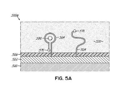
[0071] FIG. 5A is a schematic of a sensor device with a blocking layer having
anti-fouling
properties and a protective membrane layer.
[0072] FIG. 5B is a schematic of a sensor device with a blocking layer having
anti-fouling
properties and a protective membrane layer.
[0073] FIG. 5C is a schematic of a sensor device with a blocking layer having
anti-fouling
properties and a protective membrane layer.
[0074] FIG. 5D is a graph showing the performance of a cross-linked
polybetaine protective
membrane layer for fouling resistance in serum.
[0075] FIG. 6 is a schematic of a sensor device with a non-monolayer blocking
layer having anti-
fouling properties and a protective membrane layer.
DEFINITIONS
[0076] As used herein, "continuous sensing" with a "continuous sensor" means a
sensor that
changes in response to changing concentration of at least one solute in a
solution such as an analyte.
Similarly, as used herein, "continuous monitoring" means the capability of a
device to provide
multiple measurements of an analyte over time.
[0077] As used herein, the term "about," when referring to a value or to an
amount of mass, weight,
time, volume, pH, size, concentration or percentage is meant to encompass
variations of 20% in
some embodiments, 10% in some embodiments, 5% in some embodiments, 1% in
some
embodiments, 0.5% in some embodiments, and 0.1% in some embodiments from the
specified
amount, as such variations are appropriate to perform the disclosed method.
[0078] As used herein, the term "electrode" means any material that is
electrically conductive such
as gold, platinum, nickel, silicon, conductive liquid infused materials such
as ionic liquids,
PEDOT:PSS, conductive oxides, carbon, boron-doped diamond, nanotubes or
nanowire meshes,
or other suitable electrically conducting materials.
[0079] As used herein, the term -monolayer blocking layer" means a homogeneous
or
heterogeneous layer of material or of one or more types of molecules on an
electrode which reduce
- 15 -
CA 03232881 2024- 3- 22
WO 2023/049328
PCT/US2022/044512
electrochemical background current and/or current due to electrochemical
interference, and which
may promote proper freedom of movement for the aptamer which is required for
creating a
measurable response to analyte concentration.
[0080] As used herein, "monolayer blocking layer defect size" or "blocking
layer defect size" or
"blocking layer defect density" or "blocking layer fractional defect area" are
defined as used by
researchers who investigate the organization and defectivity of self-assembled
monolayers of
molecules on substrates such as gold. For avoidance of doubt, defect size and
defect density are
defined using the same measurement principles as taught in: Green, J.-B.D.,
Clarke, E., Porter,
M.D., McDermott, C.A., McDermott, M.T., Zhong, C.-J. and Bergren, A.J. (2022),
On the
Counter-Intuitive Heterogeneous Electron Transfer Barrier Properties of
Alkanethiolate
Monolayers on Gold: Smooth versus Rough Surfaces, Electroanalysis.
[0081] As used herein, the term "non-monolayer blocking layer" means a
homogeneous or
heterogeneous layer of material or of one or more types of molecules on an
electrode which do not
represent a monolayer configuration, and which reduces electrochemical
background current
and/or current due to electrochemical interference, and which may promote
proper freedom of
movement for the aptamer which is required for creating a measurable response
to analyte
concentration. For example, a metal or semiconductor oxide can be a non-
monolayer blocking
layer, or a thin polymer film may be a non-monolayer blocking layer, because
they are comprised
of multiple layers of atoms or molecules. A single atomic monolayer of SiO2
for example would
be a monolayer, whereas 3 nm of SiO2 is a non-monolayer.
[0082] As used herein, the term "antifouling layer" means a homogeneous or
heterogeneous layer
of material or of one or more types of molecules on a surface which reduces
fouling on a surface
compared to if such an antifouling layer was not utilized.
[0083] As used herein, the term "aptamer" means a molecule that undergoes a
conformation or
binding change as an analyte binds to the molecule, and which satisfies the
general operating
principles of the sensing method as described herein. Such molecules are,
e.g., natural or modified
DNA, RNA, or XNA oligonucleotide sequences, spiegelmers, peptide aptamers,
affimers and
other forms of affinity-based biosensors. Modifications may include
substituting unnatural nucleic
acid bases for natural bases within the aptamer sequence, replacing natural
sequences with
unnatural sequences, or other suitable modifications that improve sensor
function, but which
behave analogous to traditional aptamers. Two or more aptamers bound together
can also be
referred to as an aptamer (i.e., not separated in solution). Aptamers can have
molecular weights
of at least 1 kDa, 10 kDa, or 100 kDa.
[0084] As used herein, the term "redox tag" or "redox molecule- means any
species such as small
or large molecules with a redox active portion that when brought adjacent to
an electrode can
- 16 -
CA 03232881 2024- 3- 22
WO 2023/049328
PCT/US2022/044512
reversibly transfer at least one electron with the electrode. Redox tag or
molecule examples
include methylene blue. ferrocene, quinones, or other suitable species that
satisfy the definition of
a redox tag or molecule. In some cases, a redox tag or molecule is referred to
as a redox mediator.
Redox tags or molecules may also exchange electrons or change in behavior when
brought into
proximity with other redox tags or molecules. Exogenous redox molecules are
those added to a
device, e.g., they are not endogenous and provided by the sample fluid to be
tested.
[0085] As used herein, the term "change in electron transfer" means a redox
molecule whose
electron transfer with an electrode has changed in a measurable manner. This
change in electron
transfer call, for example, originate from availability for electron transfer,
distance from an
electrode, impedance between the redox molecule and the electrode, diffusion
rate to or from an
electrode, a shift or increase or decrease in electrochemical activity of the
redox molecule, or any
other embodiment as taught herein that results in a measurable change in
electron transfer between
the redox molecule and the electrode.
1100861 As used herein, the term "sensing monolayer" means at least a
plurality of aptamers on a
working electrode, which may also include a plurality of molecules or mixtures
of molecules that
form a blocking layer and/or an anti-fouling layer.
[0087] As used herein, the term "analyte- means any solute in a solution or
fluid which can be
measured using a sensor. Analytes can be small molecules, proteins, peptides,
electrolytes, acids,
bases, antibodies, molecules with small molecules bound to them, DNA, RNA,
drugs, chemicals,
pollutants, or other solutes in a solution or fluid.
[0088] As used herein, the term "continuous sensing" simply means the device
records a plurality
of readings over time.
[0089] As used herein, a "sensing device" or "device" comprises at least one
sensor based on at
least one aptamer and at least one sample solution. Devices can sense multiple
samples and be in
multiple configurations such as a device to measure a pin-prick of blood, or a
microneedle or in-
dwelling sensor needle to measure interstitial fluid, or a device to measure
saliva, tears, sweat, or
urine sensor, or a device to measure water pollutants or food processing
solutes, or other devices
which measure at least one analyte found in a sample solution.
[0090] As used herein, a "redox current" or "redox signal" comprises the total
redox current
between the plurality of redox tags attached to aptamers on the sensor and the
electrode for a given
sensor, the electrode typically referred to as the working electrode, as
measured using techniques
such as square voltammetry, chronoamperometry, or other suitable methods.
[0091] As used herein, "signal gain" comprises a change in the redox current
or signal due to a
change in concentration of the analyte as measured using techniques such as
square voltammetry,
chronoamperometry, or other suitable methods.
- 17 -
CA 03232881 2024- 3- 22
WO 2023/049328
PCT/US2022/044512
[0092] As used herein, "background current" comprises the current measured
that is not the redox
current. Background current can be due to capacitive charging, faradic
currents, oxygen reduction
currents, other redox active species, etc.
[0093] As used herein, a "sensor signal" or "normalized sensor signal"
comprises redox current
minus the background current which is normalized to the beginning of testing
of the sensor (such
as t=Os the sensor is placed into test solution such as serum). For example,
if the measurement is
a voltammogram from square wave voltammetry then than the sensor signal is the
peak height of
redox current as measured above the background current if there were no redox
tags.
[0094] As used herein, a "electron transfer rate" comprises the measured rate
or time at which
electrons are transferred between the redox tag and the working electrode.
[0095] As used herein, a "frequency response- refers to a change in signal
measured from the
device as a function of measurement frequency, such as the frequency used for
a square wave
voltammetry measurement. A change in frequency response can also be related to
a change in the
electron transfer rate.
[0096] As used herein, a "zero frequency" or "zero gain frequency" is a
measurement frequency
where the redox signal does not respond to an increase or decrease in
concentration of the analyte.
A zero gain frequency can be used to enable two frequency measurement which
then permits
calibration free operation.
[0097] As used herein, "sensor accuracy" is the maximum difference that will
exist between the
actual value (which must be measured by a primary or good secondary standard)
and the indicated
value at the output of the sensor. The accuracy can be expressed either as a
percentage of full scale
or in absolute terms.
[0098] As used herein, "test fluid" is interstitial fluid or a suitable proxy
for the test fluid such as
serum.
[0099] As used herein, a "protective membrane" refers to one or more layers or
materials which
protect a sensor blocking layer from fouling and is permeable to at least
electrical charge transfer.
A protective membrane may optionally also be selectively permeable to
additional components in
a test fluid such as, for example, at least one analyte, wherein the presence
of the at least one
analyte allows the sensor to operate properly while the protective membrane
protects against
performance reduction due to fouling, or some combination thereof.
DETAILED DESCRIPTION OF THE INVENTION
[0100] One or more specific embodiments of the present invention will be
described below. In an
effort to provide a concise description of these embodiments, all features of
an actual
implementation may not be described in the specification. It should be
appreciated that in the
- 18 -
CA 03232881 2024- 3- 22
WO 2023/049328
PCT/US2022/044512
development of any such actual implementation, as in any engineering or design
project, numerous
implementation-specific decisions must be made to achieve the developers'
specific goals, such as
compliance with system-related and business-related constraints, which may
vary from one
implementation to another. Moreover, it should be appreciated that such a
development effort
might be complex and time consuming, but would nevertheless be a routine
undertaking of design,
fabrication, and manufacture for those of ordinary skill having the benefit of
this disclosure.
[0101] Certain embodiments of the disclosed invention show sensors as simple
individual
elements. It is understood that many sensors require two or more electrodes,
reference electrodes,
or additional supporting technology or features which are not captured in the
description herein.
Sensors can be in duplicate, triplicate, or more, to provide improved data and
readings. Sensors
may provide continuous or discrete data and/or readings. Certain embodiments
of the disclosed
invention show sub-components of what would be sensing devices with more sub-
components
needed for use of the device in various applications, which are known (e.g., a
reference or counter
electrode, a battery, antenna, adhesive), and for purposes of brevity and
focus on inventive aspects,
such components may not be explicitly shown in the diagrams or described in
the embodiments of
the disclosed invention. All ranges of parameters disclosed herein include the
endpoints of the
ranges.
[0102] With reference to FIGS. lA and 1B, a conventional prior art sensor
device 100 is shown
placed in a sample fluid 130 such as interstitial fluid, comprising: at least
one working electrode
120 such as gold, carbon, or other suitable electrode material; at least one
monolayer blocking
layer 122 including a plurality of molecules such as, for example,
mercaptohexanol or hexanethiol
that are thiol bonded to the electrode, or a plurality of natural solutes in
blood such as, for example,
amino acids, peptides, albumin, etc. that can at least partially act as a
blocking layer, or other
suitable molecules depending on application and on the choice of electrode 120
material; at least
one aptamer 124 that is responsive to binding to an analyte 180 and which
contains a redox tag
170 such as, for example, methylene blue. In the generic example taught for
FIGS. 1A and 1B,
the aptamer 124 is a simple stem loop (hairpin) aptamer where analyte 180
binding causes the stem
loop to form and the redox current measured from the redox tag 170 to
increase, as measured using
square wave voltammetry, chronoamperometry, or some other suitable technique.
In absence of
analyte 180 binding to the aptamer 124 the stem loop conformation does not
form and the redox
current thus does not increase. Thus, changes in a measurement of redox
current can be used as a
signal to interpret changes in concentration of the analyte 180.
[0103] With further reference to FIG. 1B, a challenge with aptamer sensors is
that when placed
into initial operation the sample fluid 130, over a period of tens of minutes
to hours, the signal
(e.g., redox current) initially decreases by 30%, 50%, or even more, due to
effects such as fouling
- 19 -
CA 03232881 2024- 3- 22
WO 2023/049328
PCT/US2022/044512
by small molecules 186, proteins 188, or other solutes in the sample fluid
130, but also due to
desorption of the sensing monolayer, including aptamer 124 and/or blocking
layer 122. Various
aspects of the present invention aim to reduce or resolve entirely the amount
of initial or longer
term desorption, instability, and/or fouling of the sensing monolayer. During
fabrication of a
conventional aptamer sensor, a portion of the sensing monolayer is
physiosorbed to the electrode
120 surface, or molecules are incorrectly oriented (e.g., blocking layer that
is inverted with thiol
facing away from electrode 120), or there are portions of the electrode 120
that are physically or
electrochemically fragile, or other aspects of the sensing monolayer that can
readily detach from
the sensor during initial operation. Although one could just use an electronic
`burn-in' period to
stabilize the sensor when in initial use, the loss of aptamer 124 results in
an irrecoverable loss in
redox current from the sensor 100, and the loss of blocking layer 122 can
result in an increase in
background current and/or increased electrode 120 fouling. Furthermore, even
if the sensing
monolayer stays intact, if it exhibits significant fouling in a biofluid such
as interstitial fluid then
the redox current can decrease due to reduced electron transfer from the redox
tag 170 or reduced
freedom of movement for the aptamer 124 which can also reduce signal gain with
binding of the
analyte 180. Nuclease attack or methylation of the aptamer 124 are also
possible and will degrade
the signal from the sensor 120. The measurement of the sensor 100 can be
performed using one
of multiple techniques, such as chronoamperometry, square-wave voltammetry,
using one or more
calibration-free and/or drift correction methods, all of which are sensitive
to degradation of the
sensor 100. In summary, a non-limiting set of challenges may include the
following, which have
not been fully resolved by researchers in the field of aptamer sensors:
[0104] (1) Desorption of the aptamer from the sensing monolayer which reduces
the redox current,
and therefore sensor accuracy. Energetically stable aptamer attachment to the
working electrode
is preferred and is measurable by a stable sensor signal. When a sensing
monolayer is used, stable
aptamer attachment can have a strong dependence on the stability of the
monolayer blocking layer
that surrounds the aptamer.
[0105] (2) Desorption of blocking molecules from the sensing monolayer which
increases
background current due to increased electrical capacitance or interferents
such as oxygen reduction
current, and which changes electron-transfer rates between electrode and redox
tags thereby also
impacting redox current, signal gain, frequency response, and therefore sensor
accuracy.
Energetically stable blocking layer attachment to the working electrode is
preferred.
[0106] (3) Nuclease attack, oxidation, or methylation or other chemical attack
of the aptamer
which can sever the aptamer and release the redox tag and/or inhibit the
response of the aptamer
when it binds to analyte, all of which is resolvable or at least reducible by
modifying the aptamer
to be resistant to such attack.
- 20 -
CA 03232881 2024- 3- 22
WO 2023/049328
PCT/US2022/044512
[0107] (4) Fouling of the aptamer due to irreversible or frequent binding of a
solute to the aptamer
that is not the target analyte, which could alter or completely inhibit the
aptamer response to the
analyte.
[0108] (5) Fouling of the blocking layer which can alter the redox current,
signal gain, frequency
response, and/or rate of electron transfer by changing the electrical
impedance between the redox
tag and the electrode, and which can inhibit normal motion/response of the
aptamer to binding of
analyte to the aptamer, which further impacts signal gain and frequency
response. Fouling can
also accelerate desorption of the blocking molecules in the blocking layer by
creating intermediate
energy states that reduce the energy required for desorption of blocking
molecules. Reduced
fouling of the blocking layer is preferred.
[0109] (6) Fatigue of the redox tag where its reduction/oxidation becomes no
longer reversible,
shifted in potential, or some other change in the redox tag.
[0110] Of this list, changes in the aptamer (3), fouling of the aptamer (4),
and redox tag fatigue
(6) can be adequately insignificant during multi-day operation of a sensor
when using currently
available aptamers and redox tags such, for example, as methylene blue. For a
long-lasting sensor
that maintains sensor accuracy for multiple days such as, for example, at
least 3, 4, or 5 days, the
remaining list¨(1), (2), and (5)¨must be addressed in part and ideally in
whole, as will be further
taught for embodiments of the present invention. The present invention will
therefore be organized
into examples and embodiments that provide one or more of: (1) a stable sensor
signal; (2) an
energetically stable blocking layer; (5) resistance to fouling of the blocking
layer.
[0111] Several examples and embodiments of the present invention will now be
taught, and their
performance then subsequently summarized. As will be seen, several of the
examples are
surprising, revealing that previously-known short term fixes to improving
sensor longevity (over
hours) may actually increase sensing monolayer degradation in the longer term
(over days). For
example, it was previous thought that solutes in serum would stabilize a
sensing monolayer, which
may be true in the short term (hours) but is not true over periods of 3 days
or more, requiring an
alternate strategy for creating a stable sensor (for example, see "Achieving
Reproducible
Performance of Electrochemical, Folding Aptamer-Based Sensors on
Microelectrodes: Challenges
and Prospects- Anal. Chem. 2014, 86, 22, 11417-11424, October 22, 2014,
https://doi.org/10.1021/ac503407e). Furthermore, it has been observed that
electric field during
scanning of the sensors can energetically drive off the molecules in the
sensing monolayer and
therefore less frequent measurement may improve sensor longevity, which may be
true in the short
term (hours) but may not be true over periods of 3 days or more, where applied
electric field or
voltage can actually help further stabilize the sensing monolayer.
- 21 -
CA 03232881 2024- 3- 22
WO 2023/049328
PCT/US2022/044512
[0112] Unless specifically stated otherwise, examples using an aptamer
utilized the vancomycin
aptamer that is commonly reported in literature having the following
formulation: CGAGG
GTACC GCAAT AGTAC TTATT GTTCG CCTAT TGTGG GTCGG, with a carbon thiol linker
on the 5' end and methylene blue on the 3' end. This aptamer was chosen for
reproduction of
results. Embodiments of the invention may include other aptamers known to
persons having
ordinary skill in the art than those aptamers disclosed here, either as a
substitution for or in addition
to the vancomycin aptamer disclosed above.
[0113] For sensor fabrication, 2 mm diameter gold disk electrodes were used
and mechanically
roughened via abrasion or physical agitation in polishing slurries. The
working electrode was
further cleaned by running 700 cyclo-voltametric scans in 0.5 M NaOH from -1 V
to -1.6 V at a
scan rate of 1 V/s and subsequently 150 scans in 0.5 M H2SO4 solution by
scanning the potential
from 0 V to 1.6 V at 1 V/s. Once the electrochemical cleaning was completed,
electrodes were
thoroughly rinsed with DI water, dried in the nitrogen stream (99.999% purity)
and used for the
preparation of the sensors. Embodiments of the invention may include other
types of electrodes
such as, for example, gold wire, planar deposited gold, another suitable gold
working electrode,
and/or other types of working, counter, or reference electrode formulations,
so long as they satisfy
the sensor properties and performance as taught herein. Embodiments of the
invention may also
include electrodes having larger or smaller dimensions.
[0114] Unless specifically stated otherwise, the aptamers were bound to the
electrodes as follows.
First, a 100 i.t.M vancomycin aptamer stock solution was prepared in TE
buffer, including both
tris(hydroxymethyl)aminomethane (Tris) and ethylenediaminetetraacetic acid
(EDTA), and kept
at -20 C until used. The preparation of the aptamer solution for aptamer
incubation onto the
electrodes was performed by mixing an aliquot of the 100 p_M vancomycin stock
solution with
equal volume of the 0.5 M TCEP (tris(2-carboxyethyl)phosphine). The mixture
was allowed to
rest for lh, until the reduction of the thiolated aptamer was completed. The
obtained solution was
diluted to 500 nM with 1X phosphene buffered saline (PBS) with addition of 2
mM MgCl2 and
used for the functionalization of the gold-disk electrodes. A 20 1.t.1_,
droplet of the so-obtained
reduced aptamer solution was drop casted over the electrochemically cleaned
gold working
electrode surface and left to incubate for lh in a light-protected and
humidity-controlled chamber.
The aptamer functionalized electrodes were rinsed with DI water and incubated
for at least 12
hours in 5 mM solution of blocking layer molecules prepared in 1X PBS (buffer
solution). The
functionalized sensors were rinsed with DI water prior to measurement. In all
cases, purity of
solutions used during deposition are critical and otherwise will compromise
the sensor results, the
purity not being just the purchased purity but ensuring that all lab-ware and
solutions used are
clean and free from significant impurities that will compromise formation of a
stable sensing
- 22 -
CA 03232881 2024- 3- 22
WO 2023/049328
PCT/US2022/044512
monolayer. Generally, purity of solutions may have been discounted in prior
work because prior
work did not understand the mechanistic degradation mechanisms that result in
desorption of the
sensing monolayer.
[0115] All electrochemical measurements were performed by CH Instruments
galvanostat/potentiostat (Austin, Texas) connected to 64 channel multiplexers
in a standard three-
electrode system with the gold disk electrode serving as working electrode,
platinum counter
electrode and Ag/AgC1 (3 M KC1) reference electrodes tested under temperature
and humidity-
controlled conditions. Cyclic voltammograms were recorded in a potential
window from -0.1 V
to -0.5 V at a scan rate of 100 mV/s. For determining the electron-transfer
rate constant a set of
cyclic voltammograms was recorded at different scan rates ranging from 5 mV/s
to 100 V/s.
Square-wave voltammetry was performed in a potential window from -0.1 V to -
0.5 V at 25 mV
amplitude and unless otherwise specifically noted using a 300 Hz scanning
frequency. For the
longevity experiments, serum was spiked with sodium-azide to a final
concentration of 0.02% wt.
to prevent growth of microorganisms. Averaged sensor measurements were
performed across 4
sensors for each sensor type, and in comparative tests there were 4 sensors
and 2 types for 8 total
electrodes such that cycling through each electrode occurred approximately
every 30s, during
which each electrode experienced voltage for approximately 2s to complete the
scan on each
electrode.
EXAMPLES
Example 1: Biosensor including a Stable Sensor Signal, and an Energetically
Stable Blocking
Layer, but no Fouling Resistance.
[0116] With reference to FIG. 2, an example of a conventional sensor using a
hexane- thiol
blocking layer is shown to be inadequate at least because it experiences
sensor signal degradation
over time. Hexane-thiol provides stability in background current because the
hexane-thiol is
energetically more stable on the gold working electrode, but suffers from
significant fouling of the
blocking layer due to the hydrophobicity at the terminus of the hexane-thiol
molecules (the
terminus end faces the solution or sample fluid). The abrupt drop in sensor
signal for electrode 1
(El), electrode 2 (E2), and electrode 3 (E3) occurs when the sensors are
placed into a sample fluid
of serum. The sensor signal decrease rapidly occurs over 1-2 hours and is
approximately an 80%
loss of signal due to rapid fouling of the blocking layer in serum which
decreases the redox current.
Common foulants include albumin, which has hydrophobicity which easily adheres
to the
hydrophobicity of hexane-thiol blocking layer. The sensors also rapidly
decrease in signal gain
(not shown), to a level of poor performance, because the fouling is so strong
that a build up of
proteins like albumin will actually restrict freedom of movement of the
aptamers. Therefore, while
providing energetic stability for the blocking layer, this example is not a
viable solution for a sensor
- 23 -
CA 03232881 2024- 3- 22
WO 2023/049328
PCT/US2022/044512
with long-lasting signal gain and sensor accuracy. The strong fouling of the
sensors in FIG. 2
occurred across aptamers tested for analytes such as phenylalanine,
vancomycin, and cortisol,
confirming that the reduction in sensor performance is due to fouling of the
blocking layer.
[0117] The following examples describe and build on aspects of the present
invention. Aspects
of the present invention may be used together or in isolation (for example and
antifouling blocking
layer and/or a protective hydrogel against fouling). Therefore, each example
need not explicitly
teach all such uses of aspects of the present invention when used together or
in isolation.
Example 2: Biosensor including Stable Sensor Signal, Energetically Stable
Blocking Layer, and
Moderate Fouling Resistance.
[0118] With reference to FIG. 3, where like numerals refer to like components
of FIG. 1A unless
specified otherwise, an embodiment of a sensor device 300 in accordance with
the principles of
the present invention is shown. The sensor device 300 includes at least one
working electrode
320, at least one blocking layer 322, at least one aptamer 324 that is
responsive to binding to an
analyte 380 and which contains a redox tag 370. In one embodiment, the at
least one working
electrode 320 includes a material selected from the group consisting of gold,
carbon, or another
suitable electrode material. In one embodiment, the at least one aptamer 324
is the vancomycin
aptamer which, like other possible aptamers, can be used to implement
electrochemical
measurement techniques such as, for example, square wave voltammetry,
chronoamperometry, or
some other suitable technique. In such an embodiment, the absence of the
analyte 380 binding to
the aptamer 324 results in in a decrease in redox current. The sensor device
300 differs from the
conventional sensor device 100 at least because of the differences between the
composition of the
blocking layer 122 and the composition of the blocking layer 322. In one
embodiment, the
blocking layer 322 imparts a fouling resistance to the sensor device 300. In
another embodiment,
the blocking layer 322 is stable for greater than or equal to 3 days, more
preferably stable for
greater than or equal to 5 days at a temperature greater than or equal to 30
C. In a further
embodiment, the blocking layer 322 is stable for greater than or equal to 3
days, more preferably
stable for greater than or equal to 5 days at a temperature greater than or
equal to 30 C and less
than or equal to 47 C. In a further embodiment, the blocking layer 322
includes a plurality of
molecules that impart a fouling resistance and longevity to the sensor device
300 such as, for
example, mercaptooctanol (MCO) or other suitable alkylthiols or blocking
molecules having a
binding energy on rough gold that inhibits significant desorption of the
blocking layer for at least
3 days at a temperature greater than or equal to 30 C. In a further
embodiment, the blocking layer
322 includes a plurality of molecules that impart fouling resistance and
longevity to the sensor
device 300 such as, for example, MCO or other suitable alkylthiols or blocking
molecules having
- 24 -
CA 03232881 2024- 3- 22
WO 2023/049328
PCT/US2022/044512
a binding energy on rough gold that inhibits significant desorption of the
blocking layer at a
temperature greater than or equal to 30 C and less than or equal to 47 C.
[0119] With reference to FIGS. 3A, 3B, and embodiments of the present
invention, data is shown
for a vancomycin sensing device that has a stable sensor signal, energetically
stable blocking layer,
and moderate fouling resistance. The results for a mercaptooctanol (MCO)
blocking layer are
shown on mechanically polished gold disks of 2 mm diameter and compared to a
much less stable
mercaptohexanol (MCH) blocking layer fabricated in the same manner as the MCO.
Both the
sensors and blocking layers of MCH and MCO were fabricated identically except
for the chemical
composition associated with MCH vs. MCO. With further reference to FIG. 3A,
3B, the sensors
are repeatedly scanned with square wave voltammetry during data collection.
The sensors are
tested in serum at 37 C in order to test against stable sensor signal, an
energetically stable blocking
layer, and resistance to fouling.
[0120] The plots measure sensor signal vs. time for multiple sensors and
include standard
deviation for the sensor signal (gray shading outside the sensor colored raw
redox current data).
The MCO scnsor exhibits superior longevity as indicated by greater than or
equal to 50% of sensor
signal remaining for a period of time greater than or equal to 3, 4, or 5 days
of operation at a
temperature of 37 C, which is significantly greater than a typical lower limit
for a dermal
indwelling sensor of greater than or equal to 30 C. The MCH layer sensor
signal is less stable as
indicated by the measured increase in signal, which is evidence of sensor
degradation as will be
discussed in more detail below with regard to FIG. 3C. The MCO layer still has
an initial fouling
response resulting in 50% sensor signal loss which is similar to that shown
for MCH as well, but
which is superior to the ¨80% sensor signal loss due to fouling of the
hexanethiol monolayer
blocking layer of FIG. 2. The MCO blocking layer is energetically more stable
due to a greater
energy needed for desorption from the monolayer, achieved by a longer
hydrophobic chain (8 vs.
6 carbons) compared to commonly used MCH blocking layers. The thiol¨gold bond
can be
described as a surface-bound thiolate. The gold¨thiolate bond energy is
approximately only 170
kJ/mol due to the polar nature of the bond, causing it to be regarded as a
pseudo-covalent bond.
Van der Waals forces between neighboring molecules stabilize the structure
further with a greater
total binding energy. For alkythiols on 111 oriented gold, the total binding
energy of MCH is -
2.98 eV whereas the total binding energy of MCO is -3.17. This small binding
energy increase
for MCO is significant, as predicted by the Arrhenius equation, k=Ae^(-E/RT),
where E is the
binding energy. The binding energy difference between -2.98 eV and -3.17 eV is
significant
enough to raise a maximum stable temperature of the sensor by nearly 20 C (or
Kelvin), which
explains both why MCH can be shown to be stable for several days at room
temperature but is
instable at greater than or equal to 30 C and why MCO is highly stable even at
temperatures greater
- 25 -
CA 03232881 2024- 3- 22
WO 2023/049328
PCT/US2022/044512
than or equal to 30 C. These total binding energy stabilities are further
dependent on an underlying
gold surface with optimal roughness and crystallinity, as will be taught later
as part of
embodiments of the present invention. In one embodiment, molecules in the
blocking monolayer
of the present invention may include those having a total binding energy of
that is equal to or more
negative than -3.00 eV, more preferably still equal to or more negative than -
3.05 eV, and even
more preferably equal to or more negative than -3.1 eV.
[0121] With further reference to FIG. 3B, 50 mIVI Ethylenediaminetetraacetic
acid (EDTA) was
added to confirm that nuclease attack was not causing the degradation. In
FIGS. 3B, 3C and 3D
the signal and the voltammograms for MCH and MCO respectively are shown at 1,
3, 5, 7, and 9
days. These graphs confirm, that even in the presence of 50 mM EDTA, the MCH
blocking layer
is unstable past 3 days as increased background accelerates after 3 days due
to both increased
capacitive charging and increased oxygen reduction current (which occurs at
larger negative
voltages). The MCO electrode is stable for greater than one week even at 37 C
and in serum.
Referring back to Fig. 3A, which is without added EDTA and therefore more
representative of a
natural biofluid such as interstitial fluid, the device with the MCH blocking
layer begins to fail
after only 36 hours, which is far short of 3 days, while the MCO blocking
layer remains stable for
at least 3, 4, or 5 days.
[0122] The results in FIGS. 3A-3D only partially resolve all the ideal
performance metrics for a
long-lasting stable sensor because sensor signal is not the only metric that
matters. For example,
as shown in FIGS. 4A and 4B, the signal gain in response to vancomycin
decreases significantly
after 3 days for the same sensors due to partial fouling of the MCO blocking
layer surface. For
example, after 3 days of continuous scanning in a 20011M MCO solution at 37 C,
the signal gain
of the sensor decreased from about 80% to about 25% (approximately 4 times), a
decrease of less
than four times of its original value (i.e., preserves greater than one fourth
of its original signal
gain value). This 25% signal gain still permits an accurate reading using two-
frequency calibration
free measurements but has reduced accuracy due to weaker signal gain and a
shift in the sensor
frequency response. This continued loss in signal gain and shift in frequency
response is due to
fouling of the MCO layer which inhibits or alters electron transfer and/or
freedom of movement
for the aptamer. Both fouling and monolayer passivation have a strong
dependency on feature
types and densities of the monolayer, which will be discussed next for
embodiments of the present
invention.
Example 3: Electrode Roughness And Monolayer Blocking Layer Defects For Stable
Sensor
Signal, Energetically Stable Blocking Layer, And Fouling Resistance
[0123] With reference to embodiments of the present invention, not only does
the choice of
blocking layer effect sensor signal stability and fouling resistance, but
sensor signal stability and
- 26 -
CA 03232881 2024- 3- 22
WO 2023/049328
PCT/US2022/044512
fouling resistance can both be strongly affected by the underlying electrode
crystallinity and
roughness. For example, a perfectly planar or highly crystalline gold
electrode can actually bias
the size distribution of features in the blocking monolayer toward features
that are larger in size,
resulting in a less energetically stable blocking layer than a blocking layer
formed on rougher gold,
which has smaller sized and more energetically stable defects due, at least in
part, to the step edges
in rougher gold. Furthermore, the right density of features can be beneficial
as features promote
electron transfer between the redox tag and the working electrode as explained
further below in
the discussion of defects. Features can include, for example, defects in the
blocking layer,
electrically conductive molecules, pores, other suitable means of promoting
electron transfer, or
combinations thereof. With respect to defects, larger defects can also act as
sites where undesirable
fouling nucleates more quickly. Therefore, an optimum surface density and size
of monolayer
defects is desired, all of which is affected by electrode crystallinity and
roughness. For example,
to ensure that an adequate density of blocking layer defects occur at step
edges of a gold surface,
the gold may have a roughness that has at least 1 's or 10's of nm changes in
height of the gold
over distances of 10's to 100's of nm in the perpendicular plane (i.e., the
width). This roughness
of the gold can be expressed using average roughness slope, which is a ratio
between the change
in step height over a given width. For example, gold that has a 1 nm change in
step height
(tangential to the local surface or radii of curvature) over 10 nm of width of
planar gold domain
has a 10% average roughness slope to it. Therefore, an embodiment of the
present invention may
utilize gold with an average slope roughness of less than or equal to at least
one of 0.5%, 1%, 2%,
5%, 10%, 20%, or 50%. Roughness of the electrode may be at least partially
dependent on the
stability of the electrode material. For example, a conventional
electrochemically roughened gold
electrode may exhibit mechanically, thermally, and chemically unstable
features such as nano-
scale gold dendrites, nano-porous structures, other unstable features, or some
combination thereof.
For example, nano-porous gold has a roughness and porosity that can change
over time (decrease)
even at room or body temperature as the gold self-anneals and changes in
geometry over time. In
one embodiment, the gold electrode may have an average slope roughness of less
than or equal to
at least one of 0.5%, 1%, 2%, 5%, 10%, 20%, or 50% after annealing of unstable
features. In
another embodiment, the gold electrode may have an average slope roughness of
less than or equal
to at least one of 0.5%, 1%, 2%, 5%. 10%, 20%, or 50% before annealing of
unstable features.
[0124] With further reference to embodiments of the present invention, a
perfectly defect-free
blocking layer with little or no tunneling current could make for a poor
biosensor because, for
example, electron transfer with the redox-tag could be inhibited and/or
electron transfer kinetics
could be too slow and therefore limit the availability of a zero gain
frequency. Conversely, a too
highly defective blocking layer would have too much background current from
capacitive charging
- 27 -
CA 03232881 2024- 3- 22
WO 2023/049328
PCT/US2022/044512
from molecular interferents in the sample fluid and/or due to oxygen reduction
current. Therefore,
a balance or goldilocks' zone for the right density and size of monolayer
blocking layer defects
is preferred. The size and density of defects in the blocking layer can be
determined using a
measurement technique such as, for example, an optical method, AFM, scanning
tunneling
microscopy, or other suitable measurement techniques. In a preferred
embodiment, the majority
of blocking layer defect sizes may be less than or equal to 0.3 nm in size. In
various embodiments,
the blocking layer has defects with a fractional area of the total surface
area that is, in various
embodiments, less than 0.2, less than 0.1, less than 0.05, or even less than
0.02. In various
embodiments, layer 122 has defects that have a fractional area of the total
surface area that is, in
various embodiments, at least greater than 0.001, greater than 0.002, greater
than 0.005, greater
than 0.01. The defect size is typically measured as a width of a defect
between adjacent ordered
domains of the blocking layer molecules and in an image of the scan appears as
a void or crack in
between adjacent ordered domains of the blocking layer molecules. A smaller
defect size promotes
energetic stability of the monolayer at least because blocking layer molecules
that have a
hydrophobic interior region, such as alkythiols, experience a local energy
minima when they arc
tightly packed (i.e., surrounded) with similar blocking layer molecules (i.e.,
it is more difficult to
desorb a blocking layer molecule from such a layer). In one embodiment, the
blocking layer has
a fractional defect area, which is a measure of the area of the underlying
electrode that is exposed
by the defects as a fraction of total electrode area. In some embodiments, the
fractional defect area
may be at least 0.01 for the majority of the defect sizes. The blocking layer
defect sizes and
densities can be controlled by the roughness and crystallinity of the
electrode. As an example, two
extremes of such roughness and crystallinity control can be achieved for
example by sputtering or
evaporating an electrode such as gold a rate of greater than or equal to 10
nm/min to create very
rough electrodes with a high density of small defects (less than or equal to
0.3 nm), to instead
annealing of gold electrodes at 400-500 C for several hours to smoothen and
crystalize the
electrode surface and result in a high density of large defects such as, for
example, greater than or
equal to 0.3 nm.
Example 4: Stable Sensor Signal, Energetically Stable Blocking Layer, and
Strong Fouling
Resistance via Addition of a Protective Membrane
[01251 With reference to FIGS. 5A-5C, where like numerals refer to like
features shown and
described in FIGS. 1 and 3, a protective membrane layer 526 may be added to
the device 500a,
500b, or 500c. With reference to FIG. 5A, the device 500a includes the
protective membrane layer
526 may be positioned above the blocking layer 522. In one embodiment, the
protective membrane
layer 526 may be positioned such that a majority of the protective membrane
layer 526 covers and
is in contact with a majority of blocking layer 522. In such embodiments, if
the protective
- 28 -
CA 03232881 2024- 3- 22
WO 2023/049328
PCT/US2022/044512
membrane is so dense that it can block free motion of the aptamer 524, then
the thickness of the
protective membrane layer 526 may be inversely correlated with electron
transfer of the device
500a and the membrane 526 may be less than or equal to 10 nm, less than or
equal to 5 nm, and
even more preferably less than or equal to 1 nm, such as being an ultrathin
antifouling layer of a
glycol or monolayer of a zwitter ion moiety. If the protective membrane 526
does not block free
motion of the aptamer 524 such as being a semiporous hydrogel in which the
aptamer can freely
move, then the thickness of the protective membrane 526 may be less than or
equal to 1 mm, more
preferably less than or equal to 100 microns, and even more preferably less
than or equal to 10
microns. The protective membrane may be for example a hydrogel such as a
solution of betaine
that is solution cast onto to the blocking layer 522 and then crosslinked
chemically or with ultra-
violet light to form a polybetaine protective hydrogel.
[0126] With reference to FIG. 5B, a device 500b in accordance with principles
of the present
invention is shown. As shown, the protective membrane layer 526 may be
attached at or around
an outer perimeter 528 as shown. Although the outer perimeter 528 is shown to
be at or near an
edge of the electrode 520, the outer perimeter 528 may encompass the electrode
520 without
contacting the electrode 520 (not shown). In one embodiment, the protective
membrane layer 526
forms an enclosed space 550 above the blocking layer 522 and encompasses the
blocking layer
522 such that any sample fluid such as a test fluid 530 comes in contact with
the protective
membrane layer 526 before the aptamer 524. In one embodiment, the test fluid
530 is filtered
through the protective membrane layer 526 as it enters the enclosed space 550,
removing at least
one solute present in the test fluid 530, to define a filtered test fluid 532
as shown. The at least
one solute filtered out by the protective membrane 526 to define the filtered
test fluid 532 may be,
for example, albumin, while the analyte such as vancomycin may freely exchange
between test
fluid 530 and filtered test fluid 532. In one embodiment, the enclosed space
550 is sized so that
the at least one aptamer 524 is separated from contact with the protective
membrane layer 526. In
one embodiment, at least one of the height of the protective membrane layer
526 and the maximum
height of the protective membrane 526 is selected to minimize contact between
the aptamer 524
and the protective membrane 526.
[0127] With reference to FIG. 5C, a device 500c in accordance with principles
of the present
invention is shown. As shown, the outer perimeter 528 is a raised perimeter
528 having a top
surface 529 on which the protective membrane layer 526 is applied. Although
the raised perimeter
528 is shown to be at or near an edge of the electrode 520, the raised
perimeter 528 may encompass
the electrode 520 without contacting the electrode 520 (not shown). In one
embodiment, the test
fluid 530 is filtered through the protective membrane layer 526 as it enters
the enclosed space 550,
removing at least one solute present in the test fluid 530, to define a
filtered test fluid 532 as shown.
- 29 -
CA 03232881 2024- 3- 22
WO 2023/049328
PCT/US2022/044512
The at least one solute filtered out by the protective membrane 526 to define
the filtered test fluid
532 may be, for example, albumin, while the analyte such as vancomycin may
freely exchange
between test fluid 530 and filtered test fluid 532. The raised perimeter 528
may be impermeable
to fluids such as, for example, the test fluid 530, the interstitial fluid, or
serum. In one embodiment,
the raised perimeter 528 and the protective membrane layer 526 form an
enclosed space 550 above
the blocking layer 522. In one embodiment, the raised perimeter 528 may have a
height between
the top portion 529 and the blocking layer 522 greater than the height of the
aptamer 524 such that
the protective membrane layer 526 is separated from the aptamer 524. In one
embodiment, the
enclosed space 550 is sized so that the at least one aptamer 524 is separated
from contact with the
protective membrane layer 526.
[0128] With reference to FIGS. 5B and 5C, the perimeter 528 may have a cross
section
perpendicular to the height that defines a perimeter shape. The perimeter
shape may be polygonal
such as, for example, a triangle, a square, a rectangle, a rhombus, a hexagon,
an octagon, or other
suitable polygonal shapes_ The perimeter shape may have one or more rounded
edges such as, for
example, a circle, a semi-circle, or a modified polygon with curved edges.
Similarly, the electrode
520 may have a cross section perpendicular to the height that defines an
electrode shape. The
electrode shape may be polygonal such as, for example, a triangle, a square, a
rectangle, a rhombus,
a hexagon, an octagon, or other suitable polygonal shapes. The electrode shape
may have one or
more rounded edges such as, for example, a circle, a semi-circle, or a
modified polygon with
curved edges. In one embodiment, the perimeter shape is selected to match the
electrode shape.
With further reference to embodiments of the present invention alternate
membrane geometries
are possible. For example, if a gold-wire working electrode was utilized, the
protective membrane
may be a dialysis tube into which the gold wire is inserted (not shown).
[0129] With reference to FIGS. 5A-5C, the protective membrane layer 526 may be
adhered to the
blocking layer 522 and/or the perimeter 528 by attachment methods such as, for
example,
chemically bonding the protective membrane layer 526 to the blocking layer 522
and/or the
perimeter 528, mechanically adhering the protective membrane layer 526 to the
blocking layer 522
and/or the perimeter 528, applying an adhesive at least at a point of contact
between the protective
membrane layer 526 and the blocking layer 522 and/or the perimeter 528, some
other suitable
methods of adhering two surfaces together, or some combination thereof. In one
embodiment, the
protective membrane layer 526 is partially protective against fouling. A
protective membrane
layer 526 may include a polymer material such as, for example, polybetaine,
polyurethane,
polyvinylpyridin, polyvinylimidazole, or some other suitable polymer. In a
further embodiment,
the protective membrane layer 526 is crosslinked using a method such as, but
not limited to, using
a crosslinking agent, applying UV radiation, using another suitable cross-
linking method, or some
- 30 -
CA 03232881 2024- 3- 22
WO 2023/049328
PCT/US2022/044512
combination thereof. In one embodiment, the protective membrane layer 526 is a
thin film that is
applied on top of a device 500. In a further embodiment, the thin film
protective membrane layer
526 has a thickness less than or equal to 1 mm, more preferably less than or
equal to 100 microns,
and even more preferably less than or equal to 10 microns. In another example,
polybetaine may
be used in a protective membrane layer 526 that can be coated onto the
blocking layer 522 as a
solution, and cross-linked with UV light such that is forms a protective
membrane layer 526 that
is adhered chemically, mechanically, or through other forces at least in part
to the surface formed
by blocking layer 522 and aptamers 524.
[0130] With reference to FIG. 5D for a vancomycin sensing device and with
reference to
embodiments of the present invention, a stable sensor signal, energetically
stable blocking layer,
and fouling resistance are achieved using a monolayer blocking layer such as
MCO and a hydrogel
protective membrane layer on the MCO electrode such as UV-cross-linked
polybetaine onto the
working electrode, or alternately, polyurethane, polyvinylpyridin or
polyvinylimidazole or other
membranes. The device also used a porous gold electrode to increase adhesion
of the hydrogel on
the working electrode, the porous gold formed by repeated electrochemical
alloying/dealloying
(6000 cycles). The porous gold clearly increases the initial electrode fouling
response with greater
than or equal to 80% sensor signal loss when tested in serum at 37 C without
membrane protection.
This increased fouling may be due to a rougher gold surface having a greater
density of blocking
layer defects which in turn act as nucleation sites for electrode fouling (as
discussed above).
Importantly, with addition of the cross-linked polybetaine the fouling is
strongly prevented,
preserving greater than or equal to 90% of the sensor signal and greater than
or equal to 90% of
the signal gain initially during the first 2 hours of operation. Optimization
of the hydrogel and
sensor can preserve at least one of at least greater than or equal to 50% and
greater than or equal
to 80% of the sensor signal and signal gain for at least one of 3, 4, or 5
days, including formation
on gold with reduced porosity and therefore reduced blocking layer defect
density. For example,
tests with MCO and UV-cross-linked polybetaine and after 3 days of testing at
37 C in serum
results in a signal gain of 105% at 750 IuM vancomycin at day 0 and 102% at
750 litM vancomycin
at day 3, showing very little loss in signal gain (no significant change
within the standard deviation
of +/-7%) and no significant change in sensor signal (redox peak current)
within the standard
deviation. In a preferred embodiment, the sensor provides at least one of less
than 30, 20, 10, 5%
loss in signal gain after 3 days of operation at greater than or equal to 30 C
in a biofluid such as
serum or interstitial fluid. Such longevity of performance is enabled by use
of the more
energetically stable MCO blocking layer and an optimal gold surface and
roughness which
otherwise would not be achievable with a blocking layer such as MCH.
Furthermore, because the
monolayer blocking layer is stable and because robust resistance to fouling is
achieved, the
- 31 -
CA 03232881 2024- 3- 22
WO 2023/049328
PCT/US2022/044512
electron transfer rates and freedom of movement for the aptamer are preserved,
and therefore the
frequency response is preserved. Frequency response is heavily dependent on
aptamer. In the test
shown in FIG. 5D, the vancomycin aptamer was used. However, other aptamers
could be used in
accordance with the principles of this invention such as, for example, those
demonstrated for
phenyl al anine, cortisol , dox orubici n, irinotecan, or other aptamers. The
zero frequency response
may shift after 3 days in a biofluid such as, for example, a serum or
interstitial fluid by at least one
of less than or equal to 5%, less than or equal to 10%, less than or equal to
20, less than or equal
to 40, less than or equal to 80%. In one non-limiting example, the zero
frequency response for a
vancomycin aptamer shifted from 30 Hz to 36 Hz after 3 days (20%). Embodiments
of the present
invention therefore enable a stable frequency response for zero frequency or
for some other
measurable signal gain (e.g., 20% gain for 5-501.1.M analyte increase).
Embodiments of the present
invention therefore enable a signal gain that decreases by less than or equal
to 2 times, less than or
equal to 1.5 times, less than or equal to 1.2 times the original value of the
signal gain for at least
one of 3, 4, or even 5 days (i.e., would preserve a percentage of the original
signal gain greater
than or equal to 50%, greater than or equal to 67%, or greater than or equal
to 83% of the original
total signal gain) at greater than or equal to 30 C in a biofluid such as
serum or interstitial fluid.
[0131] With further reference to the present invention, adequate electron
transfer then allows for
adequate sensor signal at lower square-wave- voltammetry measurement
frequencies such that two
frequency or similar auto-calibration (calibration free) methods are still
possible because a zero-
gain frequency that is measurable exists for the sensor. In one embodiment,
the sensor may have
a zero-gain frequency greater than or equal to 2 Hz, greater than or equal to
5 Hz, greater than or
equal to 10 Hz, greater than or equal to 20 Hz, greater than or equal to 50
Hz, or greater than or
equal to 100 Hz at greater than or equal to 30 C in a biofluid such as serum
or interstitial fluid,
depending on blocking-layer configuration. The zero gain frequency of the
tested aptamer may
depend on variables such as, for example, thickness of the blocking layer 522,
number of defects
in the blocking layer 522, and density of defects in the blocking layer 522.
For example, if the
blocking layer is made too thick or is made with an inadequate amount or
density of defects, then
the zero gain frequency of the sensor could be at a frequency below 2 Hz which
makes accurate
measurement more difficult due to a weaker redox current measurement during
square wave
voltammetry. In one embodiment, the thickness of the blocking layer 522 is
less than or equal to
nm, more preferably less than or equal to 5 nm, even more preferably less than
or equal to 100
A , and still more preferably less than or equal to 10 A . In one embodiment,
the amount and
density of defects is primarily determined by selecting an average slope
roughness of the electrode
522 as discussed above. In a further embodiment, the average slope roughness
may be less than
or equal to at least one of 0.5%, 1%, 2%, 5%, 10%, 20% and 40%. The zero gain
frequency of the
- 32 -
CA 03232881 2024- 3- 22
WO 2023/049328
PCT/US2022/044512
sensor may also change over time due to factors such as, for example,
desorption of at least part
of the blocking layer 522, desorption of at least all or some of the at least
one aptamer 524, or
some combination thereof. In one embodiment, the sensor may exhibit a daily
change in zero-
gain frequency selected from the group consisting of less than or equal to
10%, less than or equal
to 5%, and less than or equal to 2% per day.
Example 5: Stable Sensor Signal, Energetically Stable Blocking Layer, and
Strong Fouling
Resistance via the Surface of the Blocking Layer
[0132] With reference to embodiments of the present invention, a stable sensor
signal,
energetically stable blocking layer, and strong fouling resistance can be
achieved using a
monolayer blocking layer that is modified with a highly hydrophilic terminal
moiety such as a
zwitterionic group, polyethylene glycol group, or other suitable anti-fouling
group that is highly
hydrophilic (e.g., a functional group that creates a layer of bound or
adjacent water that repels
foulant molecules). Preferably the end-group is a distal moiety with a smaller
size than the
footprint of the alkyl chain to prevent additional energetically unstable
defects from being formed
in the self-assembled monolayer, and therefore the moiety occupies a width
that at least one of less
than or equal to 10 A', one of less than or equal to 20 A', or less than or
equal to 30 A', or less
than or equal to 50 A . Another way to specify at preferred size restriction
for the distal moieties
is that the monolayer of blocking molecules is able to self-assemble in defect-
free ordered groups
(i.e., a two-dimensional domain) containing at least on average 10 blocking
molecules, or at least
on average 20 blocking molecules, or more preferably containing at least on
average 50 blocking
molecules. Preferably such a monolayer blocking layer formed of such molecules
provides a
fouling resistance of at least one of less than or equal to 5%, less than or
equal to 10%, less than
or equal to 20%, less than or equal to 40% loss in sensor signal after a time
greater than or equal
to 3, 4, 5, or more days of operation at a temperature of 37 C, which is
significantly greater than
a lower limit for a dermal indwelling sensor of greater than or equal to 30 C.
The zero frequency
response may shift by at least one of less than or equal to 5%, less than or
equal to 10%, less than
or equal to 20%, less than or equal to 40%, or less than or equal to 80% after
a time greater than
or equal to 3 days. For example, a vancomycin aptamer only had a zero
frequency response shift
from 30 Hz to 36 Hz after 3 days (20%). Embodiments of the present invention
therefore enable
a signal gain that decreases by less than or equal to 2 times, less than or
equal to 1.5 times, or less
than or equal to 1.2 times the original value of the signal gain for at least
one of 3, 4, or even 5
days (i.e., the sensor would preserve greater than or equal to 50%, greater
than or equal to 67%,
and greater than or equal to 83% of the original total signal gain) at greater
than or equal to 30 C
in a biofluid such as serum or interstitial fluid. Preferably each molecule in
the blocking monolayer
- 33 -
CA 03232881 2024- 3- 22
WO 2023/049328
PCT/US2022/044512
has binding energy that is equal to or more negative than -3.00 eV, or more
preferably equal to or
more negative than -3.1 eV.
[0133] While blocking molecules having an alkyl chain are discussed above,
embodiments of the
invention may include other polymer chains such as, for example, a polyalkene
chain
¨(CH=CH).¨, a polyethylene glycol chain ¨(CH2CH20).¨, a polypropylene chain
¨(CH2CMeH),¨, or other suitable polymer chains. In one embodiment, the type of
polymer chain
for the blocking layer molecules is selected based on length of the carbon
chain. For example, if
the length of the polymer chain is excessive, then electrical response may be
undesirably reduced.
In one embodiment, for example, blocking layer molecules haying, cumulatively
in total carbon
chain links, an 8, 10, or 12 carbon chain length terminated with
phosphatidylcholine may achieve
such performance. The assembly of such monolayers may require tight control of
the buffer
conditions used and may also be aptamer dependent as interactions between the
aptamer and or
the blocking layer molecules with the blocking layer molecules themselves can
strongly impact
the quality of the formed sensing monolayer. In another embodiment, the type
of polymer chain
is selected based on the width of the polymer chain. For example, if the width
of the polymer
chain is excessive, then bigger gaps between blocking layer molecules (i.e.,
defects in the blocking
layer) may result in solutes reaching the electrode and causing increased
oxygen reduction current
or increased fouling. In one embodiment, for example, the type of polymer
chain is selected so
that the width is less than or equal to 50 A , more preferably less than or
equal to 30 A , more
preferably less than or equal to 20 A , and even more preferably less than or
equal to 10 A .
[0134] With reference to FIG. 6, where like numerals refer to like features
shown and described
in FIGS. 1, 3 and 5, an anti-fouling layer 626 may be added to a non-monolayer
blocking layer
622. In one embodiment, the non-monolayer blocking layer 622 may include a
material where the
molecules in the blocking layer are chemically bonded to each other, such as,
for example, silicon
dioxide (SiO2), titanium oxide (TiO2). or other metal or semiconductor oxides
with defects such
as porosities that mimic the electrochemical performance of monolayer blocking
layers as taught
herein. As shown in FIG. 6, the anti-fouling layer 626 covers a majority of
the non-monolayer
blocking layer 622. In one example, non-monolayer blocking layer 622 can be a
material with a
negatively charged or hydrophilic end group such as, for example, a zwitter
ion, polyethyelene
glycol, oligo(ethylene glycol), or another suitable end-group that repels
foulants and/or protects
pores or defects in non-monolayer blocking layer 622 from solutes in fluid
630. In another
example, anti-fouling layer 626 could be a self-assembled monolayer of
molecules having a
molecular structure such as, for example, of R1¨(CI-12).¨R7, where Ri is a
headgroup that prevents
fouling, ¨(CH2)a¨ is a nonpolar alkane chain, and R2 is an anchoring group
that is chemically
attached to at least one substrate including the non-monolayer blocking layer
622 and/or the
- 34 -
CA 03232881 2024- 3- 22
WO 2023/049328
PCT/US2022/044512
electrode 620. In one embodiment, the head group may be selected for anti-
fouling properties. In
a further embodiment, the hydrophilic properties of the head group may help
prevent or reduce
fouling. In one embodiment, the head group may be selected from the group
consisting of a
hydroxyl group, a zwitterionic group, a polyethylene group, phosphatidycholine
group, or other
suitable hydrophilic modifiers. In one embodiment, the non-polar alkane chain
may be replaced
with another polymer chain such as, for example, a polyalkene chain
¨(CH=CH)õ¨, a polyethylene
glycol chain ¨(CH7CH10)11¨, a polypropylene chain ¨(CH2CMeH)11¨, or other
suitable polymer
chains. For different substrates, the selection of the anchoring group, R2,
will be different: a silane
(¨SiC13) anchor group may be used on glass and silicone substrates; and silane
or phosphate anchor
group may be used on metal oxides substrates. These same attachment techniques
may also be
used to attach the aptamer 624 to at least one substrate including the non-
monolayer blocking layer
622 and/or the electrode 620.
[0135] With further reference to embodiments of the present invention, a
stable sensor signal,
energetically stable blocking layer, and strong fouling resistance can be
achieved using a non-
monolayer blocking layer that has on its surface a highly hydrophilic end-
group such as a
zwitterionic group or polyethylene glycol group. Unlike a monolayer blocking
layer where
packing of the molecules depends on the hydrophilic end-group, a non-monolayer
blocking layer
is not so limited in choice of the hydrophilic end-group. For example,
polyethylene glycol is an
excellent antifouling layer when branched, but such branching could exceed an
approximately size
limit if used at the terminus of an alkylthiol monolayer blocking layer. A non-
monolayer blocking
layer is not so limited if, for example, the branched polyethylene glycol is
silane coupled to a nano-
porous SiO2 blocking layer. In one non-limiting example, the thickness of the
SiO2 blocking layer
is greater than or equal to 1 nm and less than or equal to 3 min. SiO2 can be
deposited by
evaporation or sputtering and hydrates with water readily such that it permits
electron transfer,
while being highly stable compared to most self-assembled monolayer blocking
layers. Zwitter
ions and peptides are also example suitable anti-fouling moieties that can be
silane coupled to the
surface of a non-monolayer blocking layer of SiO2.
[0136] With further reference to embodiments of the present invention, a
stable sensor signal,
energetically stable blocking layer, and strong fouling resistance can be
achieved using a
monolayer blocking layer that has on its surface a highly hydrophilic end-
group such as a
zwitterionic group or polyethylene glycol group. In this embodiment the size
limit used at the
terminus of an alkylthiol monolayer blocking layer may be exceeded, which for
an alkylthiol
monolayer would energetically destabilize the monolayer and result in poor-
stability. Alternately,
the molecules in the blocking layer themselves could be energetically unstable
as individual
molecules in a monolayer as taught in for MCH. This destabilization of the
monolayer can be
- 35 -
CA 03232881 2024- 3- 22
WO 2023/049328
PCT/US2022/044512
mitigated in one of several ways. First, the monolayer can be chemically
bonded between
monolayer molecules (cross-linked in part or in full), such hyperbranched
polyglycerol with
multivalent catecholic bonding groups to an underlying 0.1 to 0.2 nm TiO2 or
SiO2 film on gold
or another suitable electrode. Second, cysteine peptides such as, for example,
5 mer (2 cysteine
groups, dithiol) and 7 mer (3 cysteine groups, tri-thiol) peptides can be
incubated as a monolayer
onto gold. Cysteine residues have a propensity to form a beta-sheet, where the
side-chains are on
the same side in alternating residues. The peptides can incorporate aspartic
acid for the amino acid
to improve hydrophilicity due to its low molecular weight. Similarly, zwitter
ions, polyethylene
glycol, or other suitable terminal moieties can be used but with multiple
thiol bonds to the gold
electrode. Given the increased stability of a blocking layer where the
blocking layer molecules
are chemically bonded to each other, the aptamers may also be chemically
attached to the blocking
layer instead of to the electrode surface. These embodiments taught in this
paragraph would
provide a stable sensor signal, energetically stable blocking layer, and
strong fouling resistance,
but some blocking layer molecules with packing density that is less dense than
MCH or MCO
could also exhibit stable yet strong oxygen reduction current and/or increased
electrical
capacitance because the blocking layer would not block oxygen diffusion to the
electrode surface.
Even though this can increase background current (for example MCH data of Fig.
3C) as long as
the amount of capacitance and oxygen reduction current remains stable a long-
lasting and stable
sensor can be achieved. The sensor may exhibit an increase in oxygen reduction
current measured
at -0.4V compared to a sealed Ag/AgC1 reference in serum or buffer solution
that may contribute
to and increase the background current by at least one of less than or equal
to 5%, less than or
equal to 10%, or less than or equal to 30% for 3, 4, 5, or more days of
operation at a temperature
of 37 C which is significantly greater than a lower limit for a dermal
indwelling sensor of greater
than or equal to 30 C.
EXAMPLE 6: Stable Sensor Signal, Energetically Stable Blocking Layer Enhanced
by Continuous
Electrochemical Stabilization, and Strong Fouling Resistance
[0137] With reference to embodiments of the present invention, measuring
sensors by square wave
voltammetry or other methods has been previously stated by researchers to
destabilize the sensing
monolayer (aptamers and/or blocking molecules). The present invention reveals
for the first time,
that if the sensor is made strongly energetically stable and properly
protected from fouling, that a
constant or frequent application of electrochemical potential can actually
improve stability of the
sensor. For example, alkanethiol monolayer desorption may occur via disulfide
formation in the
monolayer molecules. Oxidation of alkanethiols, such as MCH or MCO, can
promote desorption
of the MCH and MCO via a similar disulfide formation mechanism. Therefore, in
one embodiment
of the present invention, a negative voltage may be applied to the sensor
working electrode to
- 36 -
CA 03232881 2024- 3- 22
WO 2023/049328
PCT/US2022/044512
inhibit oxidation of MCH/MCO to disulfides. However, the increase of
background signal arising
from the oxygen reduction current and desorption of the blocking layer are
undesirable
consequences of applying an excessively negative voltage to inhibit oxidation
of alkanethiols to
prevent disulfide formation. Accordingly, the working electrode may have a
negative absolute
voltage limit, meaning an applied voltage that is negative, wherein that
negative voltage is equal
to or more negative than a negative voltage necessary to prevent desorption of
the blocking layer
molecules via disulfide formation but not equal to or more negative than a
negative voltage
necessary to cause a significant increase in background signal. For example,
in between square
wave voltammograms scanned from -0.2 to -0.4 V a DC -0.2 V potential can be
held such that the
sensor always has an absolute voltage limit that is negative. Alternately, the
working electrode
may have a negative average voltage wherein the entire range of voltages is
negative. For example,
the sensor can be scanned continuously over a narrow window with square wave
voltammetry,
such as -0.2 to -0.35 V such that all voltages applied and the average voltage
applied over time to
the sensor working electrode are negative. This average negative voltage or
absolute negative
voltage limit could be applied for at least one of 100%, 90%, 50%, 20%, 10%,
5% or 1% of the
time the sensor is in use to prevent monolayer oxidation.
EXAMPLE 7: Stable Sensor Signal, Energetically Stable Blocking Layer Enhanced
During
Incubation, and Strong Fouling Resistance
[0138] With reference to embodiments of the present invention, a stable sensor
signal,
energetically stable blocking layer, and strong fouling resistance with most
monolayer blocking
layers can only be achieved if the blocking layer is not highly defective.
During fabrication of a
conventional aptamer sensor constituents may be weakly bound to the sensor
surface as indicated
by, for example, a portion of the sensing monolayer being physiosorbed to the
electrode surface,
molecules being incorrectly oriented (e.g., blocking layer that is inverted
with thiol facing away
from electrode), portions of the electrode being physically or
electrochemically fragile, or other
aspects of the sensing monolayer that readily degrade or detach from the
sensor during initial
operation. Weakly bound constituents can be removed before use of the sensor
if they are removed
during fabrication of the sensor using at least one perturbation method,
allowing for further
incubation to repair the sensing monolayer as discussed below. The
perturbation mechanism may
be an electrical mechanism, a mechanical mechanism, a chemical mechanism, a
thermal
mechanism, or a combination thereof. Particular examples of the perturbation
mechanism may
include electrical scanning or treatment such as square wave voltammetry,
ultrasonic agitation, use
of a detergent or other agent, or other suitable techniques. Other methods of
removing weakly
bonded constituents, may include sonication or ultrasonication,
photoactivation with lasers or
lamps to add energy locally or to provide heat to activate desorption, heat
itself to activate
- 37 -
CA 03232881 2024- 3- 22
WO 2023/049328
PCT/US2022/044512
desorption, electron or ion beam stimulated desorption, or other suitable
techniques that remove
weakly bonded constituents. Perturbation can be used as part of a defect
repair process. In one
such embodiment, the weakly bound constituents can be removed by applying
perturbation during
incubation of the blocking layer and aptamers, allowing for subsequent
incubation to repair
locations where weakly bound constituents were removed. In another such
embodiment,
perturbation can be applied after incubation to remove weakly bound
constituents, followed by a
further incubation step to repair locations where weakly bound constituents
were removed.
[0139] For example, aptamer and MCO incubation under constant perturbation can
be performed
by cleaning of the electrode followed by aptamer incubation under constant
perturbation. In one
example, a sensor can be left in a 400 nM cortisol aptamer solution for at
least 12 hours while
square wave voltammetry is cycled every 27s at 120 Hz with an amplitude of 35
inV and a step
size of 1 mV. Afterwards, the sensors are rinsed in DI water. Then, MCO
incubation is performed
under constant perturbation for at least 12 hours in a 5 mM solution of MCO in
1X PBS buffer
while square wave voltammetry is cycled every 27 s at 120 Hz with an amplitude
of 35 mV and a
step size of 1 mV.
[0140] Furthermore, the plurality of molecules attached to the electrode
surface may be either
weakly bonded or strongly bonded to the electrode surface. In one embodiment,
at least one of
less than 40%, less than 20%, less than 10% or less than 5% of plurality of
molecules that
collectively define the sensing monolayer are weakly bonded to the electrode
surface. This can be
verified by measuring the sensor operation at 0 hours (initial use before loss
of weakly bonded
molecules) and after 24 hours where weakly bonded molecules would be removed,
using
measurement techniques such as, for example, microscopy, electrochemical
measurements of
oxygen reduction current or redox current, electrical impedance, or other
suitable methods used to
measure density of a monolayer of molecules on an electrode surface.
[0141] With further reference to embodiments of the present invention, during
continuous
operation of the sensor, embodiments enable a stable signal gain and therefore
the sensor accuracy
to be maintained over at least 3, 4, or 5 days of operation to within a range
less than or equal to +/-
60%, less than or equal to +/-40%, or less than or equal to +/- 20% accuracy
by either direct
measurement and/or using a calibration free measurement method such as two-
frequency
operation.
[0142] With further reference to embodiments of the present invention, during
continuous
operation of the device devices, after at least 3, 4, or 5 days of operation
can exhibit an increase in
background current that is, in various embodiments less than or equal to 10%,
less than or equal
to 30%, or less than or equal to 50%.
- 38 -
CA 03232881 2024- 3- 22
WO 2023/049328
PCT/US2022/044512
[0143] With further reference to the present invention, during continuous
operation of the device
after one day of operation. the device can exhibit a change in electron
transfer rates (typically
measured in ms) that are, in various embodiments, less than less than or equal
to 10%, less than or
equal to 5%, or less than or equal to 2% per day.
[0144] With further reference to the present invention, during continuous
operation of the device
after one day of operation, the device can exhibit a change in signal response
to analyte measured
as a percent signal gain, wherein the change in signal response is a value
selected from the group
consisting of less than or equal to 10% per day, less than or equal to 5% per
day, less than or equal
to 2% per day, and less than or equal to 1% per day.
[0145] With further reference to the present invention, the device has at
least one of less than 30,
20, 10, 5% loss in signal gain after 3 days of operation at greater than or
equal to 30 C in a biofluid
such as serum or interstitial fluid.
[0146] Although not described in detail herein, other steps which are readily
interpreted from or
incorporated along with the disclosed embodiments shall he included as part of
the invention. The
embodiments that have been described herein provide specific examples to
portray inventive
elements, but will not necessarily cover all possible embodiments commonly
known to those
skilled in the art.
- 39 -
CA 03232881 2024- 3- 22