Note: Descriptions are shown in the official language in which they were submitted.
CA 03233277 2024-03-25
WO 2023/055829 PCT/US2022/045080
BELL STATE GENERATOR FOR TEMPORALLY-ENCODED QUBITS
CROSS-REFERENCES TO RELATED APPLICATIONS
[0001] This application is related to the following: U.S. Application No.
63/047,093, filed
July 1,2020; U.S. Application No. 63/047,731, filed July 2,2020; and U.S.
Application No.
17/305,024, filed June 29, 2021, the disclosures of which are incorporated
herein by
reference.
BACKGROUND
[0002] In photonic circuits and systems, photons may be generated at different
times and
propagated through different waveguides. For various operations, it may be
desirable to
rearrange photons spatially onto different waveguides and/or to synchronize
photons
propagating on different waveguides so that they arrive concurrently at a
particular location
within the circuit.
SUMMARY
[0003] Disclosed herein are examples (also referred to as "embodiments") of
circuits and
methods that implement multiplexing in photonic circuits. An input photon
received on a
selected one of a set of input paths (e.g., waveguides) can be selectably
routed to one of a set
of output paths. One or more of the output paths can be always selected while
one or more
other output paths can be selected on a rotating or cyclic basis, in a fixed
order, and the input
path can be selected based at least in part on which one(s) of a set of input
paths is (are)
currently propagating a photon.
[0004] In some embodiments, multiple output paths (e.g., waveguides) can be
selected.
For example, a multiplexing circuit can receive a photon on one of a set of
input paths and
provide outputs on two (or more) active output paths per clock cycle. A first
one of the
active output paths can be a first output path that is selected on every clock
cycle while a
second one of the active output paths can be an output path that is selected
from a group of
alternate output paths on a rotating or cyclic basis. In some embodiments,
there can be two
alternate paths that are selected on an alternating basis. Circuits of this
kind can be used, for
1
CA 03233277 2024-03-25
WO 2023/055829 PCT/US2022/045080
example, to produce qubits (or qudits) in superposition states across two (or
more) of the
output waveguides.
[0005] In some embodiments, two circuits can operate in parallel to produce
qubits in
superposition states, and a Bell state between two temporally encoded qubits
can be
generated by operating on the alternate paths.
[0006] Some embodiments relate to a circuit that can comprise: a number (N) of
input
paths and at least three output paths, wherein the at least three output paths
include a first
output path and a raster group of alternate output paths, wherein the raster
group of alternate
output paths has a number (R) of output paths, wherein R is at least 2; an
optical switching
network comprising a plurality of active optical switches configured to
receive a photon on
an active one of the input paths and produce a photon in a superposition state
on two or more
of the output paths, wherein the active input path and the two or more output
paths are
selectable; and control logic coupled to the optical switching network. The
control logic can
be configured to: receive an input signal indicative of when a photon is
present on each input
path; select the first output path as a first active output path; select one
of the alternate output
paths from the raster group as a second active output path, wherein the
alternate output paths
are selected according to a fixed order; and generate control signals to set a
state of the active
optical switches such that a photon from one of the input paths is coupled to
a superposition
state in the first active output path and the second active output path.
.. [0007] In these and other embodiments, each alternate output path in the
raster group of
output paths can be selected as the second active output path once during a
raster period
consisting of R consecutive time bins.
[0008] In these and other embodiments, the number N can be greater than 1 and
the control
logic can be further configured to: select one of the input paths as an active
input path based
on the input signal; and generate the control signals such that a photon from
the selected
active input path and a vacuum mode from one other active input path are
coupled to the first
active output path and the second active output path.
[0009] In these and other embodiments, the optical switching network can be a
generalized
Mach-Zehnder interferometer (GMZI) and the active optical switches can include
active
phase shifters.
2
CA 03233277 2024-03-25
WO 2023/055829 PCT/US2022/045080
[0010] In these and other embodiments, each input path and each output path
can comprise
a waveguide.
[0011] In these and other embodiments, each input path can be coupled to an
output of a
different one of a set of N heralded single photon sources, and the input
signal can includes
heralding signals from the heralded single photon sources.
[0012] Some embodiments relate to a circuit that can comprise: two optical
switching
networks, each optical switching network having a number (N) of input paths
and at least
three output paths, wherein the at least three output paths include a first
output path and a
raster group of alternate output paths, wherein the raster group of alternate
output paths for
each optical switching network has a number (R) of output paths, wherein R is
at least 2,
wherein each optical switching network comprises a plurality of active optical
switches
configured to receive a photon on an active one of the input paths and produce
a photon in a
superposition state on two or more of the output paths, wherein the active
input path and the
two or more output paths are selectable; and control logic coupled to the two
optical
switching networks. The control logic can be configured to: receive an input
signal
indicative of when a photon is present on each input path of each optical
switching network;
select, as a pair of first active output paths, the first output path of each
optical switching
network; select, as a pair of second active output paths, one of the alternate
output paths from
the raster group of alternate output paths of each optical switching network,
wherein the
alternate output paths are selected according to a fixed order; and generate
control signals to
set a state of the active optical switches in each of the two optical
switching networks such
that, in each of the two optical switching networks, a photon from one of the
input paths is
coupled to a superposition state in the first active output path and the
second output path.
[0013] In these and other embodiments, the circuit can further comprise: a
second-order
mode coupler network having four input paths coupled to the two alternate
output paths of
each of the optical switching networks and four output paths; four single-
photon detectors
coupled to the four output paths of the second-order mode coupler network,
each single-
photon detector configured to generate a classical logic signal indicating
when a photon is
detected; and decision logic configured to receive the classical logic signals
from the four
single-photon detectors and to determine, based on the classical logic
signals, whether a Bell
state is present in a pair of temporally-encoded qubits on the pair of first
active output paths.
3
CA 03233277 2024-03-25
WO 2023/055829 PCT/US2022/045080
[0014] In these and other embodiments, the number N can be greater than 1 and
the control
logic can be further configured to: select one of the N input paths of each
optical switching
network as an active input path based on the input signal, wherein the
selection of an input
path for each optical switching network is made independently; and generate
the control
signals such that, in each optical switching network, a photon from the active
input path and a
vacuum mode from one other active input path are coupled to the first active
output path and
the second active output paths.
[0015] In these and other embodiments, each alternate output path in the
raster group of
alternate output paths of each optical switching network can be selected as
the second active
.. output path once during a raster period consisting of R consecutive time
bins.
[0016] In these and other embodiments, the optical switching network can be a
generalized
Mach-Zehnder interferometer (GMZI), and the active optical switches can
include active
phase shifters.
[0017] In these and other embodiments, each input path and each output path
can comprise
a waveguide.
[0018] In these and other embodiments, each input path can be coupled to an
output of a
different one of a set of N heralded single photon sources, and the input
signal can include
heralding signals from the heralded single photon sources.
[0019] The following detailed description, together with the accompanying
drawings, will
.. provide a better understanding of the nature and advantages of the claimed
invention.
BRIEF DESCRIPTION OF THE DRAWINGS
[0020] FIG. 1 shows two representations of a portion of a pair of waveguides
corresponding to a dual-rail-encoded photonic qubit.
[0021] FIG. 2A shows a schematic diagram for coupling of two modes.
[0022] FIG. 2B shows, in schematic form, a physical implementation of mode
coupling in a
photonic system that can be used in some embodiments.
[0023] FIGs. 3A and 3B show, in schematic form, examples of physical
implementations
of a Mach-Zehnder Interferometer (MZI) configuration that can be used in some
embodiments.
4
CA 03233277 2024-03-25
WO 2023/055829 PCT/US2022/045080
[0024] FIG. 4A shows another schematic diagram for coupling of two modes.
[0025] FIG. 4B shows, in schematic form, a physical implementation of the mode
coupling
of FIG. 4A in a photonic system that can be used in some embodiments.
[0026] FIG. 5 shows a four-mode coupling scheme that implements a "spreader,"
or
.. "mode-information erasure," transformation on four modes in accordance with
some
embodiments.
[0027] FIG. 6 illustrates an example optical device that can implement the
four-mode
mode-spreading transform shown schematically in FIG. 5 in accordance with some
embodiments.
[0028] FIG. 7 shows a circuit diagram for a dual-rail-encoded Bell state
generator that can
be used in some embodiments.
[0029] FIG. 8A shows a circuit diagram for a dual-rail-encoded type I fusion
gate that can
be used in some embodiments.
[0030] FIG. 8B shows example results of type I fusion operations using the
gate of FIG.
8A.
[0031] FIG. 9A shows a circuit diagram for a dual-rail-encoded type II fusion
gate that can
be used in some embodiments.
[0032] FIG. 9B shows an example result of a type II fusion operation using the
gate of FIG.
9A.
.. [0033] FIG. 10 illustrates an example of a qubit entangling system in
accordance with some
embodiments.
[0034] FIG. 11 shows an example of an Nxl spatial multiplexing circuit for a
set of N
photon sources.
[0035] FIG. 12 shows a simplified schematic view of a raster multiplexing
circuit
according to some embodiments.
[0036] FIG. 13 shows a flow diagram of a process according to some
embodiments.
[0037] FIG. 14 shows a simplified schematic view of an optical circuit that
includes a
raster multiplexing circuit coupled to a Bell state generator according to
some embodiments.
5
CA 03233277 2024-03-25
WO 2023/055829 PCT/US2022/045080
[0038] FIG. 15 shows a simplified schematic view of an optical circuit that
includes two
raster multiplexing circuits coupled to a Bell state generator according to
some embodiments.
[0039] FIGs. 16A-16C show how a raster multiplexing circuit can be used to
enable a
single copy of an "upstream" circuit used to provide inputs to a "downstream"
circuit
according to some embodiments.
[0040] FIG. 17 shows a simplified schematic diagram of an optical circuit
according to
some embodiments.
[0041] FIG. 18 shows a simplified schematic view of an optical circuit
according to some
embodiments.
[0042] FIGs. 19A and 19B together show a simplified circuit schematic of an
optical circuit
according to some embodiments.
[0043] FIG. 20 is a spacetime diagram further illustrating the operation of
the circuit of
FIGs. 19A and 19B according to some embodiments.
[0044] FIGs. 21A and 21B show building blocks of composite switch networks
that can be
used in some embodiments.
[0045] FIG. 21C shows a N-to-MGMZI that can be used in some embodiments.
[0046] FIGs. 22A and 22B show spatial N-to-1 muxes, with inputs at N spatially-
distinct
locations (ports), that can be used in some embodiments.
[0047] FIGs. 23A and 23B show N-to-1 temporal muxes, with inputs in N distinct
time
bins, that can be used in some embodiments.
[0048] FIGs. 24A-24D show examples of generalized N-to-1 composite
multiplexing
networks that can be used in some embodiments.
[0049] FIGs. 25A and 25B show examples of N-to-M switch networks that can be
used in
some embodiments.
[0050] FIG. 26 shows an equation for a type of specific decomposition of GMZI
networks
that can be used in some embodiments.
[0051] FIGs. 27A and 27B show Hadamard-type GMZI constructions that can be
used in
some embodiments.
6
CA 03233277 2024-03-25
WO 2023/055829 PCT/US2022/045080
[0052] FIGs. 28A and 28B show examples of larger GMZI that can be used in some
embodiments.
[0053] FIG. 29A shows two representations of a portion of a single waveguide
corresponding to a temporally encoded qubit.
[0054] FIG. 29B shows an example of an optical circuit that can convert a
spatially-
encoded qubit to a temporally-encoded qubit.
[0055] FIG. 29C shows an example of an optical circuit that can convert a
temporally-
encoded qubit to a spatially-encoded qubit.
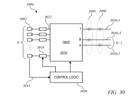
[0056] FIG. 30 shows an example of a switchable pairwise coupler circuit with
one
rasterized group of output paths according to some embodiments.
[0057] FIG. 31 shows a simplified schematic view of a Bell state generator
circuit
according to some embodiments.
DETAILED DESCRIPTION
[0058] Disclosed herein are examples (also referred to as "embodiments") of
circuits and
methods that implement multiplexing for photons propagating in waveguides. An
input
photon received on a selected one of a set of input waveguides can be
selectably routed to
one of a set of output waveguides. One or more of the output waveguides can be
always
selected while one or more other output waveguides can be selected on a
rotating or cyclic
basis, in a fixed order, and the input waveguide can be selected based at
least in part on which
one(s) of a set of input waveguides is (are) currently propagating a photon.
[0059] Circuits and methods of the kind described herein can be used in a
variety of
applications where spatial multiplexing is desired. To facilitate
understanding of the
disclosure, an overview of relevant concepts and terminology is provided in
Section 1.
Section 2 introduces spatial multiplexing techniques for photons in
waveguides. Sections 3
and 4 describe "raster" multiplexing techniques according to various
embodiments. Section 5
describes examples of generalized Mach Zehnder interferometer ("GMZI")
circuits that can
implement multiplexer circuits, including raster multiplexers. Section 6
describes examples
of circuits and methods using raster multiplexing techniques to produce Bell
states of
temporally encoded qubits. Although embodiments are described with specific
detail to
7
CA 03233277 2024-03-25
WO 2023/055829 PCT/US2022/045080
facilitate understanding, those skilled in the art with access to this
disclosure will appreciate
that the claimed invention can be practiced without these details.
1. Overview of Quantum Computing
[0060] Quantum computing relies on the dynamics of quantum objects, e.g.,
photons,
electrons, atoms, ions, molecules, nanostructures, and the like, which follow
the rules of
quantum theory. In quantum theory, the quantum state of a quantum object is
described by a
set of physical properties, the complete set of which is referred to as a
mode. In some
embodiments, a mode is defined by specifying the value (or distribution of
values) of one or
more properties of the quantum object. For example, in the case where the
quantum object is
a photon, modes can be defined by the frequency of the photon, the position in
space of the
photon (e.g., which waveguide or superposition of waveguides the photon is
propagating
within), the associated direction of propagation (e.g., the k-vector for a
photon in free space),
the polarization state of the photon (e.g., the direction (horizontal or
vertical) of the photon's
electric and/or magnetic fields), a time window in which the photon is
propagating, the
orbital angular momentum state of the photon, and the like.
[0061] For the case of photons propagating in a waveguide, it is convenient to
express the
state of the photon as one of a set of discrete spatio-temporal modes. For
example, the spatial
mode k of the photon is determined according to which one of a finite set of
discrete
waveguides the photon is propagating in, and the temporal mode tj is
determined by which
one of a set of discrete time periods (referred to herein as "bins") the
photon is present in. In
some photonic implementations, the degree of temporal discretization can be
provided by a
pulsed laser which is responsible for generating the photons. As used herein,
terms such as
"simultaneous" or "concurrent" refer to events occurring within the same time
bin, and terms
such as "synchronous" (or "synchronized") refer to events separated by a
predictable,
constant number of time bins, which can but need not be zero. The term "path"
is used herein
to refer to a set of one or more waveguides representing spatial modes, and
depending on
how the photons are being used, a path may include one or more waveguides. In
examples
below, spatial modes will be used primarily to avoid complication of the
description.
However, one of ordinary skill will appreciate that the systems and methods
can apply to any
.. type of mode, e.g., temporal modes, polarization modes, and any other mode
or set of modes
that serves to specify the quantum state. Further, in the description that
follows,
embodiments will be described that employ photonic waveguides to define the
spatial modes
of the photon. However, persons of ordinary skill in the art with access to
this disclosure will
8
CA 03233277 2024-03-25
WO 2023/055829 PCT/US2022/045080
appreciate that other types of mode, e.g., temporal modes, energy states, and
the like, can be
used without departing from the scope of the present disclosure. In addition,
persons of
ordinary skill in the art will be able to implement examples using other types
of quantum
systems, including but not limited to other types of photonic systems.
[0062] For quantum systems of multiple indistinguishable particles, rather
than describing
the quantum state of each particle in the system, it is useful to describe the
quantum state of
the entire many-body system using the formalism of Fock states (sometimes
referred to as the
occupation number representation). In the Fock state description, the many-
body quantum
state is specified by how many particles there are in each mode of the system.
For example, a
multi-mode, two particle Fock state 11001)1,2,3,4 specifies a two-particle
quantum state with
one particle in mode 1, zero particles in mode 2, zero particles in mode 3,
and one particle in
mode 4. Again, as introduced above, a mode can be any property of the quantum
object. For
the case of a photon, any two modes of the electromagnetic field can be used,
e.g., one may
design the system to use modes that are related to a degree of freedom that
can be
manipulated passively with linear optics. For example, polarization, spatial
degree of
freedom, or angular momentum could be used. The four-mode system represented
by the two
particle Fock state 11001)1,2,3,4 can be physically implemented as four
distinct waveguides
with two of the four waveguides having one photon travelling within them.
Other examples
of a state of such a many-body quantum system include the four-particle Fock
state
11111)1,2,3,4 that represents each mode occupied by one particle and the four-
particle Fock
state 12200)1,2,3,4 that represents modes 1 and 2 respectively occupied by two
particles and
modes 3 and 4 occupied by zero particles. For modes having zero particles
present, the term
"vacuum mode" is used. For example, for the four-particle Fock state
12200)1,2,3,4 modes 3
and 4 are referred to herein as "vacuum modes." Fock states having a single
occupied mode
can be represented in shorthand using a subscript to identify the occupied
mode. For
example, 10010)1,2,3,4 is equivalent to 113).
1.1.Qubits
[0063] As used herein, a "qubit" (or quantum bit) is a quantum system with an
associated
quantum state that can be used to encode information. A quantum state can be
used to
encode one bit of information if the quantum state space can be modeled as a
(complex) two-
dimensional vector space, with one dimension in the vector space being mapped
to logical
value 0 and the other to logical value 1. In contrast to classical bits, a
qubit can have a state
9
CA 03233277 2024-03-25
WO 2023/055829 PCT/US2022/045080
that is a superposition of logical values 0 and 1. More generally, a "qudit"
can be any
quantum system having a quantum state space that can be modeled as a (complex)
n-
dimensional vector space (for any integer n), which can be used to encode n
bits of
information. For the sake of clarity of description, the term "qubit" is used
herein, although
in some embodiments the system can also employ quantum information carriers
that encode
information in a manner that is not necessarily associated with a binary bit,
such as a qudit.
Qubits (or qudits) can be implemented in a variety of quantum systems.
Examples of qubits
include: polarization states of photons; presence of photons in waveguides; or
energy states
of molecules, atoms, ions, nuclei, or photons. Other examples include other
engineered
quantum systems such as flux qubits, phase qubits, or charge qubits (e.g.,
formed from a
superconducting Josephson junction); topological qubits (e.g., Majorana
fermions); or spin
qubits formed from vacancy centers (e.g., nitrogen vacancies in diamond).
[0064] A qubit can be "dual-rail encoded" such that the logical value of the
qubit is
encoded by occupation of one of two modes of the quantum system. For example,
the logical
0 and 1 values can be encoded as follows:
10)L = 110)1,2 (1)
11)L = 101)1,2 (2)
where the subscript "L" indicates that the ket represents a logical state
(e.g., a qubit value)
and, as before, the notation lij)1,2 on the right-hand side of the equations
above indicates that
there are i particles in a first mode and j particles in a second mode,
respectively (e.g., where i
and j are integers). In this notation, a two-qubit system having a logical
state 10)11)L
(representing a state of two qubits, the first qubit being in a '0' logical
state and the second
qubit being in a '1' logical state) may be represented using occupancy across
four modes by
11001)1,2,3,4 (e.g., in a photonic system, one photon in a first waveguide,
zero photons in a
second waveguide, zero photons in a third waveguide, and one photon in a
fourth
waveguide). In some instances throughout this disclosure, the various
subscripts are omitted
to avoid unnecessary mathematical clutter.
1.2.Entangled States
[0065] Many of the advantages of quantum computing relative to "classical"
computing
(e.g., conventional digital computers using binary logic) stem from the
ability to create
entangled states of multi-qubit systems. In mathematical terms, a state lip)
of n quantum
CA 03233277 2024-03-25
WO 2023/055829 PCT/US2022/045080
objects is a separable state if 10) = POO ¨010J and an entangled state is a
state that is
not separable. One example is a Bell state, which, loosely speaking, is a type
of maximally
entangled state for a two-qubit system, and qubits in a Bell state may be
referred to as a Bell
pair. For example, for qubits encoded by single photons in pairs of modes (a
dual-rail
encoding), examples of Bell states include:
+ 11)L11)L 110)110) + 101)101)
I>¨ _______________________________________________________________________
(3)
A/2 A/2
10)L10)L ¨ 11)L11)L 110)110) ¨ 101)101)
1(1)- = ___________________________________________________________________
(4)
A/2 A/2
10)L11)L + 110)101) + 101)110)
I>¨ _______________________________________________________________________
(5)
A/2 A/2
10)L11)L ¨ 11)L10)L 110)101) ¨ 101)110)
I>¨ _______________________________________________________________________
(6)
A/2 A/2
[0066] More generally, an n-qubit Greenberger-Horne-Zeilinger (GHZ) state (or
"n-GHZ
state") is an entangled quantum state of n qubits. For a given orthonormal
logical basis, an n-
GHZ state is a quantum superposition of all qubits being in a first basis
state superposed with
all qubits being in a second basis state:
10) NI +
1GHZ) = (7)
A/2
where the kets above refer to the logical basis. For example, for qubits
encoded by single
photons in pairs of modes (a dual-rail encoding), a 3-GHZ state can be
written:
10)L10)L10)L ¨ 11)L11)L11)L 110110110) + 101)101)101)
1GHZ) = _________________________________________________ (8)
A/2 A/2
where the kets above refer to photon occupation number in six respective modes
(with mode
subscripts omitted).
1.3.Physical Implementations
[0067] Qubits (and operations on qubits) can be implemented using a variety of
physical
systems. In some examples described herein, qubits are provided in an
integrated photonic
system employing waveguides, beam splitters, photonic switches, and single
photon
detectors, and the modes that can be occupied by photons are spatiotemporal
modes that
correspond to presence of a photon in a waveguide. Modes can be coupled using
mode
11
CA 03233277 2024-03-25
WO 2023/055829 PCT/US2022/045080
couplers, e.g., optical beam splitters, to implement transformation
operations, and
measurement operations can be implemented by coupling single-photon detectors
to specific
waveguides. One of ordinary skill in the art with access to this disclosure
will appreciate that
modes defined by any appropriate set of degrees of freedom, e.g., polarization
modes,
temporal modes, and the like, can be used without departing from the scope of
the present
disclosure. For instance, for modes that only differ in polarization (e.g.,
horizontal (H) and
vertical (V)), a mode coupler can be any optical element that coherently
rotates polarization,
e.g., a birefringent material such as a waveplate. For other systems such as
ion trap systems
or neutral atom systems, a mode coupler can be any physical mechanism that can
couple two
modes, e.g., a pulsed electromagnetic field that is tuned to couple two
internal states of the
atom/ion.
[0068] In some embodiments of a photonic quantum computing system using dual-
rail
encoding, a qubit can be implemented using a pair of waveguides. FIG. 1 shows
two
representations (100, 100') of a portion of a pair of waveguides 102, 104 that
can be used to
provide a dual-rail-encoded photonic qubit. At 100, a photon 106 is in
waveguide 102 and no
photon is in waveguide 104 (also referred to as a vacuum mode); in some
embodiments, this
corresponds to the I 0)L state of a photonic qubit. At 100', a photon 108 is
in waveguide 104,
and no photon is in waveguide 102; in some embodiments this corresponds to the
I1)L state
of the photonic qubit. To prepare a photonic qubit in a known logical state, a
photon source
(not shown) can be coupled to one end of one of the waveguides. The photon
source can be
operated to emit a single photon into the waveguide to which it is coupled,
thereby preparing
a photonic qubit in a known state. Photons travel through the waveguides, and
by
periodically operating the photon source, a quantum system having qubits whose
logical
states map to different temporal modes of the photonic system can be created
in the same pair
of waveguides. In addition, by providing multiple pairs of waveguides, a
quantum system
having qubits whose logical states correspond to different spatiotemporal
modes can be
created. It should be understood that the waveguides in such a system need not
have any
particular spatial relationship to each other. For instance, they can be but
need not be
arranged in parallel. In the context of optical circuits operating on qubits,
a "path" may refer
to a set of (one or more) waveguides that provides a set of spatial modes for
one qubit. In a
dual-rail encoding, a path includes a pair of waveguides. Since each waveguide
in a dual-rail
encoding corresponds to a (spatial) mode, the term "mode" is sometimes used
interchangeably with "waveguide" in descriptions of circuits for dual-rail
encoded qubits.
12
CA 03233277 2024-03-25
WO 2023/055829 PCT/US2022/045080
Other encodings may use a different number of waveguides. For instance, a
polarization
encoding may use a single waveguide for each path.
[0069] Occupied modes can be created by using a photon source to generate a
photon that
then propagates in the desired waveguide. A photon source can be, for
instance, a resonator-
.. based source that emits photon pairs, also referred to as a heralded single
photon source. In
one example of such a source, the source is driven by a pump, e.g., a light
pulse, that is
coupled into a system of optical resonators that, through a nonlinear optical
process (e.g.,
spontaneous four wave mixing (SFWM), spontaneous parametric down-conversion
(SPDC),
second harmonic generation, or the like), can generate a pair of photons. Many
different
types of photon sources can be employed. Examples of photon pair sources can
include a
microring-based spontaneous four wave mixing (SPFW) heralded photon source
(HPS).
However, the precise type of photon source used is not critical and any type
of nonlinear
source, employing any process, such as SPFW, SPDC, or any other process can be
used.
Other classes of sources that do not necessarily require a nonlinear material
can also be
.. employed, such as those that employ atomic and/or artificial atomic
systems, e.g., quantum
dot sources, color centers in crystals, and the like. In some cases, sources
may or may not be
coupled to photonic cavities, e.g., as can be the case for artificial atomic
systems such as
quantum dots coupled to cavities. Other types of photon sources also exist for
SFWM and
SPDC, such as optomechanical systems and the like. For purposes of the present
disclosure,
the precise type of photon source used is not critical and any type of
heralded single photon
source, employing any process, such as SPFW, SPDC, or any other process, can
be used.
[0070] In such cases, operation of the photon source may be non-deterministic
(also
sometimes referred to as "stochastic") such that a given pump pulse may or may
not produce
a photon pair. In some embodiments, when a heralded single photon source
generates a pair
of photons, one photon of the pair can be propagated into a "signaling" (or
"propagation")
waveguide of an optical circuit, and the other photon (sometimes referred to
as a "heralding
photon") can be propagated into a different waveguide, which can be coupled to
a single-
photon detector. The single-photon detector can generate a signal (e.g., a
digital logic signal)
indicating when a photon has been detected by the detector. Any type of
photodetector that
has sensitivity to single photons can be used. In some embodiments, detection
of a photon in
a particular heralding waveguide indicates presence of a photon in a
corresponding signaling
waveguide. Accordingly, it can be known when and where a photon is generated.
13
CA 03233277 2024-03-25
WO 2023/055829 PCT/US2022/045080
[0071] In some embodiments, coherent spatial and/or temporal multiplexing of
several
non-deterministic sources (referred to herein as "active" multiplexing) can be
used to allow
the probability of having one mode become occupied during a given cycle to
approach 1.
One of ordinary skill will appreciate that many different active multiplexing
architectures that
.. incorporate spatial and/or temporal multiplexing are possible. For
instance, active
multiplexing schemes that employ log-tree, generalized Mach-Zehnder
interferometers,
multimode interferometers, chained sources, chained sources with dump-the-pump
schemes,
asymmetric multi-crystal single photon sources, or any other type of active
multiplexing
architecture can be used. In some embodiments, the photon source can employ an
active
multiplexing scheme with quantum feedback control and the like. In some
embodiments, use
of multirail encoding allows the probability of a band having one mode become
occupied
during a given pulse cycle to approach 1 without active multiplexing. Specific
examples of
multiplexing operations that can be applied to non-deterministic photon
sources are described
below.
[0072] Measurement operations can be implemented by coupling a waveguide to a
single-
photon detector that generates a classical signal (e.g., a digital logic
signal) indicating that a
photon has been detected by the detector. Any type of photodetector that has
sensitivity to
single photons can be used. In some embodiments, detection of a photon (e.g.,
at the output
end of a waveguide) indicates an occupied mode while absence of a detected
photon can
indicate an unoccupied mode.
[0073] Some embodiments described below relate to physical implementations of
unitary
transform operations that couple modes of a quantum system, which can be
understood as
transforming the quantum state of the system. For instance, if the initial
state of the quantum
system (prior to mode coupling) is one in which one mode is occupied with
probability 1 and
another mode is unoccupied with probability 1 (e.g., a state 110) in the Fock
notation
introduced above), mode coupling can result in a state in which both modes
have a nonzero
probability of being occupied, e.g., a state a1110) + a2101), where Ia1I2 +
1a212 = 1. In
some embodiments, operations of this kind can be implemented by using beam
splitters to
couple modes together and variable phase shifters to apply phase shifts to one
or more modes.
.. The amplitudes al and az depend on the reflectivity (or transmissivity) of
the beam splitters
and on any phase shifts that are introduced.
14
CA 03233277 2024-03-25
WO 2023/055829 PCT/US2022/045080
[0074] FIG. 2A shows a schematic diagram 210 (also referred to as a circuit
diagram or
circuit notation) for coupling of two modes. The modes are drawn as horizontal
lines 212,
214, and the mode coupler 216 is indicated by a vertical line that is
terminated with nodes
(solid dots) to identify the modes being coupled. In the more specific
language of linear
quantum optics, the mode coupler 216 shown in FIG. 2A represents a 50/50 beam
splitter that
implements a transfer matrix:
T = ¨1 (1- i)
i (9)
where T defines the linear map for the photon creation operators on two modes.
(In certain
contexts, transfer matrix T can be understood as implementing a first-order
imaginary
Hadamard transform.) By convention the first column of the transfer matrix
corresponds to
creation operators on the top mode (referred to herein as mode 1, labeled as
horizontal line
212), and the second column corresponds to creation operators on the second
mode (referred
to herein as mode 2, labeled as horizontal line 214), and so on if the system
includes more
than two modes. More explicitly, the mapping can be written as:
(4) ,3 1 ( 1 _i) (al)
A/7 1 )t ) output (10)
input
where subscripts on the creation operators indicate the mode that is operated
on, the
subscripts input and output identify the form of the creation operators before
and after the
beam splitter, respectively and where:
ai Int, ni) = Int ¨ 1,n1)
ai ni) Int, ni ¨1) (11)
at n, n1) = _jrzi + 1n, n1 + 1)
I
For example, the application of the mode coupler shown in FIG. 2A leads to the
following
mappings:
1
at
1 input " ¨ (a1toutput ¨ i
1/7 output) (12)
CA 03233277 2024-03-25
WO 2023/055829 PCT/US2022/045080
1
ain 1, ¨ i a it +a ,t
put
1/7 output output)
Thus, the action of the mode coupler described by Eq. (9) is to take the input
states
110,101), and Ill) to
110>¨ il01)
110)
A/2
¨00) + 101)
101)
(13)
A/2
111) ¨2 (120) +102))
[0075] FIG. 2B shows a physical implementation of a mode coupling that
implements the
transfer matrix T of Eq. (9) for two photonic modes in accordance with some
embodiments.
In this example, the mode coupling is implemented using a waveguide beam
splitter 200, also
sometimes referred to as a directional coupler or mode coupler. Waveguide beam
splitter 200
can be realized by bringing two waveguides 202, 204 into close enough
proximity that the
evanescent field of one waveguide can couple into the other. By adjusting the
separation d
between waveguides 202, 204 and/or the length / of the coupling region,
different couplings
between modes can be obtained. In this manner, a waveguide beam splitter 200
can be
configured to have a desired transmissivity. For example, the beam splitter
can be engineered
to have a transmissivity equal to 0.5 (i.e., a 50/50 beam splitter for
implementing the specific
form of the transfer matrix T introduced above). If other transfer matrices
are desired, the
reflectivity (or the transmissivity) can be engineered to be greater than 0.6,
greater than 0.7,
greater than 0.8, or greater than 0.9 without departing from the scope of the
present
disclosure.
[0076] In addition to mode coupling, some unitary transforms may involve phase
shifts
applied to one or more modes. In some photonic implementations, variable phase-
shifters
can be implemented in integrated circuits, providing control over the relative
phases of the
state of a photon spread over multiple modes. Examples of transfer matrices
that define such
a phase shifts are given by (for applying a +i and ¨i phase shift to the
second mode,
respectively):
s = (1 0)
(14)
)
16
CA 03233277 2024-03-25
WO 2023/055829 PCT/US2022/045080
= t(1 0
0 -i)
For silica-on-silicon materials some embodiments implement variable phase-
shifters using
thermo-optical switches. The thermo-optical switches use resistive elements
fabricated on
the surface of the chip, that via the thermo-optical effect can provide a
change of the
refractive index n by raising the temperature of the waveguide by an amount of
the order of
10-5K. One of skill in the art with access to the present disclosure will
understand that any
effect that changes the refractive index of a portion of the waveguide can be
used to generate
a variable, electrically tunable, phase shift. For example, some embodiments
use beam
splitters based on any material that supports an electro-optic effect, so-
called x2 and x3
materials such as lithium niobite, BBO, KTP, and the like and even doped
semiconductors
such as silicon, germanium, and the like.
[0077] Beam-splitters with variable transmissivity and arbitrary phase
relationships
between output modes can also be achieved by combining directional couplers
and variable
phase-shifters in a Mach-Zehnder Interferometer (MU) configuration 300, e.g.,
as shown in
FIG. 3A. Complete control over the relative phase and amplitude of the two
modes 302a,
302b in dual rail encoding can be achieved by varying the phases imparted by
phase shifters
306a, 306b, and 306c and the length and proximity of coupling regions 304a and
304b. FIG.
3B shows a slightly simpler example of a MZI 310 that allows for a variable
transmissivity
between modes 302a, 302b by varying the phase imparted by the phase shifter
306. FIGs. 3A
and 3B are examples of how one could implement a mode coupler in a physical
device, but
any type of mode coupler/beam splitter can be used without departing from the
scope of the
present disclosure.
[0078] In some embodiments, beam splitters and phase shifters can be employed
in
combination to implement a variety of transfer matrices. For example, FIG. 4A
shows, in a
schematic form similar to that of FIG. 2A, a mode coupler 400 implementing the
following
transfer matrix:
Tr = - 11 ( 1
(15)
q
Thus, mode coupler 400 applies the following mappings:
17
CA 03233277 2024-03-25
WO 2023/055829 PCT/US2022/045080
I10>+ 101)
110)
A/2
110>- 101)
101)
(16)
A/2
1
111) ¨2 (120) +102)).
The transfer matrix Tr of Eq. (15) is related to the transfer matrix T of Eq.
(9) by a phase shift
on the second mode. This is schematically illustrated in FIG. 4A by the closed
node 407
where mode coupler 416 couples to the first mode (line 212) and open node 408
where mode
coupler 416 couples to the second mode (line 214). More specifically, Tr =
sTs, and, as
shown at the right-hand side of FIG. 4A, mode coupler 416 can be implemented
using mode
coupler 216 (as described above), with a preceding and following phase shift
(denoted by
open squares 418a, 418b). Thus, the transfer matrix Tr can be implemented by
the physical
beam splitter shown in FIG. 4B, where the open triangles represent +i phase
shifters.
[0079] Similarly, networks of mode couplers and phase shifters can be used to
implement
couplings among more than two modes. For example, FIG. 5 shows a four-mode
coupling
scheme that implements a "spreader," or "mode-information erasure,"
transformation on four
modes, i.e., it takes a photon in any one of the input modes and delocalizes
the photon
amongst each of the four output modes such that the photon has equal
probability of being
detected in any one of the four output modes. (The well-known Hadamard
transformation is
one example of a spreader transformation that can be applied to a set of 2q
modes for integer
q.) As in FIG. 2A, the horizontal lines 512-515 correspond to modes, and the
mode coupling
is indicated by a vertical line 516 with nodes (dots) to identify the modes
being coupled. In
this case, four modes are coupled. Circuit notation 502 is an equivalent
representation to
circuit diagram 504, which is a network of first-order mode couplings. More
generally,
where a higher-order mode coupling can be implemented as a network of first-
order mode
couplings, a circuit notation similar to notation 502 (with an appropriate
number of modes)
may be used.
[0080] FIG. 6 illustrates an example optical device 600 that can implement the
four-mode
mode-spreading transform shown schematically in FIG. 5 in accordance with some
embodiments. Optical device 600 includes a first set of optical waveguides
601, 603 formed
in a first layer of material (represented by solid lines in FIG. 6) and a
second set of optical
18
CA 03233277 2024-03-25
WO 2023/055829 PCT/US2022/045080
waveguides 605, 607 formed in a second layer of material that is distinct and
separate from
the first layer of material (represented by dashed lines in FIG. 6). The
second layer of
material and the first layer of material are located at different heights on a
substrate. One of
ordinary skill will appreciate that an interferometer such as that shown in
FIG. 6 could be
.. implemented in a single layer if appropriate low loss waveguide crossing
were employed.
[0081] At least one optical waveguide 601, 603 of the first set of optical
waveguides is
coupled with an optical waveguide 605, 607 of the second set of optical
waveguides with any
type of suitable optical coupler, e.g., the directional couplers described
herein (e.g., the
optical couplers shown in FIGs. 2B, 3A, 3B). For example, the optical device
shown in FIG.
.. 6 includes four optical couplers 618, 620, 622, and 624. Each optical
coupler can have a
coupling region in which two waveguides propagate in parallel. Although the
two
waveguides are illustrated in FIG. 6 as being offset from each other in the
coupling region,
the two waveguides may be positioned directly above and below each other in
the coupling
region without offset. In some embodiments, one or more of the optical
couplers 618, 620,
622, and 624 are configured to have a coupling efficiency of approximately 50%
between the
two waveguides (e.g., a coupling efficiency between 49% and 51%, a coupling
efficiency
between 49.9% and 50.1%, a coupling efficiency between 49.99% and 50.01%, and
a
coupling efficiency of 50%, etc.). For example, the length of the two
waveguides, the
refractive indices of the two waveguides, the widths and heights of the two
waveguides, the
refractive index of the material located between two waveguides, and the
distance between
the two waveguides are selected to provide the coupling efficiency of 50%
between the two
waveguides. This allows the optical coupler to operate like a 50/50 beam
splitter.
[0082] In addition, the optical device shown in FIG. 6 can include two inter-
layer optical
couplers 614 and 616. Optical coupler 614 allows transfer of light propagating
in a
.. waveguide on the first layer of material to a waveguide on the second layer
of material, and
optical coupler 616 allows transfer of light propagating in a waveguide on the
second layer of
material to a waveguide on the first layer of material. The optical couplers
614 and 616 allow
optical waveguides located in at least two different layers to be used in a
multi-channel
optical coupler, which, in turn, enables a compact multi-channel optical
coupler.
.. [0083] Furthermore, the optical device shown in FIG. 6 includes a non-
coupling waveguide
crossing region 626. In some implementations, the two waveguides (603 and 605
in this
example) cross each other without having a parallel coupling region present at
the crossing in
19
CA 03233277 2024-03-25
WO 2023/055829 PCT/US2022/045080
the non-coupling waveguide crossing region 626 (e.g., the waveguides can be
two straight
waveguides that cross each other at a nearly 90-degree angle).
[0084] Those skilled in the art will understand that the foregoing examples
are illustrative
and that photonic circuits using beam splitters and/or phase shifters can be
used to implement
many different transfer matrices, including transfer matrices for real and
imaginary
Hadamard transforms of any order, discrete Fourier transforms, and the like.
One class of
photonic circuits, referred to herein as "spreader" or "mode-information
erasure (MIE)"
circuits, has the property that if the input is a single photon localized in
one input mode, the
circuit delocalizes the photon amongst each of a number of output modes such
that the
photon has equal probability of being detected in any one of the output modes.
Examples of
spreader or MIE circuits include circuits implementing Hadamard transfer
matrices. (It is to
be understood that spreader or MIE circuits may receive an input that is not a
single photon
localized in one input mode, and the behavior of the circuit in such cases
depends on the
particular transfer matrix implemented.) In other instances, photonic circuits
can implement
other transfer matrices, including transfer matrices that, for a single photon
in one input
mode, provide unequal probability of detecting the photon in different output
modes.
[0085] In some embodiments, entangled states of multiple photonic qubits can
be created
by coupling (spatial) modes of two (or more) qubits and performing
measurements on other
modes. By way of example, FIG. 7 shows a circuit diagram for a Bell state
generator 700
that can be used in some dual-rail-encoded photonic embodiments. In this
example,
waveguides (or modes) 732-1 through 732-4 are initially each occupied by a
photon
(indicated by a wavy line); waveguides (or modes) 732-5 through 732-8 are
initially vacuum
(unoccupied) modes. (Those skilled in the art will appreciate that other
combinations of
occupied and unoccupied modes can be used.)
[0086] A first-order mode coupling (e.g., implementing transfer matrix T of
Eq. (9)) is
performed on pairs of occupied and unoccupied modes as shown by mode couplers
731-1-
731-4, with each mode coupler 731 having one input waveguide receiving a
photon and one
input waveguide receiving vacuum. Mode couplers 731 can be, e.g., 50/50 beam
splitters so
that, for example, a photon entering on waveguide 732-1 (or a photon entering
on waveguide
732-5) has a 50% probability of emerging on either output of mode coupler 731-
1. In the
following description, mode couplers 731 may also be referred to as
"directional couplers."
Thereafter, a mode-information erasure coupling (e.g., implementing a four-
mode mode
CA 03233277 2024-03-25
WO 2023/055829 PCT/US2022/045080
spreading transform as shown in FIG. 5 or a second-order Hadamard transfer
matrix) is
performed on one output mode of each directional coupler 731 (in this example,
waveguides
733-5 through 733-8 provide inputs to the mode-information erasure coupling),
as shown by
mode coupler 737. In the following description, mode coupler 737 may also be
referred to as
a "mode coupler network" or "Hadamard network." Waveguides 733-5 through 733-8
act as
"heralding" modes that are measured and used to determine whether a Bell state
was
successfully generated on the four output waveguides 733-1 through 733-4. For
instance,
detectors 738-1 through 738-4 can be coupled to the waveguides 733-5 through
733-8 after
second-order mode coupler 737. Each detector 738-1 through 738-4 can output a
classical
data signal (e.g., a voltage level on a conductor) indicating whether it
detected a photon (or
the number of photons detected). These outputs can be coupled to classical
decision logic
circuit 740, which determines whether a Bell state is present on the other
four waveguides
733-1 through 733-4. For example, decision logic circuit 740 can be configured
such that a
Bell state is confirmed (also referred to as "success" of the Bell state
generator) if and only if
a single photon was detected by each of exactly two of detectors 738-1 through
738-4. In
some embodiments, output modes (or waveguides) 733-1 through 733-4 can be
mapped to
the logical states of two qubits (Qubit 1 and Qubit 2), as indicated in FIG.
7. Specifically, in
this example, the logical state of Qubit 1 is based on occupancy of modes 733-
1 and 733-2,
and the logical state of Qubit 2 is based on occupancy of modes 733-3 and 733-
4. It should
be noted that generation of a Bell state by Bell state generator 700 is a non-
deterministic (or
stochastic) process; that is, inputting four photons as shown does not
guarantee that a Bell
state will be created on modes 733-1 through 733-4. In one implementation, the
probability
of success is 4/32; in another implementation, the success probability is
3/16. It should also
be noted that there are six detection patterns with one photon in each of two
of detectors 738,
.. and that Bell state generator 700 can be expected to produce a Bell state
in all six possible
arrangements of the four output modes. For a given choice of assignment of
modes to dual-
rail qubits (e.g., as shown in FIG. 7), Bell state generator 700 can produce
any of the four
two-qubit Bell states defined in Eqs. (3)-(6) above, as well as a "non-qubit"
maximally
entangled state. Different detection patterns at detectors 738 can correspond
to different
types of Bell states being produced. In some embodiments, based on the
particular detection
pattern at detectors 738, mode swaps can be selectably applied to modes 733 in
order to cast
the Bell state into a particular type (e.g., a particular one of the four two-
qubit Bell states
defined above). In some embodiments, the mode swap can be subsumed into
subsequent
21
CA 03233277 2024-03-25
WO 2023/055829 PCT/US2022/045080
operations without the need for active optical switches to implement
selectable mode
swapping at the output of Bell state generator 700.
[0087] In some embodiments, it is desirable to form cluster states of multiple
entangled
qubits (typically 3 or more qubits, although the Bell state can be understood
as a cluster state
of two qubits). One technique for forming larger entangled systems is through
the use of an
entangling measurement, which is a projective measurement that can be employed
to create
entanglement between systems of qubits. As used herein, "fusion" (or "a fusion
operation" or
"fusing") refers to a two-qubit entangling measurement. A "fusion gate" is a
structure that
receives two input qubits, each of which is typically part of an entangled
system. The fusion
gate performs a projective measurement operation on the input qubits that
produces either
one ("type I fusion") or zero ("type II fusion") output qubits in a manner
such that the initial
two entangled systems are fused into a single entangled system. Fusion gates
are specific
examples of a general class of two-qubit entangling measurements and are
particularly suited
for photonic architectures. Examples of type I and type II fusion gates will
now be described.
[0088] FIG. 8A shows a circuit diagram illustrating a type I fusion gate 800
in accordance
with some embodiments. The diagram shown in FIG. 8A is schematic with each
horizontal
line representing a mode of a quantum system, e.g., a photon. In a dual-rail
encoding, each
pair of modes represents a qubit. In a photonic implementation of the gate the
modes in
diagrams such as that shown in FIG. 8A can be physically realized using single
photons in
photonic waveguides. Most generally, a type I fusion gate like that shown in
FIG. 8A takes
qubit A (physically realized, e.g., by photon modes 843 and 845) and qubit B
(physically
realized, e.g., by photon modes 847 and 849) as input and outputs a single
"fused" qubit that
inherits the entanglement with other qubits that were previously entangled
with either (or
both) of input qubit A or input qubit B.
[0089] For example, FIG. 8B shows the result of type-I fusing of two qubits A
and B that
are each, respectively, a qubit located at the end (i.e., a leaf) of some
longer entangled cluster
state (only a portion of which is shown). The qubit 857 that remains after the
fusion operation
inherits the entangling bonds from the original qubits A and B thereby
creating a larger linear
cluster state. FIG. 8B also shows the result of type-I fusing of two qubits A
and B that are
each, respectively, an internal qubit that belongs to some longer entangled
cluster of qubits
(only a portion of which is shown). As before, the qubit 859 that remains
after fusion inherits
the entangling bonds from the original qubits A and B thereby creating a fused
cluster state.
22
CA 03233277 2024-03-25
WO 2023/055829 PCT/US2022/045080
In this case, the qubit that remains after the fusion operation is entangled
with the larger
cluster by way of four other nearest neighbor qubits as shown.
[0090] Returning to the schematic illustration of type I fusion gate 800 shown
in FIG. 8A,
qubit A is dual-rail encoded by modes 843 and 845, and qubit B is dual-rail
encoded by
modes 847 and 849. For example, in the case of path-encoded photonic qubits,
the logical
zero state of qubit A (denoted I 0)A) occurs when mode 843 is a photonic
waveguide that
includes a single photon and mode 845 is a photonic waveguide that includes
zero photons
(and likewise for qubit B). Thus, type I fusion gate 800 can take as input two
dual-rail-
encoded photon qubits thereby resulting in a total of four input modes (e.g.,
modes 843, 845,
847, and 849). To accomplish the fusion operation, a mode coupler (e.g., 50/50
beam
splitter) 853 is applied between a mode of each of the input qubits, e.g.,
between mode 843
and mode 849 before performing a detection operation on both modes using
photon detectors
855 (which includes two distinct photon detectors coupled to modes 843 and 849
respectively). In addition, to ensure that the output modes are adjacently
positioned, a mode
swap operation 851 can be applied that swaps the position of the second mode
of qubit A
(mode 845) with the position the second mode of qubit B (mode 849). In some
embodiments,
mode swapping can be accomplished through a physical waveguide crossing as
described
above or by one or more photonic switches or by any other type of physical
mode swap.
[0091] FIG. 8A shows only an example arrangement for a type I fusion gate and
one of
ordinary skill will appreciate that the position of the mode coupler and the
presence of the
mode swap region 851 can be altered without departing from the scope of the
present
disclosure. For example, beam splitter 853 can be applied between modes 845
and 847.
Mode swaps are optional and are not necessary if qubits having non-adjacent
modes can be
dealt with, e.g., by tracking which modes belong to which qubits by storing
this information
in a classical memory.
[0092] Type I fusion gate 800 is a nondeterministic gate, i.e., the fusion
operation succeeds
with a certain probability less than 1, and in other cases the quantum state
that results is not a
larger cluster state that comprises the original cluster states fused together
to a larger cluster
state. More specifically, gate 800 "succeeds," with probability 50%, when only
one photon is
detected by detectors 855, and "fails" if zero or two photons are detected by
detectors 855.
When the gate succeeds, the two cluster states that qubits A and B were a part
of become
fused into a single larger cluster state with a fused qubit remaining as the
qubit that links the
23
CA 03233277 2024-03-25
WO 2023/055829 PCT/US2022/045080
two previously unlinked cluster states (see, e.g., FIG. 8B). However, when the
fusion gate
fails, it has the effect of removing both qubits from the original cluster
resource states without
generating a larger fused state.
[0093] FIG. 9A shows a circuit diagram illustrating a type II fusion gate 900
in accordance
with some embodiments. Like other diagrams herein, the diagram shown in FIG.
9A is
schematic with each horizontal line representing a mode of a quantum system,
e.g., a photon.
In a dual-rail encoding, each pair of modes represents a qubit. In a photonic
implementation
of the gate the modes in diagrams such as that shown in FIG. 9A can be
physically realized
using single photons in photonic waveguides. Most generally, a type II fusion
gate such as
gate 900 takes qubit A (physically realized, e.g., by photon modes 943 and
945) and qubit B
(physically realized, e.g., by photon modes 947 and 949) as input and outputs
a quantum state
that inherits the entanglement with other qubits that were previously
entangled with either (or
both) of input qubit A or input qubit B. (For type II fusion, if the input
quantum state had N
qubits, the output quantum state has N¨ 2 qubits. This is different from type
I fusion where
an input quantum state of N qubits leads to an output quantum state having N¨
1 qubits.)
[0094] For example, FIG. 9B shows the result of type-II fusing of two qubits A
and B that
are each, respectively, a qubit located at the end (i.e., a leaf) of some
longer entangled cluster
state (only a portion of which is shown). The resulting qubit system 971
inherits the
entangling bonds from qubits A and B thereby creating a larger linear cluster
state.
[0095] Returning to the schematic illustration of type II fusion gate 900
shown in FIG. 9A,
qubit A is dual-rail encoded by modes 943 and 945, and qubit B is dual-rail
encoded by
modes 947 and 949. For example, in the case of path encoded photonic qubits,
the logical
zero state of qubit A (denoted I 0)A) occurs when mode 943 is a photonic
waveguide that
includes a single photon and mode 945 is a photonic waveguide that includes
zero photons
(and likewise for qubit B). Thus, type II fusion gate 900 takes as input two
dual-rail-encoded
photon qubits thereby resulting in a total of four input modes (e.g., modes
943, 945, 947, and
949). To accomplish the fusion operation, a first mode coupler (e.g., 50/50
beam splitter) 953
is applied between a mode of each of the input qubits, e.g., between mode 943
and mode 949,
and a second mode coupler (e.g., 50/50 beam splitter) 955 is applied between
the other modes
of each of the input qubits, e.g., between modes 945 and 947. A detection
operation is
performed on all four modes using photon detectors 957(1)-957(4). In some
embodiments,
mode swap operations (not shown in FIG. 9A) can be performed to place modes in
adjacent
24
CA 03233277 2024-03-25
WO 2023/055829 PCT/US2022/045080
positions prior to mode coupling. In some embodiments, mode swapping can be
accomplished through a physical waveguide crossing as described above or by
one or more
photonic switches or by any other type of physical mode swap. Mode swaps are
optional and
are not necessary if qubits having non-adjacent modes can be dealt with, e.g.,
by tracking
which modes belong to which qubits by storing this information in a classical
memory.
[0096] FIG. 9A shows only an example arrangement for the type II fusion gate
and one of
ordinary skill will appreciate that the positions of the mode couplers and the
presence or
absence of mode swap regions can be altered without departing from the scope
of the present
disclosure.
[0097] The type II fusion gate shown in FIG. 9A is a nondeterministic gate,
i.e., the fusion
operation succeeds with a certain probability less than 1, and in other cases
the quantum state
that results is not a larger cluster state that comprises the original cluster
states fused together
to a larger cluster state. More specifically, the gate "succeeds" in the case
where one photon
is detected by one of detectors 957(1) and 957(4) and one photon is detected
by one of
detectors 957(2) and 957(3); in all other cases, the gate "fails." When the
gate succeeds, the
two cluster states that qubits A and B were a part of become fused into a
single larger cluster
state; unlike type-I fusion, no fused qubit remains (compare FIG. 8B and FIG.
9B). When the
fusion gate fails, it has the effect of removing both qubits from the original
cluster resource
states without generating a larger fused state.
[0098] FIG. 10 illustrates an example of a qubit entangling system 1001 in
accordance with
some embodiments. Such a system can be used to generate qubits (e.g., photons)
in an
entangled state (e.g., a GHZ state, Bell pair, and the like), in accordance
with some
embodiments.
[0099] In an illustrative photonic architecture, qubit entangling system 1001
can include a
photon source module 1005 that is optically connected to entangled state
generator 1000.
Both the photon source module 1005 and the entangled state generator 1000 may
be coupled
to a classical processing system 1003 such that the classical processing
system 1003 can
communicate and/or control (e.g., via the classical information channels 1030a-
b) the photon
source module 1005 and/or the entangled state generator 1000. Photon source
module 1005
may include a collection of single-photon sources that can provide output
photons to
entangled state generator 1000 by way of interconnecting waveguides 1032.
Entangled state
generator 1000 may receive the output photons and convert them to one or more
entangled
CA 03233277 2024-03-25
WO 2023/055829 PCT/US2022/045080
photonic states and then output these entangled photonic states into output
waveguides 1040.
In some embodiments, output waveguide 1040 can be coupled to some downstream
circuit
that may use the entangled states for performing a quantum computation. For
example, the
entangled states generated by the entangled state generator 1000 may be used
as resources for
a downstream quantum optical circuit (not shown).
[0100] In some embodiments, system 1001 may include classical channels 1030
(e.g.,
classical channels 1030-a through 1030-d) for interconnecting and providing
classical
information between components. It should be noted that classical channels
1030-a through
1030-d need not all be the same. For example, classical channel 1030-a through
1030-c may
comprise a bi-directional communication bus carrying one or more reference
signals, e.g.,
one or more clock signals, one or more control signals, or any other signal
that carries
classical information, e.g., heralding signals, photon detector readout
signals, and the like.
[0101] In some embodiments, qubit entangling system 1001 includes the
classical
computer system 1003 that communicates with and/or controls the photon source
module
1005 and/or the entangled state generator 1000. For example, in some
embodiments, classical
computer system 1003 can be used to configure one or more circuits, e.g.,
using system clock
that may be provided to photon sources 1005 and entangled state generator 1000
as well as
any downstream quantum photonic circuits used for performing quantum
computation. In
some embodiments, the quantum photonic circuits can include optical circuits,
electrical
circuits, or any other types of circuits. In some embodiments, classical
computer system 1003
includes memory 1004, one or more processor(s) 1002, a power supply, an
input/output (I/O)
subsystem, and a communication bus or interconnecting these components. The
processor(s)
1002 may execute modules, programs, and/or instructions stored in memory 1004
and
thereby perform processing operations.
[0102] In some embodiments, memory 1004 stores one or more programs (e.g.,
sets of
instructions) and/or data structures. For example, in some embodiments,
entangled state
generator 1000 can attempt to produce an entangled state over successive
stages, any one of
which may be successful in producing an entangled state. In some embodiments,
memory
1004 stores one or more programs for determining whether a respective stage
was successful
and configuring the entangled state generator 1000 accordingly (e.g., by
configuring
entangled state generator 1000 to switch the photons to an output if the stage
was successful,
or pass the photons to the next stage of the entangled state generator 1000 if
the stage was not
26
CA 03233277 2024-03-25
WO 2023/055829 PCT/US2022/045080
yet successful). To that end, in some embodiments, memory 1004 stores
detection patterns
(described below) from which the classical computing system 1003 may determine
whether a
stage was successful. In addition, memory 1004 can store settings that are
provided to the
various configurable components (e.g., switches) described herein that are
configured by,
e.g., setting one or more phase shifts for the component.
[0103] In some embodiments, some or all of the above-described functions may
be
implemented with hardware circuits on photon source module 1005 and/or
entangled state
generator 1000. For example, in some embodiments, photon source module 1005
includes
one or more controllers 1007-a (e.g., logic controllers) (e.g., which may
comprise field
programmable gate arrays (FPGAs), application specific integrated circuits
(ASICS), a
"system on a chip" that includes classical processors and memory, or the
like). In some
embodiments, controller 1007-a determines whether photon source module 1005
was
successful (e.g., for a given attempt on a given clock cycle, described below)
and outputs a
reference signal indicating whether photon source module 1005 was successful.
For example,
in some embodiments, controller 1007-a outputs a logical high value to
classical channel
1030-a and/or classical channel 1030-c when photon source module 1005 is
successful and
outputs a logical low value to classical channel 1030-a and/or classical
channel 1030-c when
photon source module 1005 is not successful. In some embodiments, the output
of control
1007-a may be used to configure hardware in controller 1007-b.
[0104] Similarly, in some embodiments, entangled state generator 1000 includes
one or
more controllers 1007-b (e.g., logical controllers) (e.g., which may comprise
field
programmable gate arrays (FPGAs), application specific integrated circuits
(ASICS), or the
like) that determine whether a respective stage of entangled state generator
1000 has
succeeded, perform the switching logic described above, and output a reference
signal to
.. classical channels 1030-b and/or 1030-d to inform other components as to
whether the
entangled state generator 400 has succeeded.
[0105] In some embodiments, a system clock signal can be provided to photon
source
module 1005 and entangled state generator 1000 via an external source (not
shown) or by
classical computing system 1003 generates via classical channels 1030-a and/or
1030-b. In
some embodiments, the system clock signal provided to photon source module
1005 triggers
photon source module 1005 to attempt to output one photon per waveguide. In
some
embodiments, the system clock signal provided to entangled state generator
1000 triggers, or
27
CA 03233277 2024-03-25
WO 2023/055829 PCT/US2022/045080
gates, sets of detectors in entangled state generator 1000 to attempt to
detect photons. For
example, in some embodiments, triggering a set of detectors in entangled state
generator
1000 to attempt to detect photons includes gating the set of detectors.
[0106] It should be noted that, in some embodiments, photon source module 1005
and
.. entangled state generator 1000 may have internal clocks. For example,
photon source module
1005 may have an internal clock generated and/or used by controller 1007-a and
entangled
state generator 1000 has an internal clock generated and/or used by controller
1007-b. In
some embodiments, the internal clock of photon source module 1005 and/or
entangled state
generator 1000 is synchronized to an external clock (e.g., the system clock
provided by
classical computer system 1003) (e.g., through a phase-locked loop). In some
embodiments,
any of the internal clocks may themselves be used as the system clock, e.g.,
an internal clock
of the photon source may be distributed to other components in the system and
used as the
master/system clock.
[0107] In some embodiments, photon source module 1005 includes a plurality of
probabilistic photon sources that may be spatially and/or temporally
multiplexed, i.e., a so-
called multiplexed single photon source. In one example of such a source, the
source is
driven by a pump, e.g., a light pulse, that is coupled into an optical
resonator that, through
some nonlinear process (e.g., spontaneous four wave mixing, second harmonic
generation,
and the like) may generate zero, one, or more photons. As used herein, the
term "attempt" is
used to refer to the act of driving a photon source with some sort of driving
signal, e.g., a
pump pulse, that may produce output photons non-deterministically (i.e., in
response to the
driving signal, the probability that the photon source will generate one or
more photons may
be less than 1). In some embodiments, a respective photon source may be most
likely to, on a
respective attempt, produce zero photons (e.g., there may be a 90% probability
of producing
zero photons per attempt to produce a single-photon). The second most likely
result for an
attempt may be production of a single-photon (e.g., there may be a 9%
probability of
producing a single-photon per attempt to produce a single-photon). The third
most likely
result for an attempt may be production of two photons (e.g., there may be an
approximately
1% probability of producing two photons per attempt to produce a single
photon). In some
.. circumstances, there may be less than a 1% probability of producing more
than two photons.
28
CA 03233277 2024-03-25
WO 2023/055829 PCT/US2022/045080
[0108] In some embodiments, the apparent efficiency of the photon sources may
be
increased by using a plurality of single-photon sources and multiplexing the
outputs of the
plurality of photon sources.
[0109] The precise type of photon source used is not critical and any type of
source can be
used, employing any photon generating process, such as spontaneous four wave
mixing
(SPFW), spontaneous parametric down-conversion (SPDC), or any other process.
Other
classes of sources that do not necessarily require a nonlinear material can
also be employed,
such as those that employ atomic and/or artificial atomic systems, e.g.,
quantum dot sources,
color centers in crystals, and the like. In some cases, sources may or may be
coupled to
photonic cavities, e.g., as can be the case for artificial atomic systems such
as quantum dots
coupled to cavities. Other types of photon sources also exist for SPWM and
SPDC, such as
optomechanical systems and the like. In some examples the photon sources can
emit multiple
photons already in an entangled state in which case the entangled state
generator 400 may not
be necessary, or alternatively may take the entangled states as input and
generate even larger
entangled states.
[0110] For the sake of illustration, an example which employs spatial
multiplexing of
several non-deterministic is described as an example of a multiplexed (or
"mux") photon
source. However, many different spatial mux architectures are possible without
departing
from the scope of the present disclosure. Temporal muxing can also be
implemented instead
of or in combination with spatial multiplexing. mux schemes that employ log-
tree,
generalized Mach-Zehnder interferometers, multimode interferometers, chained
sources,
chained sources with dump-the-pump schemes, asymmetric multi-crystal single
photon
sources, or any other type of mux architecture can be used. In some
embodiments, the
photon source can employ a mux scheme with quantum feedback control and the
like.
[0111] The foregoing description provides an example of how photonic circuits
can be used
to implement physical qubits and operations on physical qubits using mode
coupling between
waveguides. In these examples, a pair of modes can be used to represent each
physical qubit.
Examples described below can be implemented using similar photonic circuit
elements.
[0112] The following sections describe examples of optical circuits and
multiplexing
techniques that can be used to spatially (and temporally) align photons. Such
circuits and
techniques can be applied in a wide variety of photonic systems and circuits.
29
CA 03233277 2024-03-25
WO 2023/055829 PCT/US2022/045080
2. Spatial Multiplexing of Photons
[0113] If photons can be reliably generated on demand (e.g., in response to
pump pulses as
described above), multiple photons can be provided simultaneously to a circuit
such as Bell
state generator 700 simply by providing an appropriate number of photon
sources (four in the
case of Bell state generator 700) and pumping (or otherwise triggering) all of
the photon
sources simultaneously. However, as described above, known single-photon
sources operate
non-deterministically, and a given photon source may or may not produce a
photon pair in
response to a given pump pulse. If, for example, four non-deterministic photon
sources are
used to provide photons to input waveguides 732-1 through 732-4 of Bell state
generator 700,
even if all four sources are pumped for each time bin, the probability of four
photons arriving
on input waveguides 732-1 through 732-4 in any given time bin would be less
than 1.
[0114] One technique to improve the likelihood of simultaneously obtaining
photons from
each of a set of non-deterministic photon sources involves spatial
multiplexing of multiple
photon sources. FIG. 11 shows an example of an Nx 1 spatial multiplexing
circuit 1100 for a
set of N photon sources 1102-1 through 1102-N for some number N, where N > 2.
Each
photon source 1102 is a different physical device that can produce a photon
pair in response
to a pump pulse. For instance, each photon source 1102 can be a heralded
single photon
source as described above. Photon sources 1102 can be pumped repeatedly, and
each
instance of pumping photon sources 1102 can define a time bin (or temporal
mode). For each
time bin, each photon source 1102 might or might not produce a photon pair.
Each photon
source 1102 has an associated detector 1104 and an associated signaling
waveguide 1122. In
any time bin where a particular photon source 1102 does produce a photon pair,
one photon
propagates through the associated signaling waveguide 1122 while the other
photon is
detected by the associated detector 1104.
[0115] In each time bin, each photon source 1102 might or might not generate a
photon.
Dots 1106a-1106f show an example of photons that might be generated during
different time
bins P1-P5. FIG. 11 can be regarded as a snapshot view, with photons 1106
produced during
different time bins appearing at different locations along the waveguides
1122.
[0116] An Nxl multiplexer (or "mux") 1120 can be an active optical switching
circuit that
selectably couples one of N input waveguides 1134 to an output waveguide 1136,
and
selectable optical coupling can be provided using active optical switches or
other active
optical components that can be controlled to either allow or block propagation
of photons.
CA 03233277 2024-03-25
WO 2023/055829 PCT/US2022/045080
For example, Nxl mux 1120 can be implemented as an Nxl generalized Mach-
Zehnder
interferometer (GMZI). An NxM GMZI is an optical circuit that can receive
photons on a set
of N input waveguides and control a set of active phase shifters to selectably
couple M of the
received photons to a set ofM output waveguides. (In the case of mux 1120, M =
1.)
Additional description of GMZI implementations can be found below. Nxl mux
1120 can be
controlled by control logic 1130, which can be a conventional electronic logic
circuit.
Control logic 1130 can receive signals from each of detectors 1104 that
indicate, for each
time bin, whether a photon was or was not detected by each detector 1104.
Accordingly,
control logic 1130 can determine which photon sources 1102 produced photons
during a
given time bin (and therefore which input waveguides 1134 are carrying photons
for that time
bin). For each time bin, control logic 1130 can control Nxl mux 1120 to couple
one input
waveguide that has a photon to output waveguide 1136. For example, a GMZI
includes a set
of active phase shifters that can be controlled to apply variable phase shifts
along different
optical paths, creating either constructive or destructive interference, and
control logic 1130
can generate control signals to set the state of each active phase shifter in
a GMZI
implementing Nxl mux 1120 to provide the desired coupling.
[0117] The time bin can be as long or short as desired, based on
characteristics of the
optical circuit, variability in the timing of generating photons in single
photon sources 1102,
etc. In some instances, an interval between time bins may be determined based
on the speed
at which Nxl mux 1120 can be switched, on a recovery time for photon sources
1102 and/or
detectors 1104, operating speed of circuits downstream of Nxl mux 1120, or
other design
considerations to allow each time bin to be treated as an independent temporal
mode.
[0118] As noted above, the behavior of photon sources 1102 may be non-
deterministic.
That is, during a given time bin, the probability of a photon being generated
by a given
photon source 1102 can be represented asps, where Ps < 1. For photon sources
of this type,
multiplexing as shown in FIG. 11 provides the ability to increase the
probability of
successfully producing a photon in a given time bin. As shown in FIG. 11, if N
non-
deterministic single-photon sources are used, with one photon source coupled
to each input of
Nxl mux 1120, and if each photon source has probability ps of generating a
photon (for a
given time bin), then the probability that Nxl mux 1120 receives at least one
photon is
Pmux = 1 ¨ (1 ¨ psr . Thus, for a given type of photon source 1102, a desired
probability
pmux of providing one photon per time bin to output waveguide 1136 can, at
least in principle,
31
CA 03233277 2024-03-25
WO 2023/055829 PCT/US2022/045080
be achieved by a suitable choice of N. (As a practical matter, some
combinations ofp, and
pmux may require a prohibitively large number N of photon sources.)
[0119] In some applications, a downstream circuit may require multiple photons
as inputs.
For example Bell state generator 700 of FIG. 7 can produce a Bell state only
if four photons
are input simultaneously. Accordingly, to reliably provide four input photons
per time bin to
Bell state generator 700, four instances of circuit 1100 can be provided, with
each instance
having an output 1136 coupled to a different one of input waveguides 732-1
through 732-4.
3. Raster Mux Circuits
[0120] Providing four instances of circuit 1100 may consume a significant
amount of area,
especially when Nis large. According to some embodiments, circuit area can be
reduced
using a technique referred to as "raster multiplexing" (or "raster mux" or
"rastering") that
uses Ninput photon sources to produce R simultaneous output photons on R
output
waveguides. FIG. 12 shows a simplified schematic view of a raster mux circuit
1200
according to some embodiments. Raster mux circuit 1200 includes a GMZI 1220
that, for
each time bin, selects one ofNinput paths 1222 to optically couple to an
output path;
however, instead of just one output path, GMZI 1220 has R selectable output
paths 1236.
[0121] Control logic 1230 can be implemented as a digital logic circuit with
an
arrangement of classical logic gates (AND, OR, NOR, XOR, NAND, NOT, etc.),
such as a
field programmable gate array (FPGA) or system-on-a-chip (SOC) having a
programmable
.. processor and memory, or an on-chip hard-wired circuit, such as an
application specific
integrated circuit (ASIC). In some embodiments, GMZI 1220 is coupled to an off-
chip
classical computer having a processor and a memory, and the off-chip classical
computer is
programmed to perform some or all of the operations of control logic 1230. In
some
embodiments, control logic 1230 (which can include on-chip and/or off-chip
components)
can be provided with program code providing decision rules to select control
signals for
GMZI 1220, and control logic 1230 can execute the program code and generate
appropriate
control signals.
[0122] In operation, for each time bin, control logic 1230 selects one of the
input (spatial)
paths 1222 as an active input path to optically couple to an active one of
output paths 1236.
Selection of an input path can be based on signals received by control logic
1230 (indicated
by input arrow 1231) that indicate which of input paths 1222 have a
propagating photon. For
instance, as described above with reference to FIG. 11, each photon source
1102 can have an
32
CA 03233277 2024-03-25
WO 2023/055829 PCT/US2022/045080
associated detector 1106. Control logic 1230 can receive heralding signals
from detectors
1106 and select an active input path based on the heralding signals. In
addition to selecting
an active input path, control logic 1230 selects one of output paths 1236 as
an active output
path on a rotating or cyclic basis. For example, for each time bin, control
logic 1230 can
increment a counter and can select one of output paths 1236 based on the
counter value
(modulo R). For instance, output path 1236-1 can be selected for a first time
bin, output path
1236-2 for the next time bin, and so on until output path 1236-R is selected
for the Rth time
bin. In this manner, raster mux circuit 1200 can produce a set of R photons
for a set of R time
bins, with each photon being output on a different one of the R output paths
1236 in a
different time bin, in a known (controlled) order. A set of R time bins is
sometimes referred
to herein as a "raster period."
[0123] In some embodiments, the set of R output photons can be synchronized in
time by
introducing appropriate synchronization delays, as shown in sync delay circuit
1250. Loops
1232 indicate an amount of delay introduced on each optical path. For
instance, each loop
1232 can indicate one added time bin of delay. Delay can be implemented, e.g.,
by
introducing additional lengths of optical waveguide material or by other
techniques that
lengthen the optical path. In the example shown, sync delay box adds R-1 time
bins of delay
to output path 1236-1, R-2 time bins to output path 1236-2, and so on until
output line 1236-
R has no added time bins of delay. Accordingly, the R photons (indicated by
dots 1206)
output onto different output paths 1236 for successive time bins can arrive
simultaneously at
the outputs of sync delay circuit 1250. In this manner, a single instance of
raster mux circuit
1200 with sync delay circuit 1250 can provide a set of R simultaneous photons
on R
waveguides. Raster mux circuit 1200 can be characterized as an "NxR raster mux
circuit,"
indicating N inputs and R outputs. It should be noted that if the inputs are
provided to raster
mux circuit 1200 according to a given time bin time t (e.g., a pump pulse
period for photon
sources 1102), a set of outputs is generated in time Rt.
[0124] Circuit 1200 is illustrative, and variations and modifications are
possible. In some
embodiments, GMZI 1220 can be replaced with other active switching circuits
that can
selectably couple one of N input paths to one of R output paths. If desired,
the output photons
can be synchronized by adding appropriate delay to each output path, e.g.,
using sync delay
circuit 1250.
33
CA 03233277 2024-03-25
WO 2023/055829 PCT/US2022/045080
[0125] FIG. 13 shows a flow diagram of a process 1300 that can be implemented
in control
logic 1230 according to some embodiments. At block 1302, control logic 1230
can receive
input signals 1231 indicating which of the N input paths 1222 of GMZI 1220
have photons
arriving in the current time bin. For instance as shown in FIG. 11, photon
sources 1102 can
have associated detectors 1106 that generate signals (e.g., classical digital
logic signals)
indicating whether a photon was detected. This signal can be used by control
logic 1230 as
an indicator of a photon on the corresponding input path 1222.
[0126] At block 1304, control logic 1230 can select an active output path (one
of output
paths 1236) based on a cycle counter. For instance, control logic 1230 can
implement a
cyclic counter with R values, and the active output path can be selected based
on the current
value of the cyclic counter. Other selection logic can be used, provided that
output paths
1236 are selected in a rotating or cyclic order such that each output path
1236 is selected once
for each group of R consecutive time bins (or raster period). The same
selection pattern can
be repeated for each raster period.
[0127] At block 1306, control logic 1230 can select an active input path
(waveguide) based
on the input signals received at block 1302. For example, control logic 1230
can select one
input path 1222 that is occupied by a photon (in the current time bin) as an
active input path.
For time bins where only one input path 1222 has a photon, then control logic
1230 can select
that path as the active path. For time bins where multiple input paths 1222
are occupied,
control logic 1230 can apply a prioritization rule to select one of the input
paths that is
occupied. For instance, the input paths can be assigned numbers, and the
lowest-numbered
input path that is occupied can be selected. Other prioritization rules can be
substituted, as
long as only one active input path is selected for each time bin. In some
embodiments, the
prioritization rules can depend in part on which output path is selected as
the active output
path at block 1306. (For example, depending on the GMZI implementation,
couplings
between certain combinations of input and output waveguides may have lower
loss, or higher
efficiency, than other combinations, and the prioritization rules can favor
input/output
couplings that have higher efficiency.)
[0128] At block 1308, control logic 1230 can determine a set of control
signals for the
active phase shifters of GMZI 1220 that will result in the active input path
being coupled to
the active output path and other output paths being blocked (coupled to vacuum
input paths).
In some embodiments, a lookup table can be provided with an entry for each
pairing of active
34
CA 03233277 2024-03-25
WO 2023/055829 PCT/US2022/045080
input and output paths, and each entry can include a list of corresponding
switch settings for
the active phase shifters. Accordingly, at block 1308, control logic 1230 can
access the
lookup table and read the switch settings. Other implementations can be
substituted. At
block 1310, control logic 1230 can send control signals to the active switches
of GMZI 1220.
In some embodiments, sending the control signals can include applying specific
voltages to
active phase shifters to control the phase shift.
[0129] At block 1312, control logic 1230 can increment the cycle counter. As
process
1300 iterates, incrementing the cycle counter results in the next output path
in the rotation
being selected as the active output path for the next time bin.
[0130] Process 1300 is illustrative, and variations and modifications are
possible. Blocks
or operations described sequentially can be performed in parallel, and order
of operations can
be modified to the extent that logic permits. Input paths 1222 should have
sufficient length
that the input signals indicating path occupancy for a given time bin can be
received and
control signals sent to GMZI 1220 before the photons associated with those
input signals
reach GMZI 1220. In some embodiments, at the end of each raster period, one or
more idle
time bins can be introduced, e.g., to allow a recovery period for detectors or
other circuit
components, before beginning the next raster period. More generally, selection
of an output
path from a group of output paths can be based on timing considerations and
can be
independent of the selection of the active input path. For example, control
logic 1230 can
maintain an ordered list of output paths in a raster group, and each time
control logic 1230 is
triggered to select an output path, control logic 1230 can select the next
output path from the
list. Selection of an output path in this manner can but need not occur
according to a fixed
clock cycle or other regular time interval. For instance, in some embodiments
control logic
1230 can wait until an input signal indicating an occupied path is received
and select the next
output path from the list in response to the input signal, which may or may
not occur at
regular time intervals.
[0131] In some embodiments, the speed at which raster mux circuit 1200 can
operate may
be limited by the speed of various components. For instance, active phase
shift circuits in
GMZI 1220 may have a maximum switching speed, or detectors 1106 that generate
signals
.. may experience deadtime after detecting a photon. The duration of a time
bin can be selected
as desired, provided that it is long enough to allow the optical circuit to
operate correctly. (It
CA 03233277 2024-03-25
WO 2023/055829 PCT/US2022/045080
should be understood that photons in different time bins may be propagating
through
different components of an optical circuit at the same time.)
4. Example applications of raster mux circuits
4.1.Rasterized inputs to a single downstream circuit
[0132] FIG. 14 shows a simplified schematic view of an optical circuit that
includes an
Nx4 raster mux circuit 1420 coupled to a Bell state generator 700 according to
some
embodiments. Bell state generator 700 can be implemented as described above
with
reference to FIG. 7. Raster mux circuit 1420 can be an implementation of
raster mux circuit
1200 with R= 4. For each time bin, a set of N photon sources 1102 (which can
be heralded
single photon sources as described above) can be pumped or otherwise triggered
to (non-
deterministically) produce photons, and raster mux circuit 1420 can select a
photon from any
one of the N sources on to propagate on one of output waveguides 1436. Raster
mux circuit
1420 can also select the output waveguide 1436 on a rotating or cyclic basis
as described
above. Sync delay circuit 1450 can be similar to sync delay circuit 1250
described above,
introducing 3, 2, 1, or zero time bins of delay to each of output paths 1436.
At the end of
four time bins, four photons can be delivered simultaneously to input paths
732-1 through
732-4 of Bell state generator 700. As compared to providing a separate Nxl
multiplexer
1120 for each input to Bell state generator 700, the area required to
implement circuit 1400 of
Fig 14 is significantly reduced. The tradeoff is in throughput: where a set of
four Nxl
multiplexers can, in principle, produce four photons per time bin, Nx 4 raster
mux circuit
1420 can produce four photons every fourth time bin. In a different
comparison, assuming
that the number N of photon sources is a limiting factor, a circuit having a
separate (N/4)x1
multiplexer 1120 for each input to Bell state generator 700 results in a
circuit area similar to
that occupied by circuit 1400; however, for existing single-photon sources and
currently
practical values of N, the probability of obtaining four photons in the same
time bin from four
(N/4)x1 multiplexers is lower than the probability of obtaining four photons
in the same time
bin from four Nxl multiplexers. Consequently, despite the reduced speed,
circuit 1400 with
a single Nx4 raster mux 1420 can produce Bell states at a comparable or even
higher rate
than a circuit using separate (N/4)x1 multiplexers for each input to Bell
state generator 700.
[0133] In some embodiments, the speed/area tradeoff can be optimized by using
multiple
raster mux circuits with each raster mux circuit producing more than one but
fewer than all of
the input photons for a downstream circuit element. As an example FIG. 15
shows a
simplified schematic view of an optical circuit 1500 that includes two (N/2)x2
raster mux
36
CA 03233277 2024-03-25
WO 2023/055829 PCT/US2022/045080
circuits 1520 coupled to a Bell state generator 700 according to some
embodiments. Bell
state generator 700 can be implemented as described above with reference to
FIG. 7. Each
raster mux circuit 1520 can be an implementation of raster mux circuit 1200
with R= 2, and
each raster mux circuit 1520 can be coupled to a different set of N/2 photon
sources 1102.
[0134] All N photon sources 1102 can be operated on each time bin to produce
photons,
and each raster mux circuit 1520 can select a photon from one of its (NI2)
sources on each
time bin to propagate on one of output waveguides 1536. Each raster mux
circuit 1500 can
also select the output waveguide 1536 on a rotating (in this case alternating)
basis as
described above. Sync delays 1550 can delay one output of each raster mux 1500
relative to
the other output of the same raster mux 1500. At the end of two time bins,
four photons can
be delivered simultaneously to input paths 732-1 through 732-4 of Bell state
generator 700:
two from raster mux circuit 1500-1 and two from raster mux circuit 1500-2.
[0135] Circuit 1500 of FIG. 15 uses a similar area (for the same value of N)
to circuit 1400
of FIG. 14, and circuit 1500 can provide inputs to Bell state generator 700 at
twice the rate of
circuit 1400. In some embodiments, due to the increased speed, the circuit of
FIG. 15 can
obtain comparable throughput (measured in average number of four-photon groups
per time
period) to the circuit of FIG. 14 using only N' = NI2 inputs to each raster
mux circuit 1500.
Thus, the circuit of FIG. 15 can give comparable performance to the circuit of
FIG. 14 while
consuming similar area.
[0136] In circuits 1400 and 1500 of FIGs. 14 and 15, raster multiplexing is
used to provide
input photons to a Bell state generator. In various embodiments, raster
multiplexing can be
used in a similar manner to provide multiple photons to any downstream
circuit. FIGs. 16A-
16C show examples of how a raster mux circuit can be used to enable a single
copy of an
"upstream" circuit to provide multiple inputs to a "downstream" circuit
according to some
embodiments.
[0137] Shown in FIG. 16A is a configuration of optical circuits 1600 with
three copies of
an upstream circuit 1602 each providing an input to a downstream circuit 1604.
Each copy of
upstream circuit 1602 can be an instance of any optical circuit that provides
a photon on an
output waveguide (or in some instances multiple photons on multiple
waveguides). For
example, each copy of upstream circuit 1602 can include a set of photon
sources coupled to
an Nxl multiplexer as described above with reference to FIG. 11. Any other
optical circuit,
including an optical circuit that produces a group of photons on different
waveguides (rather
37
CA 03233277 2024-03-25
WO 2023/055829 PCT/US2022/045080
than a single photon on a single waveguide as in the circuit of FIG. 11) can
also be used as
upstream circuit 1602. Upstream circuits 1602 are all copies of each other,
meaning that they
include physically separate sets of components that have the same optical
characteristics and
couplings. Downstream circuit 1604 can be any optical circuit that operates on
a set of
multiple photons received simultaneously. As shown, downstream circuit 1604
can receive
one input (or group of inputs) from each copy of upstream circuit 1602. For
example,
downstream circuit 1604 can implement Bell state generator 700 of FIG. 7. Any
other optical
circuit that operates on multiple inputs (or multiple groups of inputs)
received simultaneously
can be substituted. In the example shown, downstream circuit 1604 receives
inputs from
three copies of upstream circuit 1602; however, any number of copies (e.g., 2,
4, or more) can
be used depending on the particular number of inputs (or groups of inputs)
used by
downstream circuit 1604. In some embodiments, downstream circuit 1604 can
provide one
or more photons as an output. In addition or instead, downstream circuit 1604
can consume
some or all of the input photons (e.g., downstream circuit 1604 can include a
detector) and
produce output in another form such as electronic signals from a detector.
[0138] FIG. 16B shows a circuit 1620 according to some embodiments that
provides the
same functionality as circuit 1600 of FIG. 16A. Circuit 1620 can includes a
single copy of
upstream circuit 1602, a raster mux circuit 1622, a synchronization delay unit
1624, and
downstream circuit 1604. Raster mux circuit 1622 can be an implementation of
NxR raster
mux circuit 1200 of FIG. 12. In this example, N= 1 and R= 3. (Other sizes can
be
substituted, depending on the number of inputs to downstream circuit 1604.)
Synchronization delay circuit 1624 can implement delays of 2, 1, and 0 time
bins on the
output lines of raster mux circuit 1622, and downstream circuit 1604 can
receive a set of
three simultaneous inputs once every three time bins. It should be noted that
operation of
downstream circuit 1604 can be agnostic to whether its inputs are provided
using multiple
copies of upstream circuit 1602 (as shown in FIG. 16A) or a single copy of
upstream circuit
1602 (as shown in FIG. 16B). Similarly, operation of upstream circuit 1602 can
be agnostic
as to whether its outputs are delivered to raster mux circuit 1622 or directly
to downstream
circuit 1604.
[0139] In some embodiments, upstream circuit 1602 may already include a
multiplexer for
output selection. For instance, upstream circuit 1602 may generate a number N
of possible
outputs and include an Nxl multiplexer to select one output. In such
embodiments, the Nxl
multiplexer can be replaced by an NxR raster mux circuit. FIG. 16C shows an
example in
38
CA 03233277 2024-03-25
WO 2023/055829 PCT/US2022/045080
which upstream circuit 1602' has been modified to include a raster mux circuit
1644 that
provides outputs on one of three alternative output paths. Raster mux circuit
1644 in this
example can be an Nx3 raster mux circuit, where N is the number of alternative
outputs from
which the actual output is selected. More generally, raster mux circuit 1644
can be an NxR
raster mux circuit, where R is the number of inputs to be provided to
downstream circuit
1604. Combining output selection with raster multiplexing in upstream circuit
1602' can
reduce the number of active optical switches in a given photon path.
Synchronization delay
unit 1624 can be used to deliver inputs simultaneously to downstream circuit
1604.
[0140] Using the principle illustrated in FIGs. 16A-16C, in any optical
circuit arrangement
where a downstream circuit operates on inputs provided by multiple copies of
an upstream
circuit, the multiple copies of the upstream circuit can be replaced by a
single copy of the
upstream circuit with a raster mux circuit and appropriate synchronization
delays.
4.2.Rasterized inputs to multiple Bell state generators
[0141] In embodiments described above, a single raster mux circuit can provide
multiple
inputs to a downstream circuit. In other embodiments, multiple raster mux
circuits can
provide inputs to multiple downstream circuits.
[0142] By way of example, FIG. 17 shows a simplified schematic diagram of an
optical
circuit 1700 according to some embodiments. Circuit 1700 includes a number R
of Bell state
generator (BSG) circuits 1704, each of which can be an instance of Bell state
generator 700
described above. Four NxR raster mux circuits 1710 are coupled to the input
paths of B SG
circuits 1704 with each raster mux circuit 1710 having one of its R output
paths coupled to an
input path of each BSG circuit 1704. Each raster mux circuit 1710 can be an
instance of
raster mux circuit 1200 and can receive and select among inputs from a group
of N single
photon sources as described above. In circuit 1700, each raster mux circuit
1710 supplies a
different one of the four inputs to each BSG circuit 1704.
[0143] Raster mux circuits 1710 can be operated synchronously such that,
during a first
time bin, each raster mux circuit 1710 directs its output to BSG circuit 1704-
1, during a
second time bin, each raster mux circuit 1710 directs its output to BSG
circuit 1704-2, and so
on until during an Rth time bin, each raster mux circuit 1710 directs its
output to BSG circuit
1704-R. Accordingly, each BSG 1704 can receive all four of its input photons
simultaneously (in the same time bin) and can (non-deterministically) generate
a Bell state
output in the manner described above. Each BSG circuit 1704 generates a Bell
state (if it
39
CA 03233277 2024-03-25
WO 2023/055829 PCT/US2022/045080
does so) during a different time bin. To facilitate downstream operations
using the outputs of
two or more of Bell state generators 1704, delay circuits 1720 can be
provided. Delay circuit
1720-1 delays all four outputs of BSG circuit 1704-1 by R-1 time bins, delay
circuit 1720-2
delays all four outputs of BSG circuit 1704-2 by R-2 time bins, and so on,
with delay circuit
1720-R adding zero time bins of delay. It should be understood that the added
delay is
defined relative to other delay circuits 1720.
[0144] In circuit 1700, each BSG circuit 1704 is "active" (receiving photons
usable to
generate a Bell state) for a different one of every set of R time bins. Due to
the nature of
GMZI circuits, in some embodiments, one or another of raster mux circuits 1710
may
occasionally generate an "errant" photon, i.e., a photon on an output path
other than the
active output path, in addition to a photon on the active output path. In some
embodiments,
each output path of each raster mux circuit 1710 can include a blocking switch
1730 (shown
as dashed-line boxes), and the control logic in each raster mux circuit 1710
(e.g., control
logic 1230 of FIG. 12) can set the state of blocking switches 1730 such that
photons on any
output path other than the active output path are blocked. Blocking switches
1730 can each
be implemented using any technique that results in a photon being selectably
blocked or
allowed to propagate through a waveguide. For example, a blocking switch can
be
implemented using a (2x2) Mach Zehnder interferometer and "dumping" one path
(e.g., by
making one waveguide a dead end). As another example, a blocking switch can be
implemented by providing dopants in a region of the waveguide that cause the
photon to be
absorbed or not as a function of an applied voltage. Other implementations may
also be used.
In some embodiments, blocking switches 1730 can be "normally blocking" such
that photons
are blocked unless a signal (e.g., a voltage) to permit photon propagation is
actively applied.
In other embodiments, blocking switches 1730 can be "normally open" such that
photons
propagate unless a signal to block photon propagation is actively applied.
Blocking switches
can be implemented with any raster mux circuit in a similar manner.
[0145] It will be appreciated that circuit 1700 is illustrative. A set of
raster mux circuits
can be used to provide inputs to any set of R downstream circuits, not limited
to BSG circuits.
In general, if each of the R downstream circuits uses M inputs, then M copies
of an NxR
raster mux circuit can be used to provide inputs. (Nis the number of inputs
from which the
raster mux circuit selects the output and depending on the upstream circuit, N
can be any
number greater than or equal to 1.) In some embodiments, in addition to or
instead of
blocking switches, clocked electrical gating can be applied to output signals
from the
CA 03233277 2024-03-25
WO 2023/055829 PCT/US2022/045080
detectors in each BSG circuit 1704, such that signals from the detectors are
ignored except
during the time bin when that BSG circuit 1704 is active. Using these or other
techniques,
errant photons can be prevented from affecting circuit operations or output
data.
[0146] Circuit 1700 is drawn in a manner that suggests that a raster mux
circuit selects
output paths sequentially according to their physical arrangement. This can
be, but need not
be, the case, and in various embodiments, output paths for successive time
bins can be
selected in any order, as long as each of the R output paths is selected once
during each raster
period. By way of example, FIG. 18 shows a simplified schematic view of a
circuit 1800
according to some embodiments. Circuit 1800 includes an Nx6 raster mux circuit
1810,
which can be implemented similarly to raster mux circuit 1200 or other raster
mux circuits
described herein. In this example, raster mux circuit 1810 has one input path
1836 coupled to
each of R= 6 BSG circuits. For example raster mux circuit 1810 can be one of
raster mux
circuits 1710 of FIG. 17. In this example, the arrangement of output paths
1836 in the
drawing is intended to represent the relative positions of waveguides. Each
output path 1836
is labeled with the time bin for which it is active. In this example, a sync
delay unit 1850 is
placed downstream of raster mux circuit 1810 and upstream of the BSG circuits,
and all BSG
circuits can receive their inputs in the same time bin. In this particular
example, the physical
arrangement of output paths 1836 is assumed to correspond to the drawing; thus
FIG. 18
shows an implementation in which adjacent output paths 1836 are not selected
for successive
time bins. Instead, the selection of output paths starts with the center paths
1836-1, 1836-2,
and proceeds outward in an alternating fashion. For some GMZI configurations,
an
alternating selection pattern as shown in FIG. 18 can avoid the generation of
errant photons
on output paths 1836 without the use of blocking switches. More generally, in
some
embodiments the order in which output paths of a raster mux circuit are
selected within a
raster period can be determined based in part on which selection order(s) can
avoid or
minimize generation of errant photons.
4.3.Raster mux for single-qubit and two-qubit measurement operations
[0147] In quantum computing and/or quantum communication applications of
linear optical
circuits, it may be desirable to perform measurements on photons that encode
qubit states.
For instance, a pair of waveguides can be used to encode a qubit using a dual-
rail encoding as
described above. According to some embodiments, raster multiplexing can be
used to
provide input qubits for quantum operations such as fusion operations (as
described above)
and/or single-qubit measurements. FIGs. 19A and 19B together show a simplified
circuit
41
CA 03233277 2024-03-25
WO 2023/055829 PCT/US2022/045080
schematic of an optical circuit 1900 according to some embodiments. Circuit
1900
implements selectable fusion or single-qubit measurement operations on pairs
of qubits.
Referring first to FIG. 19A, circuit 1900 includes a set of N entanglement
circuits 1902. Each
entanglement circuit 1902 can be a circuit that generates an entangled system
of two or more
qubits. Examples of circuits that generate entangled systems of qubits are
described above.
For instance, Bell state generator 700, Type I fusion circuit 800 and Type II
fusion circuit 900
are examples of circuits that can generate entangled systems of qubits.
Additional examples
are described in WO 2020/257772, "Photonic Computer Architecture." Each
entanglement
circuit 1902 can provide an input qubit to an Nx2R raster mux circuit 1910.
For example,
qubits can be represented using a dual-rail encoding. To provide a qubit, an
instance of
entanglement circuit 1902 can have a pair of output waveguides (corresponding
to two rails
that encode one qubit as described above) coupled to a pair of input
waveguides of raster mux
circuit 1910. It should be understood that in FIGs. 19A and 19B, a single
coupling path (line)
between circuit components represents a qubit. In embodiments using a dual-
rail encoding,
each coupling path can be implemented using a pair of waveguides. In
embodiments using
other photonic encoding schemes, a coupling path can correspond to a number of
waveguides
sufficient to encode one qubit. For example, in a polarization encoding, one
waveguide may
suffice to encode a qubit.
[0148] Nx2R raster mux circuit 1910 can be similar to raster mux circuit 1200
or other
raster mux circuits described herein, except that each input path and each
output path
represents a qubit and may be implemented using multiple waveguides. For
instance, in a
dual-rail encoding, raster mux circuit 1910 can include two identical Nx2R
GMZIs, one for
each rail of the qubit. Both GMZIs can be controlled by the same logic so that
both rails of
the same qubit propagate through raster mux circuit 1910.
[0149] In operation, for each time bin, control logic of raster mux circuit
1910 can select
the output path of one of the N entanglement circuits 1902 as the active input
path and can
select one of the 2R output paths as an active output path. Selection of the
active input path
can be based on heralding signals received from each entanglement circuit 1902
indicating
whether that entanglement circuit 1902 successfully produced an entangled
state. In some
embodiments, there may be only one instance of entanglement circuit 1902
(i.e., N can be
equal to 1), in which case the control logic of raster mux circuit 1910 may
not need to select
an active input path. As with other raster mux circuits described herein,
raster mux circuit
1910 can cycle through the R output paths 1936 during a rastering period of 2R
successive
42
CA 03233277 2024-03-25
WO 2023/055829 PCT/US2022/045080
time bins such that raster mux circuit 1910 can output a qubit onto output
path 1936-1 during
a first cycle, output path 1936-2 during a second time bin, and so on until a
qubit is output
onto output path 1936-2R during the 2Rth time bin. As indicated in FIG. 19A,
qubits on
output paths 1936-1 through 1936-R can be interpreted as instances of "Qubit
A" while qubits
on output paths 1936-(R+1) through 1936-2R can be interpreted as instances of
"Qubit B." It
should be understood that qubits (photons) on different output paths 1936
reach point 1920 at
different times in a predictable, repeatable pattern: if a qubit on output
path 1936-1 arrives at
time ti, then a qubit on output path 1936-k arrives at time ti+ktc, where tc
is the interval
between time bins, as suggested by black dots 1906.
[0150] Turning to FIG. 19B, circuit 1900 also includes circuitry to perform
measurement
operations on instances of Qubit A and instances of Qubit B. In this example,
circuit 1900
includes a number of type II fusion circuits (T2) 1952, an "X" measurement
circuit 1954, and
a "Z" measurement circuit 1956. Each type II fusion circuit 1952 can be
configured to
receive two qubits as inputs and perform a two-qubit measurement operation
that consumes
both input qubits, e.g., as described above with reference to FIGs. 9A and 9B.
As noted
above, the input qubits to type II fusion circuits 1952 are presumed to be
entangled with other
qubits (e.g., via operation of entanglement circuits 1902 of FIG. 19A), and
one effect of a
successful type II fusion operation is to "fuse" the respective systems of
qubits with which
the two input qubits are entangled into a single (larger) entangled system.
Another effect of a
type II fusion operation can be the extraction of (classical) measurement data
from the two-
qubit measurement operation. X measurement circuit 1954 can perform a single-
qubit
measurement in the Pauli X basis, and Z measurement circuit 1956 can perform a
single-
qubit measurement in the Pauli Z basis.
[0151] Circuit 1900 also includes two GMZI circuits 1960, 1962. GMZI circuit
1960 has R
input paths 1959 coupled to receive the R instances of Qubit A from raster mux
circuit 1910
and 2R output paths 1961. One of the output paths 1961 of GMZI circuit 1960 is
coupled to
the input of X measurement circuit 1954. The remaining 2R-1 output paths 1961
are coupled
to a set of delay lines 1964, each of which adds a different amount of delay,
from 0 to 2(R-1)
time bins. The output of each delay line 1964 is coupled to a first input of
one of type II
fusion circuits 1952. The number of instances of type II fusion circuit 1952
can be equal to
the number of delay lines 1964, and in this example, there are 2R-1 instances
of type II
fusion circuit 1952. GMZI circuit 1962 has R input paths 1963 coupled to
receive the R
instances of Qubit B from raster mux circuit 1910 and 2R output paths 1965.
One output path
43
CA 03233277 2024-03-25
WO 2023/055829 PCT/US2022/045080
1965 is coupled to the input of Z measurement circuit 1956 The remaining 2R-1
output
paths 1965 are each coupled to a second input of one of type II fusion circuit
1952. (As noted
above, each path can be implemented using one or more waveguides, depending on
the
particular qubit encoding. Where multiple waveguides are used to encode a
qubit, each
.. GMZI circuit 1960, 1962 can be implemented using multiple identically
configured copies of
the same GMZI.)
[0152] Control logic 1970 can be implemented as a digital logic circuit with
an
arrangement of classical logic gates (AND, OR, NOR, XOR, NAND, NOT, etc.),
such as a
field programmable gate array (FPGA) or system-on-a-chip (SOC) having a
programmable
processor and memory, or an on-chip hard-wired circuit, such as an application
specific
integrated circuit (ASIC). In some embodiments, an off-chip computer can be
used to
implement control logic 1970, and in some embodiments, the same hardware
components
(including on-chip and/or off-chip components) can implement control logic
1970 as well as
the control logic for raster mux circuit 1910.
.. [0153] In operation, for each time bin, control logic 1970 can select one
of the input paths
1959 of GMZI 1960 as an active input path and can select one of the output
paths 1961 of
GMZI 1960 as an active output path. Similarly, control logic 1970 can select
one of the input
paths 1963 of GMZI 1962 as an active input path and can select one of the
output paths 1965
of GMZI 1962 as an active output path. Based on the selection, control logic
1970 can send
.. control signals to GMZIs 1960 and 1962 to set the state of active switches
within GMZIs
1960 and 1962 to couple the active input path to the active output path.
[0154] Selection of an input path for each of GMZIs 1960 and 1962 can be based
on timing
rules. For instance, as suggested by the black dots, qubits arrive at
different inputs of GMZI
1960 (or GMZI 1962) in different time bins, and the selection of an active
input path can be
based on a cycle counter (e.g., as described above with reference to control
logic 1230).
Selection of the active output path can be based on an input signal indicating
a desired
disposition of each qubit. In some embodiments, one instance of Qubit A within
a group of R
instances and one instance of Qubit B within a group of R instances may be
treated as a pair,
and the disposition can be either a type II fusion operation on the pair or a
single-qubit
measurement on each qubit of the pair. The input signal can specify which
instance of Qubit
B should be paired with each instance of Qubit A and whether the pair should
be subject to
type II fusion or to single-qubit measurements. In some instances, operation
of entanglement
44
CA 03233277 2024-03-25
WO 2023/055829 PCT/US2022/045080
circuits 1902 (in FIG. 19A) may be non-deterministic, meaning that a desired
entangled state
is produced with a probability less than 1. Accordingly, there may be time
bins during which
no instance of entanglement circuit 1902 generates the desired entangled
state. In some
embodiments, the determination of qubit pairings and/or the disposition of a
particular pair
.. can depend on whether a usable entangled state was generated by at least
one of
entanglement circuits 1902 during a given time bin.
[0155] Based on information encoded in the input signal, control logic 1970
can select an
output path for each qubit instance. For example, where a given instance of
Qubit A is to be
subject to single-qubit measurement, control logic 1970 can set the active
switches in GMZI
1960 to couple that instance of Qubit A to X measurement circuit 1954, and
where a given
instance of Qubit B is to be subject to single-qubit measurement, control
logic 1970 can set
the active switches in GMZI 1962 to couple that instance of Qubit B to Z
measurement
circuit 1956. Where an instance of Qubit A and an instance of Qubit B are to
be subject to
type II fusion measurement, those two qubits should arrive at the inputs of
the same instance
of type II fusion circuit 1952 simultaneously. However, due to the operation
of raster mux
circuit 1910, and due to variability in which instance of Qubit A is paired
with which instance
of Qubit B, paired instances of Qubit A and Qubit B may arrive at GMZIs 1960
and 1962 at
different times. Accordingly, control logic 1970 can determine the number of
time bins of
delay to apply to the instance of Qubit A to allow the paired instance of
Qubit B (which may
be in a later time bin as shown in FIG. 19A) to catch up. Control logic 1970
can select the
output path 1961 that couples to the appropriate delay line 1964, and this
selection also
determines which instance of type II fusion circuit 1952 will perform the
fusion operation.
Accordingly, control logic 1970 can select the output path 1965 for GMZI 1962
that delivers
the instance of qubit B to the same instance of type II fusion circuit 1952
that will receive
Qubit A. As with control logic 1230 described above, a lookup table can be
provided such
that, given a specific pairing of one instance of Qubit A and one instance of
Qubit B and a
desired disposition for the pair (e.g., fusion or single-qubit measurements),
the appropriate
output paths (and corresponding active switch settings) for GMZIs 1960 and
1962 can be
determined by a lookup operation.
[0156] FIG. 20 is a spacetime diagram further illustrating the operation of
circuit 1900
according to some embodiments. In this example, R = 5. Shown at 2002 are the
prescribed
dispositions for each qubit instance: "X" denotes single-qubit X measurement;
"Z" denotes
single-qubit Z measurement; "T2" denotes type II fusion with a "priority"
label defined such
CA 03233277 2024-03-25
WO 2023/055829 PCT/US2022/045080
that the inputs to a single type II fusion operation are the instance of Qubit
A and the instance
of Qubit B having the same priority number. Shown at 2004 is a spacetime
distribution of the
qubits after operation of raster mux circuit 1910. The qubits are distributed
in space (on
different paths) and in time. As shown at 2006, GMZI 1960 applies delay to the
instances of
Qubit A that are designated for fusion operations to bring them into temporal
alignment with
the paired instances of Qubit B. GMZI 1960 also routes instances of Qubit A
that are
designated for single-qubit X measurement to X measurement circuit 1954. As
shown at
2008, GMZI 1962 provides spatial alignment of instances of Qubit B that are
designated for
fusion operations with the paired instances of Qubit A. GMZI 1962 also routes
instances of
Qubit B that are designated for single-qubit Z measurement to Z measurement
circuit 1956.
As shown at 2010, with the paired qubits in spatiotemporal alignment, type II
fusion circuits
1952 can perform the fusion operations.
[0157] It will be appreciated that circuit 1900 is illustrative and that
variations and
modifications are possible. A raster mux circuit can provide any number R (2
or more) of
outputs on different time bins. In some embodiments, a time bin can be defined
based on the
speed at which the various circuit components can be operated. For instance, a
detector may
incur deadtime after detecting a photon and the duration of a time bin can be
selected to allow
for detector deadtime. As another example, active optical switches (such as
the switches in a
GMZI) may have a maximum switching speed, and the duration of a time bin can
be selected
so as not to exceed the maximum switching speed of the GMZIs. In some
embodiments,
after completing a raster period, an idle time may be introduced to allow
circuit components
(e.g., detectors and/or photon sources) to recover.
[0158] In the example shown above, circuit 1900 includes 2R-1 delay lines
1964, which is
sufficient to allow any instance of Qubit A to be paired with any instance of
Qubit B. In
some embodiments, fewer than 2R-1 delay lines can be used. Where this is the
case, some
pairings of instances of Qubit A and Qubit B might not be supported. For
example if the time
bin is chosen to be shorter than the time needed to change the states of the
active switches in
GMZIs 1960 and 1962, qubits may be provided at a rate faster than the GMZIs
can switch
their routing. If the inputs for two fusion operations are too close in time,
the desired routing
may not be achievable. However, for some implementations, the density of
fusion
measurements may be low (e.g., where the success probability of entanglement
circuit 1902
is low), and the likelihood that fusion operations would occur close in time
may be
negligible. More generally, to the extent that inability to support fusion
operations between
46
CA 03233277 2024-03-25
WO 2023/055829 PCT/US2022/045080
certain pairings of qubits is tolerable in a given system, the number of delay
lines (and the
number of fusion circuits) can be reduced, and GMZIs 1960, 1962 can be
correspondingly
reduced in size.
5. Generalized Mach-Zehnder Interferometer (GMZI) Implementations
[0159] In some embodiments, fast and low-loss optical switch networks can
enable scalable
quantum information processing using photonic qubits. More specifically, such
networks can
be employed within a linear-optical quantum computing (LOQC) system, since
many such
systems relies on non-deterministic processes of single-photon generation,
entanglement
generation and fusion measurements, and they also have important applications
for quantum
communications, such as enabling all-photonic quantum repeaters.
[0160] Advantageously, one or more embodiments disclosed herein provide for
low loss,
fast, and minimally-decohering photonic switch networks. Some embodiments
provide for
switch networks having a minimization of depth and count and are particularly
suited for
implementations that include active phase shifters, which are historically the
largest
contributors to the size and amount of noise in switch networks. Examples of
switch
networks will now be described. Such networks can be used, for instance, in
any of the
embodiments described above.
[0161] Components that can be used in photonic platforms include waveguides,
directional
couplers, passive and active (fast) phase shifters, crossings, single-photon
detectors and
heralded single-photon sources (HSPSs). S witch networks can be categorized
according to
their primary function as follows. N-to-1 (M)muxes (also referred to as Nxl
muxes) map one
(or multiple M) inputs to designated output ports. The inputs are commonly
assumed to be
probabilistic and of the same type, although more complicated assumptions
apply in some
problems. For example, a N-to-4 photon mux extracts groups of four photons
from N
HSPSs. Sometimes it is necessary to carefully distinguish the number of output
(input) ports
from the number of principal target outputs (inputs). Most commonly, the
excess ports must
be populated with the vacuum state, and the switch network is required to
access specific
distributions ("patterns") of the outputs (inputs) across the ports. We refer
to switch
networks as permutation networks when their primary purpose is to rearrange
(subsets of)
inputs, where the inputs should generally be regarded as inequivalent.
Furthermore, switch
networks are also classified on the basis of the photonic degree of freedom
distinguishing
their inputs. Schemes based on space and time are the most common, but the use
of
47
CA 03233277 2024-03-25
WO 2023/055829 PCT/US2022/045080
frequency, orbital angular momentum, and combinations of multiple degrees of
freedom has
also been proposed.
[0162] In some embodiments, Mach-Zehnder Interferometers (MZIs) may be used
which
are networks that implement identity or swap operations on two inputs. Two
possible
realizations of this type of circuit are shown in FIGs. 21A and 21B. FIGs. 21A
and 21B
show building blocks of composite switch networks. FIGs. 21A and 21B show 2-to-
2 MZIs
that implement identity or swap operations on the inputs. The circuits consist
of two
directional couplers with an active phase shifter (gray) on one or both arms
between them.
The push-pull configuration shown in FIG. 21A also has a fixed passive ¨a/2
phase shift
(white) on one arm and selects between the two operations by setting the top
or bottom active
phase to ¨a/2. The configuration shown in FIG. 21B uses a 0 or ¨a active phase
to select
the operation. Many switch network architectures are built by connecting
multiple MZIs to
form various topologies.
[0163] The Generalized Mach-Zehnder Interferometer (GMZI) is an extension of
an MZI
with N> 2 inputs and M > 1 outputs, shown in FIG. 21C. This configuration
allows a set of
permutations to be performed on the inputs, as discussed in further detail
below, making this
device a powerful block for the construction of composite N-to-1 and N-to-M
switch
networks. FIG. 21C shows a N-to-MGMZI made of two passive balanced splitter
networks
(white) and a layer of N active phase shifters (gray). Varying the settings of
the active phases
selects specific permutations of the N inputs and routes them to M> 1 output
ports.
[0164] There are a number of spatial mux schemes that select one of multiple
inputs from
distinct locations in space. For example, a N-to-1 GMZI can be used as a mux,
since it
allows routing of any input to a single output port. The advantages of this
scheme are its low
constant active phase shifter depth (1) and count (N). However, the total
propagation
distance and the number of waveguide crossings increase rapidly with N. This
downside of
the monolithic GMZI structure is obviated by constructing composite switch
networks of 2-
to-1 MZIs, at the cost of increasing the component depth and count. Two
examples of N-to-1
schemes of this kind include the "log-tree" and "chain", both of which can be
built with no
crossings.
[0165] FIGs. 22A and 22B show spatial N-to-1 muxes, with inputs at N spatially-
distinct
locations (ports). FIG. 22A shows a log-tree mux (N = 8 example). 2-to-1 MZIs
form a tree
structure with 2(2 rl g2(N)1 ¨ 1) active phase shifters arranged in [log2(N)1
layers. FIG. 22B
48
CA 03233277 2024-03-25
WO 2023/055829 PCT/US2022/045080
shows a chain mux (N = 4 example). (N ¨ 1) MZIs are connected through one
output and
input to form a line. The active phase shifter count is the same as for the
log-tree, but the
depth varies between 1 and (N ¨ 1).
[0166] In a "log-tree", the MZIs form a converging symmetric tree of degree 2,
where the
chosen input is routed from one of the leaves to the root, as shown in FIG.
22A. An
asymmetric variant of this scheme, known as a "chain", includes MZIs cascaded
to form a
linear topology in which each block selects either the output of the previous
block or the new
input, as shown in FIG. 22B. The depth of the network traversed by the output
depends on
the chosen input, which can worsen the interference of resources from
different chains, due to
imbalanced losses and errors. The switching logic of this scheme presents an
interesting
advantage: while being very simple and entirely local to each individual MZI,
it minimizes
the amount of error on by selecting the input available closest to the output.
Analysis of these
three schemes in the context of single photon multiplexing shows that all
three architectures
require components with performance well beyond the state-of-the-art to
achieve a
multiplexing efficiency high enough for use in LOQC.
[0167] In temporal multiplexing, resources can be input at the same spatial
location but
different times, and the aim is to produce an output in a specific time bin.
This requires
networks with fewer components, but the output time bins become longer. There
are two
main kinds of temporal schemes: designs with storage devices, such as cavities
or fiber
loops, and designs based on networks of delays The former simply consist of a
storage
device and a single 2 x 2 switch network used to choose whether to store or
output each
input, as shown in FIG. 23A. This can be thought of as the temporal version of
a chain mux,
and it presents the same advantage in terms of switching logic. The log-tree
also has a
temporal equivalent known as a "binary-division delay network". This scheme
consists of a
series of MZIs with delays of different lengths between them, as illustrated
in FIG. 23B.
[0168] FIGs. 23A and 23B show N-to-1 temporal muxes, with inputs in N distinct
time
bins. FIG. 23A shows a storage loop scheme (time chain). A 2 x 2 MZI receives
one
resource per time bin T and routes it to a storage device (a delay line here)
or discards it.
After N time bins, the chosen input is output. The number of active phase
shifters in the path
of the chosen input varies between 1 and N. FIG. 23B shows a binary delay
network (time
log-tree). The scheme comprises a series of [10g2 (N)1 + 1 MZIs with delays of
lengths 2nT
49
CA 03233277 2024-03-25
WO 2023/055829 PCT/US2022/045080
between them, where T is the duration of a time bin at the input and n = 0,
... rlog2 (N)1 ¨ 1.
The active phase shifter depth scales as with the number of input time bins as
rlog2 (N)1.
[0169] The topologies described above can be generalized by replacing each MZI
with a
GMZI with n inputs, as shown in FIGs. 24A-24D. This introduces a trade-off
between the
active phase shifter depth and count, which decreases with n, and the number
of waveguide
crossings and propagation distance within each block, which increases with n.
In addition,
this modification turns temporal schemes into hybrid networks, where multiple
spatially
distinct resources are input in each time bin. The trade-offs introduced by
the parameter n
can be exploited to optimize the structure of these schemes for different
regimes of physical
error rates.
[0170] FIGs. 24A-24D show examples of generalized N-to-1 composite
multiplexing
networks, obtained by replacing the MU I sub-blocks with n x 1 GMZIs. FIG. 24A
shows a
generalized spatial log-tree (n = 3 example with some first layer GMZIs
omitted for
simplicity). The degree of the tree is n and its depth is rlogn Ni. FIG. 24B
shows a
generalized spatial chain. Each stage after the first takes n ¨ 1 new inputs,
so that the depth
of the network varies between 1 and [(N ¨ 1)/(n ¨ 1)]. FIG. 24C shows a
generalized
delay network (time log-tree). The GMZIs enclose [log Ni layers of n ¨ 1
delays with
lengths ni, (n ¨ 1)ni, where i = 0,..., rlogn Ni ¨ 1 is the index of the layer
of delays. The
number of active phase shifters on a path across the scheme is [logn Ni + 1.
FIG. 24D shows
a generalized storage loop scheme. n ¨ 1 inputs enter the GMZI in every time
bin. After
[N/(n¨ 1)] time bins, the GMZI outputs the chosen input.
[0171] In applications such as LOQC, which rely on the interference of
multiplexed
resources, multiplexing is used to produce synchronized outputs. The schemes
described so
far achieve this by having a single predetermined output spatio-temporal bin.
However,
when large output probabilities are needed this leads to a large of resources,
which can be
understood as follows. The number of available resources for a network of size
N follows a
binomial distribution with average value N = Np, where p is the probability of
an input
being populated. The probability of a network successfully producing an output
is then
Pmux = 1 ¨ (1 ¨ p)N . For the typical situation with large N and small p
values, the
binomial distribution is well approximated by a Poissonian distribution, and
so pmux -= 1 ¨
e-NP . It follows that the average number of inputs scales as Np = ¨ ln(1 ¨
pmux), and so
the number of available resources that are not used grows rapidly as pmux
approaches 1. An
CA 03233277 2024-03-25
WO 2023/055829 PCT/US2022/045080
alternative approach that leads to major efficiency improvements is relative
multiplexing.
Rather than routing resources to single pre-allocated outputs, this technique
uses spatial or
temporal log-tree networks to synchronize selected inputs in variable space-
time locations,
chosen depending on the resources available at any particular instant.
[0172] N-to-M schemes in the literature are generally based on the spatial
degree of
freedom. The simplest of these is a GMZI with more than one output, which has
the
appealing feature of a single layer of N active phase shifters. However, it
only gives access
to N permutations, and therefore to limited combinations of inputs.
Consequently, the N x M
GMZI is more useful when used as a permutation network or as a building block
for larger
schemes. More flexible routing is achieved by using smaller networks to build
composite
topologies, known as "switch fabrics". However, the component depth and count
and the
size of the crossing networks of these schemes tend to be large, and these
downsides trade
against each other, making the networks impractical for use in the field of
quantum
applications.
[0173] As an example, Spanke's tree network, shown in FIG. 25A, allows
arbitrary
rerouting of the inputs with a constant active switch depth of 2, at the cost
of a large number
of active phase shifters and waveguide crossings. However, the number of
active phase
shifters and waveguide crossings scales as 0 (NM). On the other hand, the
scheme shown in
FIG. 25B avoids large crossing networks, but has an active phase shifter count
0(NM) and
depth that varies between 1 and M, resulting in variable error rates on the
outputs.
[0174] FIGs. 25A and 25B show examples of N-to-M switch networks. FIG. 25A
shows a
Spanke network. Two layers of interconnected GMZIs allow arbitrary routing of
N inputs to
M outputs. The fixed active phase shifter depth of 2 makes this scheme
interesting, but the
scaling of the number of active phase shifters and crossings scaling as (NM)
poses challenges
for large sizes. FIG. 25B shows a concatenated GMZI. This scheme consists of M
concatenated GMZIs with progressively fewer outputs. No complex crossing
networks are
required between its building blocks, but the 0(NM) active phase shifter count
and variable
depth up to M limit the maximum feasible network size.
[0175] For quantum applications, where low error rates are required, N-to-M
muxes need
to be simplified to reduce the number of active phase shifters, both in total
and along the path
to the output, as well as the complexity of the crossing networks. The routing
algorithms
associated with these networks also need to be simplified, to avoid the need
for unfeasibly
51
CA 03233277 2024-03-25
WO 2023/055829 PCT/US2022/045080
long delays for the inputs. The complexity of the logic is largely determined
by its
generality, so restricting the operation of the networks to specific tasks is
helpful to reduce
processing times. These provide guiding principles for the design of
additional schemes.
[0176] A general switch network implements a set of unitary transfer matrices
Uk, where
each unitary routes light between a subset of input and output ports. If Uk
routes light from
port t to port s, then its sth row and tth column must be zero apart from I
U,,tI = 1, and
similarly for other pairings of input and output ports. The aim of this
section is to elucidate
the sets of routing operations that are achievable using the simplest form of
a many-mode
switching network, which is to say one corresponding to transfer matrices Uk =
WDkVt,
where the unitary matrices W, Vt describe passive interferometers, and the Dk
form a set of
diagonal phase matrices. The phase matrices are implemented physically using a
single layer
of fast phase shifters acting on every mode, and for simplicity, we will write
D in terms of a
phase vector d, = clsOs,t. The discussion below provides a comprehensive
treatment of
these switch networks and presents several new constructions.
[0177] An important class of switch networks is obtained by considering sets
of
permutation matrices {Uk = WDkVtl. By adding thefixed passive network
corresponding to
e.g. U1-1 (so, the inverse of an arbitrary permutation from that set), we
obtain a new set
{UkU1-1} = {WDfkWt} of pairwise commuting permutation matrices. So it makes
sense to
restrict the discussion to the case where the {Uk} are commuting. Switch
networks of this
type were introduced above as "generalized Mach-Zehnder interferometers"
(GMZIs). Here
we need a more precise definition for GMZIs, and we will define them as switch
networks
having the following specific properties:
(i) {Uk = WDkWt} is a set of transfer matrices corresponding to commuting
permutations of
N modes. The entries of Dk are given by roots of unity (up to an overall
global phase factor
etch which can be chosen at will).
(ii) The GMZI switch setting Dk routes light from input port 1 to output port
k.
[0178] From these properties it is straightforward to prove that the GMZI must
have
exactly N settings, and that for any choice of input and output port, there is
exactly one
setting which routes light between the ports.
[0179] From a mathematical standpoint, the set of operations implemented by a
GMZI on
N modes forms an abelian group of order N. This fact is very helpful here as
it allows us to
52
CA 03233277 2024-03-25
WO 2023/055829 PCT/US2022/045080
characterize the entire family of GMZIs defined by (i), (ii) using well-known
results from
group theory (namely the basis theorem for finite abelian groups). In
particular, for any
GMZI, {Uk} must be isomorphic to a direct sum of cyclic groups, where the
order of each of
the cyclic groups is a power of a prime number.
[0180] To be more concrete, we define groups of commuting permutations
g ([ni, n2, = == , nr]) generated by matrices C(n1) l(n2) l(n3) = = = ,
l(n1) C(n2)
l(n3) = == , l(n1)0 l(n2) 0C(n3) = == , where (C(n))i j = - 6 i,(j+i mod n) is
a cyclic permutation
matrix of size n, and l(n1) is the n1 x n1 identity matrix, and 0 is the
Kronecker product on
matrices (The Kronecker product here acts at the level of linear-optical
transfer matrices and
should not be confused with tensor product operations on quantum state
spaces), and the
group operation is matrix multiplication. Then, any GMZI on N modes,
satisfying properties
(i), (ii) above, must implement a set of permutation operations which
corresponds to one of
the possibilities for g ([ni, n2, = == , fly]) with N = HT1ni (up to fixed
mode permutations at
the input and output).
[0181] The different types of GMZIs of fixed size can now be determined using
the fact
that g([n1, n2]) and g([n1n2]) are isomorphic if and only if n1 and n2 are
coprime. For
example, for N = 8, we can identify three fundamentally different types of
GMZI:
(i) g([2,2,2]), permutations are generated by Pauli matrices X 0 1(2) 0 1(2) ,
1(2) 0 X 0
1(2) 1(2) 1(2) x
(ii) {g([4,2])}, permutations are generated by matrices
1\
CO) 0 /(2) where CO) = 1 , and 1(4) 0 X.
1
1
g([8]), permutations are generated by matrix
/ 1 1\
1
C(8) = 1
1
1
1
1
53
CA 03233277 2024-03-25
WO 2023/055829 PCT/US2022/045080
[0182] We refer to GMZIs implementing g([2,2, ...,2]), i.e. permutations of
the form of
swaps on subsets of modes, as "Hadamard-type" GMZIs due the type of passive
interferometer which is used (explained below). Similarly, we refer to GMZIs
implementing
([N]) as "discrete-Fourier-transform (DFT)-type".
[0183] The discussion above characterizes the routing power of linear-optical
circuits using
one-layer of fast phase shifters in the switch network. In particular, a GMZI
on N modes is
limited to N routing operations, which is obviously small compared to the N!
possible mode
rearrangement operations. However, the possibility of implementing different
sets of
permutation operations is exploited by some of designs for spatial and
temporal muxes which
are discussed herein. Strictly speaking the limitation to N operations
originates in property
(ii) above ¨ i.e. the ability to route light from any input port to any output
port. More general
constructions using a single stage of active phase shifts can be trivially
obtained by acting
with separate GMZIs on subsets of modes. The resulting transfer matrices are
given by the
direct sum of the individual GMZIs' transfer matrices. For example, using
three MZIs in
parallel results in a switch network on 6 modes, allowing 8 different
settings. Such a
construction can implement abelian groups of permutations of maximum order,
which are
given in J.M. Burns and B. Goldsmith, Bull. London Math. Soc. 21, 70 (1989),
with the
number of operations scaling to good approximation as ¨ 3N/3.
[0184] We now turn to linear-optical circuits that can implement the GMZIs
defined above.
In particular, a circuit that can implement the routing operations g([ni, n2,
= == , fly]) on N =
111101 modes must enact transfer matrices of the form,
pk (c(ni))kl 0 (C(n2))k2 ...0 (C(nr))kr,
(17)
[0185]
with settings vector k where 0 < k1 <n1 with / = 1, = == , r. This can be
achieved using a
circuit with transfer matrices WDkWt as follows:
w =w(ni) 0 w(n2) 0 ... 0 w(nr)
ei2irstini
(18)
with (W(n1))s,t = _____________________________________
.17./
where the W (n1) are DFT matrices; the kth setting of the fast phase shifters
is given by
54
CA 03233277 2024-03-25
WO 2023/055829 PCT/US2022/045080
Dk = D' D(n2) 0 = == D(nr)
ki k2 ' (19)
with (d') = e-izirksin for
[0186] One route to constructing practical interferometers for W and Wt is to
reduce them
to networks of beam-splitter and phase-shifter components using generic
unitary
decompositions from M. Reck et al., Phys. Ref. Lett. 73, 58 (1994), or W.R.
Clements et al.,
Optica 3, 1460 (2016). These decompositions have optical depth (number of
optical elements
encountered on the longest path through the interferometer) scaling as 2N ¨ 3
and N
respectively. This means that the transmittance along the longest path will
scale with an
exponent which is proportional to the size parameter N ¨ which presents a
severe
experimental limitation for scaling to large GMZI sizes.
[0187] GMZI networks ¨ having a lot of special structure ¨ allow for specific
decompositions of the type given by equation 2600 shown in FIG. 26, where the
matrices S.,.
correspond to crossing networks which reorder modes within the interferometer.
Since the
subexpressions of the form I(Ninl)0 v(n1) correspond to repeated blocks of
modes
interfering according to unitary 1011), the equation for Win FIG. 26 can be
seen to describe
stages of local interference separated by crossing networks. Note also that
since the
bracketed expressions in the decomposition commute there is some freedom in
the
configuration of the crossing networks, and some of them can be treated as
relabelings of
modes rather than physical circuit elements. FIGs. 27A illustrates the
construction of a
Hadamard-type GMZI using the decomposition, as well as simplification which is
possible
when the GMZI is used as a N-to-1 mux.
[0188] FIGs. 27A and 27B show Hadamard-type GMZI constructions: (i) in FIG.
27A,
illustration of a linear-optical circuit for a GMZI on N = 16 modes, for which
the fast phase
shifters are set to configurations of 0 and rr to select one of 16 operations
from g([2,2,2,2]);
(ii) in FIG. 27B, possible simplification of the circuit when only one output
port is required
¨ as is the case when the GMZI is used as a N-to-1 mux. The passive
interferometers are
constructed following the decomposition of W with stages of interference using
50:50 beam-
splitters or directional couplers on pairs of adjacent modes, separated by
crossings networks.
Note that the phases in the physical interferometer generally differ from the
constructions
given in the main text, and this implies minor modifications for the transfer
matrices and
phase-shifter settings.
CA 03233277 2024-03-25
WO 2023/055829 PCT/US2022/045080
[0189] For more general GMZI types, we note that the unitary matrices V(n1)
can be
decomposed into elementary beam-splitter and phase-shifter operations using
the generic
decomposition methods mentioned above. Alternatively, since the V(n1) are
assumed to be
discrete Fourier transforms, they can be recursively decomposed into smaller
discrete Fourier
transforms acting on sets of local modes inli(n) V(nb, /711/(nn (nn (for
any sizes
satisfying n1 = n; x n;') together with crossings networks and additional
phase shifts.
[0190] One more subtle feature of the GMZI constructions that was remarked on
above is
that the matrices Dk for the GMZIs are determined up to a setting-dependent
global phase
factor etch. In principle these global phases can be freely set over a range
[0,27r) (provided
the active phase shifters themselves are configured with sufficient phase
range). For an
application such as single-photon multiplexing, the global phase factors have
no role in the
operation of the switch network. However, they can be useful if the switch
network is
applied to only some part of the input states (e.g. single rails from dual-
rail qubits) or if it is
incorporated in larger interferometers. In these cases, additional
functionality can be
absorbed into the operation of the switch network without adding extra layers
of switching.
[0191] This idea is very useful for LOQC, where it is often desirable to
multiplex some
circuit which generates entangled states, whilst also applying internal
adaptive corrections to
its output. An example of this occurs when multiplexing Bell states from a
standard BSG
circuit. This circuit produces a Bell state across four modes with probability
3/16 , but the
Bell states do not conform to dual-rail qubit encoding (i.e. with qubits
allocated to fixed pairs
of modes) in a third of cases. Although this problem can be addressed using an
additional
MU I at the mux output to perform an optional mode-swap operation, a more
elegant solution
is presented in FIGs. 28A and 28B.
[0192] FIGs. 28A and 28B show examples of larger GMZI to implement adaptive
swaps of
rails while multiplexing Bell states generated with n2 standard BSGs. FIG. 28A
shows
sending the two rails that might need to be swapped (circled in red) through a
single GMZI of
size N = n1n2 (n1 = n2 = 2 in this diagram) allows multiplexing and
permutation
operations to be combined while avoiding the need for an additional switching
stage. FIG.
28B shows that the modular structure of the GMZI can be exploited to apply
portions of the
circuit at different locations and to optimize the physical implementation. In
this example,
the network which incorporates the swap operation can be decomposed into two 2-
to-1
56
CA 03233277 2024-03-25
WO 2023/055829 PCT/US2022/045080
GMZIs with extra directional couplers applied at the output of the BSGs and
between the two
output rails.
[0193] In this approach, a mux on n2 copies of the BSG implements multiplexing
and swap
operations, using a size N = n1n2 GMZI on n1 = 2 inner rails from each BSG,
and regular
n2-to-1 multiplexing for the outer rails. The ability to permute the rails
increases the success
probability for generating a dual-rail encoded Bell state from 1/8 to 3/16,
and thereby
decreases the amount of multiplexing needed to reach any particular target
output probability
by a factor of ¨ 1.55.
[0194] More generally, the transfer matrices associated with a GMZI that
implements the
routing operations g([ni, n2]) are
P ¨ (C(n1))ki (C(n2))k2
(ki,k2)
(20)
(c(%) i(n2))kl(i(ni) c(n2))k2.
This can be interpreted as n1 separate copies of n2-to-1 GMZIs (second term)
with an
additional set of permutations of the n1 outputs also available (first term).
So, permutations
of n1 rails can be implemented while multiplexing each one n2 times by sending
all N =
n1n2 inputs through a single larger GMZI rather than smaller separate ones.
The key
advantage of this method is that the depth and total number of active phase
shifters do not
change (1 and N respectively).
[0195] Using a larger GMZI comes at the cost of increasing the optical depth
of the circuit,
particularly in terms of waveguide crossings. As seen from the expression of W
above, the
passive interferometers in a GMZI can be decomposed into smaller networks
connected by
layers of crossings. This modular structure can be exploited to distribute
parts of the circuit
across different locations and avoid large on-chip crossing networks. In the
BSG example,
the implementation shown in FIG. 28B highlights how the first layer of
crossings can be
realized in a different way, e.g. using long distance phase-stable optical
routing, to mitigate
the impact of the largest crossing network in the interferometer.
[0196] The discussion so far presented a large family of GMZIs and explained
their key
properties, taking an approach focused on achievable sets of permutations
which is different
to earlier works. As well as N-to-1 muxing (potentially with extra
functionality as explained
above, these GMZIs have assorted applications as building blocks for spatial
and temporal
57
CA 03233277 2024-03-25
WO 2023/055829 PCT/US2022/045080
muxes. Alternative constructions of GMZIs are also possible, and it is
valuable to explore
them with a view to minimizing practical requirements on fast phase shifters.
However, it is
not feasible to exhaust all possible GMZI designs, as some properties for
Hadamard matrices
are not known. Instead we will highlight some specific new constructions with
useful
properties.
[0197] One observation is that phase swing requirements (where the swing is
defined per
phase shifter as the difference between the maximum and minimum phase shifts
across all
GMZI settings) can sometimes be reduced by introducing fixed phase-shift
offsets. For some
of the constructions above, the phase shifter settings correspond to complete
sets of roots of
unity, and the phase swing is 71" for Hadamard interferometers and > 71" for
the other GMZI
types. Table 1 shows examples of reduced swing for GMZI sizes N = 2,3,4
including
examples of GMZIs with reduced phase swing using fixed phase-shift offsets. It
is assumed
that all the fast phase shifter components are identical and access the same
range of phase
shifts (which is minimized). Note that the use of offsets necessitates
modification of the
GMZI transfer matrices by additional phase factors ¨ corresponding to setting-
dependent
"global" phases at the output.
Phase
GMZI type offsets Comment
Hadamard (-37r/2,0) Swing reduced from Tr to 7r/2, coinciding with
MZI variant
N = 2 in FIG. 21A.
DFT N = 3 (-47r Swing reduced from 47r/3 to 27r/3.
/3,0,0)
Hadamard ( , 0,0,0) Swing unchanged at it, but for each setting only
one phase
N = 4 shifter is set to 71" and the others to 0.
TABLE 1
[0198] To find some more subtle constructions, we can consider general
constraints on
GMZIs implementing transfer matrices Uk = WpkVt on N modes, which are required
to act
minimally as N-to-1 muxes. It is straightforward to prove a lemma stating that
(a), V in this
case must be proportional to a complex Hadamard matrix (i.e. V must satisfy
IV,t I = 1/VTV
as well as being unitary), and (b) the phase vectors dk must be orthogonal. A
simple
consequence of this result is that it is never possible to construct any GMZI
for which the
phase-shifter swing is less than 7r/2 (since it is never possible to achieve 0
for the real part of
(dk, dk,)). Similarly, when the phase-shifter values are restricted to
{0,7r/2} it is not possible
58
CA 03233277 2024-03-25
WO 2023/055829
PCT/US2022/045080
to find more than 2 orthogonal vectors dk for any even value of N (and never
more than 1 for
odd values of N), which is to say that it is not possible to do better than a
2-to-1 mux.
[0199] As another application of this lemma, one can look for sets of
orthonormal phase
vectors {dk} and construct a GMZI which uses these as phase settings for a N-
to-1 mux, by
choosing V to have row vectors vk = dk, and any unitary W with first row
vector w1 =
(1,1, = == ,1)/AN. An interesting and non-trivial example of such a set of
phase vectors is
given in Table 2. More specifically the able below shows examples of six
orthogonal phase
vectors with a subset d1, = == , d having a reduced phase swing of 27r/3
(compared to 47r/3
for the entire set). A N = 6 GMZI constructed using these settings can
implement a 4-to-1
mux which has phase swing of only 27r/3 (by restricting to the first four
phase-shifter
settings). Furthermore, it is easily seen that this example is not related to
the constructions
above since the only possibility would be the GMZI implementing g([6])
g([3,2]), for
which individual phase settings range on six values (compared to three in
Table 2).
Settings for a N = 6 GMZI acting as a 6-to-1 mux
d1 = (1,1,1, e-217/3, e-217/3, e-217/3)/VT,
d2 = (1, e-217/3, e-217/3, e-21713, WA/To
d3 = (e-217/3, e-21713, e-217/3, 1,1)/1/Z
d4 = (e-217/3, e-217/3, 1,1,1, e-217/3)/1/Z
ds = (1, e-217/3, e-417/3, e-217/3, 1, e-417/3)/1/Z
d6 = (e-217/3,
1, e -41713, i, e-21713, e-417/3)/j,
TABLE 2
[0200] Finally, we turn to a new way of using GMZIs when phase settings are
modified
from those connecting single input and output ports. Taking Hadamard-type
GMZIs with
transfer matrices Uk = WDk Wt on N modes, consider first when the phase vector
dk, for
De is modified so that
phases are set to a (common) value ¨0, while the 0 phases are
unchanged. In this case Uk' is modified to
rIe (0) = e-i0/2 [cos (LP) i(N) + isin (LP) Uk,l. (21)
2 2
[0201] This unitary maps a single photon incident at one input port to a
superposition
across the mode at the input and the output under the permutation Uk, with
weighting
controlled by the value of (/). Further modification of the phase settings can
achieve
59
CA 03233277 2024-03-25
WO 2023/055829 PCT/US2022/045080
mappings from one input to arbitrary pairs of output ports ¨ suppose it is
desired to map
from input port pi to output ports '71 and q2, then this can be implemented by
finding the
(unique) settings ki, k2 with U =WDkimWt:p '71(2), and choosing phase
vector
d = e-i0/2 [cos (1) - + isin (1-
) d,,,
2 2
(22)
The transfer matrix for the GMZI is then
iq
u(o) = e 2 [cos (-4)) U k isin (LP) Uk,l,
(23)
2 2
where the individual phase settings are taken from the set {0, ¨0, ¨71", ¨71"
¨ 0}. Note that a
second input port p2 is also mapped to the pair '71 and q2, where U kU kf :
p2. We call a
GMZI used according to the equation above for U(0) a switchable pairwise
coupler and it
can be useful in spatial and temporal muxes (with the proviso that paired
ports receive the
vacuum state to avoid contamination of the intended input).
6. Bell State Generator for Temporally Encoded Qubits
[0202] In some embodiments, a GMZI with raster-multiplexed output paths can be
used to
produce spatially encoded qubits in a superposition state, and in some
embodiments, two
GMZIs with raster-multiplexed output paths can be used together to produce a
Bell state (as
defined above) on temporally-encoded qubits. Examples will now be described.
6.1. Temporally Encoded Qubits
[0203] As described above, qubits can be encoded using discrete temporal
and/or spatial
modes of a photon. One example of spatial encoding is dual-rail encoding as
described above
with reference to FIG. 1. In some embodiments, temporal encoding can be based
on presence
or absence of a photon at a particular location along a waveguide at a
particular time. FIG.
29A shows two representations (2900, 2900') of a portion of a single waveguide
2902.
Photons propagate along waveguide 2902 in the direction indicated by arrow
2910. One
section of the waveguide corresponds to a first temporal mode (or time bin)
ti, and another
section of the waveguide corresponds to a second temporal mode ti+1. In this
example,
temporal modes ti and ti+i are adjacent temporal modes, meaning that no
distinct temporal
mode is defined between them. At 2900, a photon is present in temporal mode
ti+i and no
photon is present in temporal mode ti+1; in some embodiments, this corresponds
to the 10)i,
state of a photonic qubit. At 2900', a photon is present in temporal mode ti
and no photon is
CA 03233277 2024-03-25
WO 2023/055829 PCT/US2022/045080
present in temporal mode ti+1; in some embodiments, this corresponds to the
I1)L state of the
photonic qubit. To prepare a qubit in a known logical state, a photon source
(not shown) can
be coupled to one end of waveguide 2902. The photon source can be operated to
inject a
photon into waveguide 2902 at a known time bin, thereby preparing the qubit in
a known
logical state. Photon sources of the kind described above can be used. It
should be
understood that different temporally-encoded qubits can be propagating through
different
sections of the same waveguide at different times.
[0204] In some embodiments, spatially-encoded qubits (e.g., dual-rail encoded
qubits as
described above with reference to FIG. 1) can be converted to temporally-
encoded qubits
(e.g., qubits as described above with reference to FIG. 29A) and vice versa.
FIG. 29B shows
an example of an optical circuit 2920 that can convert a dual-rail-encoded
qubit to a
temporally-encoded qubit. Optical circuit 2920 includes a 2x1 mux 2922 having
two input
waveguides 2924-0, 2924-1 and an output waveguide 2926. Input path 2924-0
includes a
delay line 2928 that adds one time bin of delay. A dual-rail encoded qubit is
shown at 2930
using a pair of gray shaded circles to indicate that a photon may be present
in either
waveguide 2924-0 (which in this example corresponds to the 10)L state of qubit
2930) or
waveguide 2924-1 (which corresponds to the I1)L state of qubit 2930). The
state of qubit
2930 may be a known state or a superposition state in which the photon has a
nonzero
probability of being in either waveguide 2942-0 or 2924-1. Delay line 2928 can
delay a
photon in waveguide 2924-0 (if present) by one time bin. A control signal
(CTL) can operate
2x1 mux 2922 to couple photons from input waveguide 2924-1 into output
waveguide 2926
during a first time bin and to couple photons from input waveguide 2924-0 into
output
waveguide 2926 during the next time bin. The output of 2x 1 mux 2922 can be a
temporally
encoded qubit 2930' on output waveguide 2926. It should be noted that
temporally-encoded
qubit 2930' represents the same quantum state as spatially-encoded qubit 2930,
using a pair
of temporal modes in the same waveguide rather than a pair of spatial modes in
a single time
bin.
[0205] FIG. 29C shows an example of an optical circuit 2950 that can convert a
temporally-encoded qubit to a dual-rail-encoded qubit. Optical circuit 2950
includes a 1x2
mux 2952 having an input waveguide 2954 and two output waveguides 2956-0 and
2956-1.
Output waveguide 2956-1 includes a delay line 2958 that adds one time bin of
delay. A
temporally-encoded qubit is shown at 2960 using a pair of shaded circles to
indicate that a
photon may be present either in a first time bin (corresponding to the I1)L
state of qubit 2960)
61
CA 03233277 2024-03-25
WO 2023/055829 PCT/US2022/045080
or a second time bin (corresponding to the I 0)L state of qubit 2960).
Similarly to FIG. 29B,
qubit 2960 can be in a known state or in a superposition state in which the
photon has a
nonzero probability of being in either the first or second time bin. A control
signal (CTL) can
operate 1x2 mux 2952 to couple photons from input waveguide 2954 into first
output
waveguide 2956-1 during a first time bin and to couple photons from input
waveguide 2954
into second output waveguide 2956-0 during the next time bin. The result,
downstream of
delay line 2958, is a dual-rail encoded qubit 2960' occupying a single time
bin on output
waveguides 2956-0 and 2956-1. It should be noted that spatially-encoded qubit
2960'
represents the same quantum state as temporally-encoded qubit 2960, using a
pair of spatial
modes in a single time bin rather than a pair of temporal modes in a single
waveguide.
6.2. Switchable Pairwise Coupler
[0206] As described in Section 5, a GMZI can be used to implement a switchable
pairwise
coupler, e.g., using the transfer matrix of Eq. (23). In a switchable pairwise
coupler, a pair of
input paths (e.g., waveguides) of a GMZI or other optical switching network is
coupled to a
pair of output paths (e.g., waveguides) in a manner such that if a single
photon is input on one
input path of the pair while the other input path of the pair is coupled to
vacuum, then the
output is a superposition state on the pair of output paths, with equal
probability of the photon
being in either output path.
[0207] FIG. 30 shows an example of a switchable pairwise coupler circuit 3000
with a
raster group of alternate output paths according to some embodiments. Circuit
3000 includes
an Nx3 GMZI 3020 that is configured as a switchable pairwise coupler as
described above.
A photon source 3002 is coupled to each of the N input paths. Photon sources
3002 can be
heralded single photon sources similar to other photon sources described
herein, and
operation of photon sources 3002 can be non-deterministic. Blocking switches
3018 can be
provided on the optical paths between photon sources 3002 and the input paths
3022 of
GMZI 3020. Example implementations of blocking switches are described above
with
reference to FIG. 17. The three output paths of GMZI 3020 include a primary
output path
3036-1 and a raster group having two alternate output paths 3036-2, 3036-3.
Control logic
3030 can be similar to control logic circuits described above and can include
programmable
and/or fixed-function circuitry implementing classical decision logic. In some
embodiments,
control logic 3030 can be configured to select one of the N input paths as an
active input path.
The selection can be based on heralding signals received from photon sources
3002 in the
manner described above, and control logic 3030 can select an input path 3022
for which the
62
CA 03233277 2024-03-25
WO 2023/055829 PCT/US2022/045080
corresponding photon source 3002 generated a photon. In some embodiments,
control logic
3030 can set all blocking switches 3018 to the blocking state, except for the
blocking switch
3018 that couples to the selected active input path 3022. In this manner, a
single photon can
enter GMZI 3020 on one input path 3022 while other input paths 3022 are
coupled to
vacuum.
[0208] In some embodiments, control logic 3030 can select a pair of active
output paths for
each input photon according to the following rules: (1) first output path 3036-
1 is always
active; and (2) one or the other of alternate output paths 3036-2, 3036-3 is
active, with the
selection made in an alternating fashion. Alternate output paths 3036-2, 3036-
3 can be
understood as a raster group with R= 2.
[0209] FIG. 30 also illustrates the operational behavior of circuit 3000
according to some
embodiments. For each time bin, a photon (not shown) can be received by GMZI
3020 via
an active one of the N input paths 3022, as selected by control logic 3030.
All other input
paths can be coupled to vacuum by operation of blocking switches 3018. The
selection of an
active input path can be made independently for each time bin and can be
independent of the
selection of output paths. For a first time bin, control logic 3030 can select
first output path
3036-1 and alternate output path 3036-2 as the active output paths. Control
logic 3030 can
operate the active switches within GMZI 3020 such that the active input path
3022 for the
first time bin and one of the vacuum input paths are coupled to the active
output paths (e.g.,
according to the transfer matrix of Eq. (23)). In this manner, for the first
time bin, a photon
in a superposition state 3006 can be output on output paths 3036-1 and 3036-2.
The photon
in superposition state 3006 can be interpreted as a first dual-rail-encoded
qubit in a
superposition of logical-0 and logical-1 states. For a second time bin,
control logic 3030 can
select first output path 3036-1 and alternate output path 3036-3 as the active
output paths. As
in the first time bin, control logic 3030 can operate the active switches
within GMZI 3020
such that the active input path 3022 for the second time bin and one of the
vacuum input
paths are coupled to the active output paths (e.g., according to the transfer
matrix of Eq.
(23)). In this manner, for the second time bin, a photon in a superposition
state 3008 can be
output on output paths 3036-1 and 3036-3. The photon in superposition state
3008 can be
interpreted as a second dual-rail-encoded qubit in a superposition of logical-
0 and logical-1
states. The two qubits 3006, 3008 are, at this stage, not entangled with each
other. In some
embodiments, entanglement between qubits 3006, 3008 can be created, e.g., as
described
below.
63
CA 03233277 2024-03-25
WO 2023/055829 PCT/US2022/045080
[0210] Circuit 3000 is illustrative of switchable pairwise coupler circuits
with rasterized
outputs. In some embodiments, the raster group can include more than two
alternate output
paths, and the output paths can be selected in a cyclic fashion. Other
implementations can
provide raster-based selection for both output paths rather than having a
first output path that
is always selected. The number N of input paths can also be varied. In some
embodiments,
there can be one active input path that is always selected (and one additional
input path that is
coupled to vacuum). Additional variations and modifications will be apparent
to those skilled
in the art with the benefit of this disclosure.
6.3. Bell State Generator using Switchable Pairwise Couplers and Rastering
[0211] In some embodiments, circuit 3000 can be used to provide input qubits
in a
superposition state for generation of temporally-encoded Bell pairs. An
example of a Bell
state generator for spatially-encoded Bell pairs is described above with
reference to FIG. 7.
As shown in FIG. 7, the inputs to Bell state generator 700 can be four
occupied spatial modes
(modes 732-1 through 732-4) and four unoccupied spatial modes (modes 732-5
through 732-
.. 8). Directional couplers 731-1 through 732-4, also referred to as "down-
couplers," each
create a superposition state in which the photon has a 50% probability of
emerging on either
output of the directional coupler.
[0212] It is noted that circuit 3000 of FIG. 30 has the same effect as
directional couplers
731-1 through 731-4: when a photon is input on one path, the photon has a 50%
probability
of emerging on either one of a pair of output paths. Depending on the time
bin, the pair of
output paths can be first output path 3036-1 and one or the other (but not
both) of alternate
output paths 3036-2 and 3036-3. Accordingly, in some embodiments, circuit 3000
can be
used to provide multiplexing of photon sources and the initial down-coupling
for a Bell state
generator.
[0213] FIG. 31 shows a simplified schematic view of a Bell state generator
circuit 3100
according to some embodiments. Circuit 3100 includes two instances of
switchable pairwise
coupler circuit 3000 (labeled as 3000-a and 3000-b), jointly controlled by
control logic 3130
such that circuits 3000-a, 3000-b operate synchronously with each other. For
instance, first
output paths 3136-1 and 3136-2 can be selected for every time bin, while
alternate output
paths 3136-3 and 3136-4 can be selected for the same time bin, and alternate
output paths
3136-5 and 3136-6 can be selected for the same time bin, in an alternating
(rasterized)
manner. Accordingly, for a first time bin, circuit 3000-a can produce a first
dual-rail-encoded
64
CA 03233277 2024-03-25
WO 2023/055829 PCT/US2022/045080
qubit 3152 (in a 50/50 superposition of states) on output paths 3136-1 and
3136-3 while
circuit 3000-b can produce a second dual-rail-encoded qubit 3154 (in a 50/50
superposition
of states) on output paths 3136-2 and 3136-4. In the next time bin, circuit
3000-a can
produce a third dual-rail encoded qubit 3156 (in a 50/50 superposition of
states) on output
paths 3136-1 and 3136-5 while circuit 3000-b can produce a fourth dual-rail
encoded qubit
3158 (in a 50/50 superposition of states) on output paths 3136-2 and 3136-6.
[0214] In some embodiments, alternate output paths 3136-3 through 3136-6 can
act as
heralding modes for a Bell state generator. For instance, delay lines 3138 can
be provided on
output paths 3136-3 and 3136-4 so that photons on all alternate output paths
for a given pair
of time bins arrive synchronously at a second-order mode coupler network 3140,
which can
be similar or identical to mode coupler network 737 described above with
reference to FIG.
7. Detectors 3142 can be coupled to the outputs of mode coupler network 3140.
Each
detector 3142 can output a classical data signal (e.g., a voltage level on a
conductor)
indicating whether it detected a photon (or the number of photons detected).
These outputs
can be coupled to classical decision logic circuit 3144, which determines
whether a Bell state
is present on first waveguides 3136-1 and 3136-2. In some embodiments,
decision logic
circuit 3144 can be similar or identical to decision logic circuit 740 of FIG.
7. In circuit
3100, the output Bell pair includes temporally-encoded qubits 3160-1 and 3160-
2, rather than
spatially-encoded qubits as in FIG. 7.
[0215] It will be appreciated that circuit 3100 is illustrative and that
variations and
modifications are possible. Other active optical switching networks capable of
producing a
photon in a superposition state across two (or more) output paths can be
substituted for the
GMZI circuits described herein, and GMZI circuits or other active optical
switching networks
can be implemented using various techniques including but not limited to
examples described
herein. The number N of input paths for the switchable pairwise coupler
circuits 3000-a and
3000-b can be modified as desired, and any number (one or more) of input paths
can be
provided. The temporally-encoded qubits produced by circuit 3100 or similar
circuits can be
propagated and/or operated upon as temporally-encoded qubits or converted to a
spatial
encoding (e.g., using a circuit such as circuit 2950 of FIG. 29C). Further,
switchable
pairwise coupler circuits such as circuit 3000 can be used in a variety of
applications where
producing photons in a superposition state is desired, including but not
limited to Bell state
generation.
CA 03233277 2024-03-25
WO 2023/055829 PCT/US2022/045080
7. Additional Embodiments
[0216] The foregoing examples of raster mux circuits and their applications
are illustrative
and can be modified as desired. Although some examples may make reference to
use-cases
related to quantum computing, where photons propagating in waveguides may be
used to
encode qubits, it should be apparent from this disclosure that raster mux
circuits are
applicable in any photonic circuit where temporal and/or spatial rearrangement
of photons is
desired. Further, raster mux circuits can be used for aligning a group of
photons on different
paths into any target spatiotemporal relationship, provided that an
appropriate combination of
output paths (including delay lines where applicable) is provided. The size of
a time bin, the
number of spatial and/or temporal modes, and the number of photons can be
varied as
desired.
[0217] As noted above, in some embodiments, "errant" photons can occur. For
instance, in
a given time bin, a raster mux circuit may produce a second photon on an
output path other
than the intended output path. Various techniques can be used to address
errant photons. For
.. instance, blocking switches as described above can be used to prevent
errant photons from
propagating into downstream circuits; the blocking switches can be set to
permit. As another
example, clocked electrical gating can be used to ignore signals from
particular downstream
detectors except during time bins when signals are expected from those
detectors.
[0218] As described above, a raster multiplexer can include a set (also
referred to "raster
group") of output paths that are selected in a rasterized manner such that
each output path in
the raster group is selected as an active output path once during a raster
period. The raster
period can include a set of consecutive time bins. In other embodiments,
selection of an
active output path can be based on a timing signal such that different output
paths in the
raster group are selected at different times (not necessarily on consecutive
cycles). The
selection of an output path can be cyclic, such that the active output path is
selected
according to a fixed order, and independent of the selection of an active
input path. In some
embodiments, a raster multiplexer can also include one or more other output
paths in addition
to the raster group. The control logic can have multiple operating modes. For
example, in a
"rastering" mode, the control logic can select among the raster group in a
manner as
described above. In a "non-rastering" mode, the control logic can implement
other
algorithms to select an output path and may select from any output path
including output
paths that are in the raster group and/or output paths that are not in the
raster group.
66
CA 03233277 2024-03-25
WO 2023/055829 PCT/US2022/045080
[0219] Further, embodiments described above include references to specific
materials and
structures (e.g., optical fibers), but other materials and structures capable
of producing,
propagating, and operating on photons can be substituted. Raster multiplexing
is described
above in the context of optical/photonic circuits; however similar techniques
may be applied
to other types of propagating signals.
[0220] Control logic to control the switches and other optical components
described herein
can be implemented as a digital logic circuit with an arrangement of logic
gates (AND, OR,
NOR, XOR, NAND, NOT, etc.), such as a field programmable gate array (FPGA) or
system-
on-a-chip (SOC) having a programmable processor and memory, or an on-chip hard-
wired
circuit, such as an application specific integrated circuit (ASIC). Control
logic can be
implemented on-chip with the waveguides, beam splitters, detectors and/or and
other
photonic circuit components or off-chip as desired. In some embodiments,
photon sources,
raster mux circuits, and/or other optical circuits can be coupled to an off-
chip computer
system having a processor and a memory, and the off-chip computer system can
be
programmed to execute some or all of the control logic.
[0221] It should be understood that all numerical values used herein are for
purposes of
illustration and may be varied. In some instances ranges are specified to
provide a sense of
scale, but numerical values outside a disclosed range are not precluded. Terms
such as
"synchronized" or "simultaneous" (or "same" or "identical") should be
understood in the
engineering rather than the mathematical sense: finite design tolerances can
be defined, and
events separated by less than the design tolerance may be treated as
synchronized or
simultaneous. A "time bin" refers to a temporal mode that distinguishes
different photonic
states in the same waveguide (or spatial mode). The duration of a time bin can
be defined
based on characteristics of the optical circuits (e.g., there may be some
variation in the delay
between pumping a photon source and obtaining an output photon from the
source), and
successive time bins can be separated by arbitrary time periods (e.g., to
allow circuit
components to recover or change state before receiving the next photon).
[0222] It should also be understood that all diagrams herein are intended as
schematic.
Unless specifically indicated otherwise, the drawings are not intended to
imply any particular
physical arrangement of the elements shown therein, or that all elements shown
are
necessary. Those skilled in the art with access to this disclosure will
understand that
elements shown in drawings or otherwise described in this disclosure can be
modified or
67
CA 03233277 2024-03-25
WO 2023/055829
PCT/US2022/045080
omitted and that other elements not shown or described can be added. The terms
"upstream"
and "downstream" as used herein refer to the direction of photon propagation
through an
optical circuit (from "upstream" inputs toward "downstream" outputs) and may
correspond to
any direction in physical space.
[0223] This disclosure provides a description of the claimed invention with
reference to
specific embodiments. Those skilled in the art with access to this disclosure
will appreciate
that the embodiments are not exhaustive of the scope of the claimed invention,
which extends
to all variations, modifications, and equivalents.
68