Note: Descriptions are shown in the official language in which they were submitted.
POWER MODULE AND ELECTRICAL EQUIPMENT
CROSS-REFERENCE TO RELATED APPLICATIONS
[0001] The present application claims priority to Chinese
Patent Application No.
2021114231730, filed on November 26, 2021. The entire content of the above-
referenced
application is incorporated herein by reference.
FIELD
[0002] The present disclosure relates to the field of
electrical and electronic technologies,
and more specifically, to a power module and an electrical device having the
power module.
BACKGROUND
[0003] In the related art, a power module is packaged and fastened by a single-
sided
direct water-cooled structure, for example, a third-generation semiconductor
component like a SiC
MOSFET. A problem in this packaging form is that a stray inductance is large,
and a high switching
loss is likely to be caused. There is a room for improvement.
SUMMARY
[0004] The present disclosure aims to resolve at least one of
the technical problems
existing in the related art. Therefore, an objective of the present disclosure
is to provide a power
module. The power module can effectively resolve a problem that a stray
inductance is large, so
that running safety of the power module is improved.
[0005] A power module according to an embodiment of the present disclosure
includes
a housing; and a first bridge arm assembly and a second bridge arm assembly.
Both the first bridge
1
CA 03233289 2024- 3- 27
arm assembly and the second bridge arm assembly are installed in the housing,
and an insulating
member is arranged between the first bridge arm assembly and the second bridge
arm assembly.
The first bridge arm assembly has an alternating current terminal. The second
bridge arm assembly
has a direct current terminal. A projection of the alternating current
terminal on a plane on which
the direct current terminal is located at least partially overlaps the direct
current terminal. At least
a part of the insulating member is arranged between the alternating current
terminal and the direct
current terminal.
[0006] According to the power module in this embodiment of the present
disclosure, a
structural design in which the alternating current terminal of the first
bridge arm assembly and the
direct current terminal of the second bridge arm assembly are stacked in an
insulative manner
enables the power module to effectively resolve a problem that a stray
inductance is large, so that
running accuracy of the power module is improved.
[0007] According to the power module in some embodiments of the present
disclosure,
the first bridge arm assembly further includes a first copper layer and a
first chip. A projection of
the first copper layer on a plane on which the alternating current terminal is
located at least partially
overlaps the alternating current terminal. The first chip is installed in the
alternating current
terminal and is distributed directly facing the first copper layer. The second
bridge arm assembly
further includes a second copper layer and a second chip. A projection of the
second copper layer
on the plane on which the direct current terminal is located at least
partially overlaps the direct
current terminal. The second chip is installed in the direct current terminal
and is distributed
directly facing the second copper layer. The first chip and the second chip
are distributed in a
staggered manner in a width direction of the insulating member.
[0008] According to the power module in some embodiments of the present
disclosure,
CA 03233289 2024- 3- 27
a first pad block is arranged between the first chip and the second copper
layer, and adjacent two
of the first copper layer, the first chip, the first pad block, and the second
copper layer are welded
and fastened by a first welding layer. A second pad block is arranged between
the second chip and
the first copper layer, and adjacent two of the second copper layer, the
second chip, the second pad
block, and the first copper layer are welded and fastened by a second welding
layer.
[0009] According to the power module in some embodiments of the present
disclosure,
each of the direct current terminal and the alternating current terminal is
constructed into a platelike
structure. The alternating current terminal is connected to the first copper
layer through welding.
The direct current terminal is connected to the second copper layer through
welding.
[0010] According to the power module in some embodiments of the present
disclosure,
the first bridge arm assembly further includes a first flexible circuit board
and an alternating current
control terminal. The first flexible circuit board is electrically connected
between the first chip and
the alternating current control terminal. The alternating current control
terminal extends out of the
housing. The second bridge arm assembly further includes a second flexible
circuit board and a
direct current control terminal. The second flexible circuit board is
electrically connected between
the second chip and the direct current control terminal. The direct current
control terminal extends
out of the housing.
[0011] According to the power module in some embodiments of the present
disclosure,
the alternating current control terminal and the direct current control
terminal are constructed into
a shared flexible control board.
[0012] According to the power module in some embodiments of the present
disclosure,
the alternating current control terminal and the direct current control
terminal are separately
constructed into flexible control boards.
CA 03233289 2024- 3- 27
[0013] According to the power module in some embodiments of the present
disclosure,
the direct current terminal includes a positive terminal and a negative
terminal that are spaced apart.
The second flexible circuit board has a capacitance absorption region. Two
ends of the capacitance
absorption region are electrically connected to the negative terminal and the
positive terminal
respectively.
[0014] According to the power module in some embodiments of the present
disclosure,
a temperature sensor is arranged on the first flexible circuit board and/or
the second flexible circuit
board.
[0015] According to the power module in some embodiments of the present
disclosure,
the direct current terminal includes the positive terminal and the negative
terminal. The positive
terminal and the negative terminal are spaced apart, and a projection of each
of the positive
terminal and the negative terminal on the plane on which the alternating
current terminal is located
overlaps the alternating current terminal.
[0016] According to the power module in some embodiments of the present
disclosure,
both the positive terminal and the negative terminal are stacked on a first
side of at least a part of
the insulating member. The positive terminal and a part of the insulating
member are stacked. The
negative terminal and another part of the insulating member are stacked. The
alternating current
terminal is stacked on a second side of the insulating member.
[0017] According to the power module in some embodiments of the present
disclosure,
the insulating member includes a first insulating layer and a second
insulating layer. The positive
terminal is located on a first side of the alternating current terminal. The
first insulating layer is
arranged between the positive ten-ninal and the alternating current terminal.
The negative terminal
is located on a second side of the alternating current terminal. The second
insulating layer is
4
CA 03233289 2024- 3- 27
arranged between the negative terminal and the alternating current terminal.
[0018] According to the power module in some embodiments of the present
disclosure,
the insulating member includes the first insulating layer and the second
insulating layer. The
positive terminal, the first insulating layer, the negative terminal, the
second insulating layer, and
the alternating current terminal are sequentially stacked. Alternatively, the
negative terminal, the
first insulating layer, the positive terminal, the second insulating layer,
and the alternating current
terminal are sequentially stacked.
[0019] According to the power module in some embodiments of the present
disclosure,
both the direct current terminal and the alternating current terminal extend
out from a same side of
the housing. An overall extension length of the alternating current terminal
is greater than an
overall extension length of the direct current terminal.
[0020] According to the power module in some embodiments of the present
disclosure,
the direct current terminal includes the positive terminal and the negative
terminal. An absorption
capacitor is arranged between the positive terminal and the negative terminal.
[0021] The present disclosure further provides an electrical
device.
[0022] The electrical device according to an embodiment of the
present disclosure
includes the power module according to any of the foregoing embodiments.
[0023] Compared with the related art, the electrical device has
same advantages as the
foregoing power module. Details are not described herein again.
[0024] Some of additional aspects and advantages of the present
disclosure are given in
the following description, and some of which become clear from the following
description or may
be learned from practices of the present disclosure.
CA 03233289 2024- 3- 27
BRIEF DESCRIPTION OF THE DRAWINGS
[0025] The foregoing and/or additional aspects and advantages
of the present disclosure
become clear and comprehensible in the description of the embodiments made
with reference to
the following accompanying drawings.
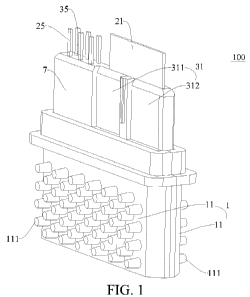
[0026] FIG. 1 is a schematic structural diagram of a power module according to
an
embodiment of the present disclosure;
[0027] FIG. 2 is an assembly view of a power module according to an embodiment
of
the present disclosure;
[0028] FIG. 3 is an exploded view of a power module according to an embodiment
of
the present disclosure;
[0029] FIG. 4 is a cross-sectional view of a power module according to an
embodiment
of the present disclosure;
[0030] FIG. 5 is a cross-sectional view of a first bridge arrn assembly of a
power module
according to an embodiment of the present disclosure;
[0031] FIG. 6 is a cross-sectional view of a second bridge arm assembly of a
power
module according to an embodiment of the present disclosure;
[0032] FIG. 7 is a cross-sectional view at an alternating
current terminal of a power
module according to an embodiment of the present disclosure;
[0033] FIG. 8 is a cross-sectional view at a direct current terminal of a
power module
according to an embodiment of the present disclosure;
[0034] FIG. 9 is a circuit diagram of a power module according to an
embodiment of
the present disclosure;
[0035] FIG. 10 is a cross-sectional view of a first bridge arm assembly of a
power
6
CA 03233289 2024- 3- 27
module according to some other embodiments of the present disclosure;
[0036] FIG. 11 is a circuit diagram of a power module according to some other
embodiments of the present disclosure;
[0037] FIG. 12 is a schematic structural diagram of a power module according
to some
other embodiments of the present disclosure;
[0038] FIG. 13 is a cross-sectional view of a first bridge arm assembly of a
power
module according to some other embodiments of the present disclosure;
[0039] FIG. 14 is a cross-sectional view of a second bridge arm assembly of a
power
module according to some other embodiments of the present disclosure;
[0040] FIG. 15 is a cross-sectional view of a first bridge arm assembly of a
power
module according to some other embodiments of the present disclosure;
[0041] FIG. 16 is a cross-sectional view of a second bridge arm assembly of a
power
module according to some other embodiments of the present disclosure;
[0042] FIG. 17 is a cross-sectional view of a power module according to a
further
embodiment of the present disclosure;
[0043] FIG. lg is a cross-sectional view along A-A in FIG. 17;
[0044] FIG. 19 and FIG. 20 are cross-sectional views of
distribution of a direct current
terminal and an alternating current terminal in two other embodiments of a
power module
according to the present disclosure; and
[0045] FIG. 21 is a cross-sectional view of distribution of a
direct current terminal and
an alternating current terminal from another perspective of the power module
in the embodiment
in FIG. 20.
[0046] Reference numerals:
7
CA 03233289 2024- 3- 27
power module 100,
housing 1, sub-housing 11, pin-fin structure 111,
first bridge arm assembly 2, alternating current terminal 21, first copper
layer 22, first chip
23, first flexible circuit board 24, alternating current control terminal 25,
second bridge arm assembly 3, direct current terminal 31, positive terminal
311, negative
terminal 312, second copper layer 32, positive copper layer region 321,
negative copper layer
region 322, second chip 33, second flexible circuit board 34, direct current
control terminal 35,
flexible control board 41, connection point 42, capacitance absorption region
43, positive
capacitance region 431, negative capacitance region 432, welding block 433,
temperature sensor
44, absorption capacitor 45, pad 46,
first pad block 51, first welding layer 52, second pad block 61, second
welding layer 62,
insulating member 7, first insulating layer 71, second insulating layer 72,
ceramic layer 8.
DETAILED DESCRIPTION
[0047]
The following describes in detail embodiments of the present disclosure,
examples of the embodiments are shown in the accompanying drawings, and
identical or similar
reference numerals represent identical or similar elements or elements having
identical or similar
functions. The following embodiments described with reference to the
accompanying drawings
are examples, and are merely intended to explain the present disclosure, but
should not be
construed as a limitation on the present disclosure.
[0048] A power module 100 according to embodiments of the present disclosure
is
described below with reference to FIG. 1 to FIG. 21. The power module 100 uses
a structural
design in which a direct current terminal 31 and an alternating current
terminal 21 are distributed
8
CA 03233289 2024- 3- 27
in a stacked manner, so that the power module 100 can effectively resolve a
problem that a stray
inductance is large, and running accuracy of the power module 100 is improved.
[0049] As shown in FIG. 1 to FIG. 3, the power module 100 according to
embodiments
of the present disclosure includes a housing 1, a first bridge arm assembly 2,
and a second bridge
arm assembly 3.
[0050]
It should be noted that, as shown in FIG. 1, the housing 1 is
constructed into an
external housing structure of the power module 100, to protect and fasten an
element installed in
the housing 1. In addition, a heat dissipation structure is arranged on each
of two opposite outer
side surfaces of the housing 1. As shown in FIG. 1 and FIG. 2, multiple pin-
fin structures 111 are
used on each outer side surface of the housing 1, to achieve a cooling effect
for a large heat
dissipation area. This helps improve a heat dissipation function for the
element.
[0051] Both the first bridge arm assembly 2 and the second bridge arm assembly
3 are
installed in the housing 1. The inside of the housing 1 is constructed into a
hollow structure, to
form an installation cavity in the housing 1. The installation cavity has an
opening, so that both the
first bridge arm assembly 2 and the second bridge arm assembly 3 are installed
in the installation
cavity. An alternating current terminal 21 of the first bridge arm assembly 2
and a direct current
terminal 31 of the second bridge arm assembly 3 may extend out from the
opening. The first bridge
arm assembly 2 and the second bridge arm assembly 3 are oppositely arranged in
the installation
cavity, and an insulating member 7 is formed between the first bridge arm
assembly 2 and the
second bridge arm assembly 3, so that the insulating member 7 can play an
insulation and
separation role between the first bridge arm assembly 2 and the second bridge
arm assembly 3. in
this way, relative positions of internal elements of the first bridge arm
assembly 2 and the second
bridge arm assembly 3 are kept fixed, both the first bridge arm assembly 2 and
the second bridge
9
CA 03233289 2024- 3- 27
arm assembly 3 are in a stable structural state, and the insulating member 7
can effectively avoid
an accidental short circuit between the first bridge arm assembly 2 and the
second bridge arm
assembly 3, so that running safety of the first bridge arm assembly 2 and the
second bridge arm
assembly 3 is improved.
[0052]
During actual design, the housing 1 may have an integral structure.
Alternatively,
as shown in FIG. 2 and FIG. 3, the housing 1 may be constructed into two sub-
housings 11 in
advance, and side surfaces of the two sub-housings 11 that face each other are
constructed into
concave structures, so that the housing 1 is formed after the two sub-housings
11 are spliced and
fastened, and the installation cavity is formed between the two sub-housings
11. The first bridge
arm assembly 2 may be first installed in a sub-housing 11, and the second
bridge arm assembly 3
may be first installed in the other sub-housing 11. In this way, as shown in
FIG. 2, the first bridge
arm assembly 2 and the sub-housing 11 form a left part of the power module
100, and the second
bridge arm assembly 3 and the other sub-housing 11 form a right part of the
power module 100.
Then, the left part and the right part are spliced to splice the two sub-
housings 11 into a whole.
The first bridge arm assembly 2 and the second bridge arm assembly 3 are
oppositely arranged
between the two sub-housings 11. An installation gap formed between the first
bridge arm
assembly 2 and the second bridge arm assembly 3 may be used as an injection
molding space, to
pot thermosetting resin in the injection molding space, so that the
thermosetting resin forms the
insulating member 7 between the first bridge arm assembly 2 and the second
bridge arm assembly
3 after solidification. in this way, fastening and packaging can be achieved,
and insulative
protection can be achieved. The two sub-housings 11 may form an integral
sealed cavity through
a process such as brazing, laser welding, or stir welding. During welding,
specific pressure may
be applied to the sub-housings 11, so that specific stress is retained to
maintain reliable impact of
CA 03233289 2024- 3- 27
an electrical connection point of an internal chip after the welding is
completed. After the housing
1 is welded, reflow soldering may be performed to melt and bond solder in the
module.
[0053] Therefore, after the power module 100 is packaged and fastened, side
surfaces
of the two sub-housings 11 that face away from each other both have pin-fin
structures 111, so that
the two sub-housings 11 can respectively play a heat dissipation and cooling
role on side surfaces
of the first bridge arm assembly 2 and the second bridge arm assembly 3 that
face away from each
other.
[0054]
As shown in FIG. 1 to FIG. 3. the first bridge arrn assembly 2 has the
alternating
current terminal 21, and the second bridge arm assembly 3 has the direct
current terminal 31. The
alternating current terminal 21 and the direct current terminal 31 are used as
power terminals of
the power module 100, to input or output a current, and ensure that the power
module 100 can run
normally. The alternating current terminal 21 and the direct current terminal
31 may be designed
into a flat structure, and both the alternating current terminal 21 and the
direct current terminal 31
may be made of a copper material, so that the alternating current terminal 21
and the direct current
terminal 31 (which are in indirect contact) can be distributed in a space.
Specifically, a projection
of the alternating current terminal 21 on a plane on which the direct current
terminal 31 is located
at least partially overlaps the direct current terminal 31. in other words,
the alternating current
terminal 21 and the direct current terniinal 31 are oppositely distributed in
thickness directions of
the alternating current terminal 21 and the direct current terminal 31. In
this way, the alternating
current terminal 21 and the direct current terminal 31 can be arranged in the
power module 100
together while ensuring current conduction of the alternating current terminal
21 and the direct
current terminal 31, and at least a part of the insulating member 7 can be
arranged between the
alternating current terminal 21 and the direct current terminal 31, so that an
internal installation
11
CA 03233289 2024- 3- 27
space is utilized to a greatest extent, and a current short circuit between
the direct current terminal
31 and the alternating current terminal 21 is effectively avoided. Certainly,
in the present disclosure,
the at least a part of the insulating member 7 located between the alternating
current terminal 21
and the direct current terminal 31 may use an injection molding or filling
resin material, or may
use a thin-film material made of an insulating material such as a polyimide
film or a ceramic
insulating sheet. This also facilitates an insulating function between the
alternating current terminal
21 and the direct current terminal 31. A thickness of the thin-film material
may be designed to be
0.1 mm to 0.3 mm.
[0055]
In addition, it should be noted that, the alternating current terminal
21 and the
direct current terminal 31 are oppositely installed in the power module 100,
and the direct current
terminal 31 may include a positive terminal 311 and a negative terminal 312.
in this way, after the
positive ten-ninal 311, the negative terminal 312, and the alternating current
terminal 21 are
oppositely distributed, a stray inductance of the terminal can be reduced.
Specifically, according
to this design, the positive terminal 311, the negative terminal 312, and the
alternating current
terminal 21 can be closely attached to provide a closest return path for a
current, and a commutated
current between positive and negative electrodes can induct a reverse current
on the closely
attached alternating current terminal 21 to reduce an inductance of a
commutating circuit, so that
a stray inductance is effectively reduced.
[0056] According to the power module 100 in embodiments of the present
disclosure, a
structural design in which the alternating current terminal 21 of the first
bridge arm assembly 2
and the direct current terminal 31 of the second bridge arm assembly 3 are
stacked in an insulative
manner enables the power module 100 to effectively resolve a problem that a
stray inductance is
large, so that running accuracy of the power module 100 is improved.
12
CA 03233289 2024- 3- 27
[0057] In some embodiments, as shown in FIG. 3 and FIG. 5, the first bridge
arm
assembly 2 further includes a first copper layer 22 and a first chip 23. A
projection of the first
copper layer 22 on a plane on which the alternating current terminal 21 is
located at least partially
overlaps the alternating current terminal 21, and the first chip 23 is
installed in the alternating
current terminal 21, so that the first chip 23 is electrically connected to
the alternating current
terrninal 21, and the first chip 23 and the first copper layer 22 are
distributed directly facing each
other. As shown in FIG. 3 and FIG. 5, a lower part of the alternating current
terminal 21 is
constructed to have a groove structure, and the first chip 23 is installed in
the groove structure, so
that a relative position between the first chip 23 and the alternating current
terminal 21 is kept
fixed. The first copper layer 22 fits the lower part of the alternating
current terminal 21 and fits a
side surface of the first chip 23, so that the first copper layer 22, the
first chip 23, and the alternating
current terminal 21 are relatively fastened.
[0058]
As shown in FIG. 3 and FIG. 5, there are three first chips 23, and the
alternating
current terminal 21 has three groove structures. The three first chips 23 are
correspondingly
installed in the three groove structures respectively, so that the three first
chips 23 are all relatively
fastened to the alternating current terminal 21, and the three first chips 23
are all distributed directly
facing the first copper layer 22.
[0059] As shown in FIG. 3 and FIG. 6, the second bridge arm assembly 3 further
includes a second copper layer 32 and a second chip 33. A projection of the
second copper layer
32 on the plane on which the direct current terminal 31 is located at least
partially overlaps the
direct current terminal 31, and the second chip 33 is installed in the direct
current terminal 31, so
that the second chip 33 is electrically connected to the direct current
terminal 31, and the second
chip 33 and the second copper layer 32 are distributed directly facing each
other. As shown in FIG.
13
CA 03233289 2024- 3- 27
3 and FIG. 6, a lower part of the direct current terminal 31 is constructed to
have a groove structure,
and the second chip 33 is installed in the groove structure, so that a
relative position between the
second chip 33 and the direct current terminal 31 is kept fixed. The second
copper layer 32 fits the
lower part of the direct current terminal 31 and fits a side surface of the
second chip 33, so that the
second copper layer 32, the second chip 33, and the direct current terminal 31
are relatively
fastened.
[0060] As shown in FIG. 3 and FIG. 6, there are three second
chips 33, and the direct
current terminal 31 has three groove structures. The three second chips 33 are
correspondingly
installed in the three groove structures respectively, so that the three
second chips 33 are all
relatively fastened to the direct current terminal 31, and the three second
chips 33 are all distributed
directly facing the second copper layer 32.
[0061] In addition, during specific design, the direct current
terminal 31 includes the
positive terminal 311 and the negative terminal 312, and the second copper
layer 32 includes a
positive copper layer region 321 and a negative copper layer region 322. The
positive copper layer
region 321 and the negative copper layer region 322 are spaced apart. The
positive copper layer
region 321 is configured to be stacked with the positive terminal 311, and the
negative copper layer
region 322 is configured to be stacked with the negative terminal 312.
[0062] It should be noted that, as shown in FIG. 3, a ceramic layer 8 is
arranged between
the first copper layer 22 and a left sub-housing 11, to space the first copper
layer 22 from the sub-
housing 11 in an insulative manner. In addition, a ceramic layer 8 is arranged
between the second
copper layer 32 and a right sub-housing 11, to space the second copper layer
32 from the other
sub-housing 11 in an insulative manner. in this way, it is ensured that an
internal electronic element
of the power module 100 is spaced from the housing 1 in an insulative manner.
14
CA 03233289 2024- 3- 27
[0063] In some embodiments, as shown in FIG. 4, a first pad block 51 is
arranged
between the first chip 23 and the second copper layer 32, and adjacent two of
the first copper layer
22, the first chip 23, the first pad block 51, and the second copper layer 32
are welded and fastened
by a first welding layer 52. In other words, when the first bridge arm
assembly 2 and the second
bridge arm assembly 3 are actually installed, the first chip 23 may be first
installed in the groove
structure of the alternating current terminal 21, the first chip 23 and the
first copper layer 22 are
welded and fastened, and then the first pad block 51 is welded and fastened
between the first chip
23 and the second copper layer 32. in this way, adjacent two of the first
copper layer 22, the first
chip 23, the first pad block 51, and the second copper layer 32 are welded and
fastened.
[0064] Similarly, as shown in FIG. 4, a second pad block 61 is arranged
between the
second chip 33 and the first copper layer 22, and adjacent two of the second
copper layer 32, the
second chip 33, the second pad block 61, and the first copper layer 22 are
welded and fastened by
a second welding layer 62. in other words, during specific installation, the
second chip 33 may be
first installed in the groove structure of the direct current terminal 31, the
second chip 33 and the
second copper layer 32 are welded and fastened, and then the second pad block
61 is welded and
fastened between the second chip 33 and the first copper layer 22. In this
way, adjacent two of the
second copper layer 32, the second chip 33, the second pad block 61, and the
first copper layer 22
are welded and fastened.
[0065]
Therefore, the first chip 23 and the second chip 33 in the present
disclosure have
a reverse installation relationship. This can help reduce usage of bridgeware,
so that structure
design costs are reduced. in addition, a copper foil arranged at a lower layer
is a complete
conducting region, and can provide a smooth return path for a current. This
helps reduce a stray
inductance.
CA 03233289 2024- 3- 27
[0066] In some embodiments, each of the direct current terminal 31 and the
alternating
current terminal 21 is constructed into a platelike structure. In other words,
during specific molding,
each of the positive terminal 311, the negative terminal 312, and the
alternating current terminal
21 may be formed into a specified shape through a stamping or cutting process.
As shown in FIG.
3, each of the direct current terrninal 31 and the alternating current
terminal 21 is stamped to form
a plate shape with multiple groove structures. Groove structures of the direct
current terminal 31
and the alternating current terminal 21 are distributed in a staggered manner.
Then, the alternating
current terminal 21 and the first copper layer 22 are stacked and connected
through welding, and
the direct current terminal 31 and the second copper layer 32 are stacked and
connected through
welding.
[0067]
According to this design, overcun-ent capabilities or the first copper
layer 22 and
the second copper layer 32 can be enhanced, to avoid using a thick copper
layer, so as to avoid a
stress problem. In addition, a spacing between a circuit (direct current
positive and negative end
circuits) of an alternating current circuit board and a circuit (alternating
current end circuit) of a
direct current circuit board can be reduced, to enhance mutual coupling, so
that a current return
path is the closest. An advantage is that a current return inductance is
reduced, and a conductive
frame including the thick direct current terminal 31 and alternating current
terminal 21 can provide
a good current equalization effect.
[0068] In some embodiments, as shown in FIG. 5, the first bridge arm assembly
2 further
includes a first flexible circuit board 24 and an alternating current control
terminal 25. The first
flexible circuit board 24 is electrically connected between the first chip 23
and the alternating
current control terminal 25. The alternating current control terminal 25
extends out of the housing
1. In this way, a control signal generated at the first chip 23 can be
transferred to the alternating
16
CA 03233289 2024- 3- 27
current control terminal 25 through the first flexible circuit board 24, and
then output to the outside
of the power module 100 through the alternating current control terminal 25,
to facilitate receiving
and obtaining by a worker.
[0069] As shown in FIG. 5, the first flexible circuit board 24
has three chip lead-out
points, and the three chip lead-out points of the first flexible circuit board
24 are respectively
configured to be electrically connected to the three first chips 23. In
addition, the alternating
current control terminal 25 may be constructed into three spaced signal
terminals, and the three
signal terminals are respectively Ti, Gl, and Si. The three signal terminals
are spaced in parallel
and extend out from an open end of the installation cavity. This facilitates
output of the control
signal.
[0070] As shown in FIG. 7, a gap structure is Conned at the
edge or the first copper layer
22. A pad 46 of the alternating current control terminal 25 is arranged at the
gap structure. The pad
46 is divided into three parts. in this way, the three signal terminals can be
welded and fastened to
the three parts of the pad 46 respectively.
[0071] As shown in FIG. 6, the second bridge arm assembly 3 further includes a
second
flexible circuit board 34 and a direct current control terminal 35. The second
flexible circuit board
34 is electrically connected between the second chip 33 and the direct current
control terminal 35.
The direct current control terminal 35 extends out of the housing 1. In this
way, a control signal
generated at the second chip 33 can be transferred to the direct current
control terminal 35 through
the second flexible circuit board 34, and then output to the outside of the
power module 100
through the direct current control terminal 35, to facilitate receiving and
obtaining by a worker.
[0072] As shown in FIG. 6, the second flexible circuit board
34 has three chip lead-out
points, and the three chip lead-out points of the second flexible circuit
board 34 are respectively
17
CA 03233289 2024- 3- 27
configured to be electrically connected to the three second chips 33. In
addition, the direct current
control terminal 35 may be constructed into three spaced signal terminals, and
the three signal
terminals are respectively T2, G2, and S2. The three signal terminals are
spaced in parallel and
extend out from the open end of the installation cavity. This facilitates
output of the control signal.
[0073] As shown in FIG. 8, the positive copper layer region
321 and the negative copper
layer region 322 are spaced, and a gap structure is formed at the edge of the
positive copper layer
region 321. A pad 46 of the direct current control terminal 35 is arranged at
the gap structure. The
pad 46 is divided into three parts. in this way, the three signal terminals
can be welded and fastened
to the three parts of the pad 46 of the direct current control terminal 35
respectively.
[0074] It should be noted that, in the present disclosure,
both the direct current circuit
board and the alternating current circuit board are flexible circuit boards,
so that when connecting
a control end and a gate control end of a chip, the flexible circuit board can
replace a conventional
binding process. In this way, a structural characteristic that the flexible
circuit board has a planar
structure and has an insulating layer with sufficient strength can be used,
and there is no need to
reserve a large radian space and insulating spacing for the binding process.
In addition, this helps
reduce a module thickness and reduce a stray inductance.
[0075] In some embodiments, the alternating current control terminal 25 and
the direct
current control terminal 35 are constructed into a shared flexible control
board 41. In other words,
in the embodiments. a design with three independent pins is not used for the
alternating current
control terminal 25 and the direct current control tenuinal 35, but the same
flexible control board
41 is used to output a control signal.
[0076] Specifically, as shown in FIG. 15, four connection
points 42 are provided on the
first flexible circuit board 24. in addition, as shown in FIG. 16, four
connection points 42 are also
18
CA 03233289 2024- 3- 27
provided on the second flexible circuit board 34. A shared flexible control
board 41 is arranged.
Four connection points 42 are correspondingly provided on the flexible control
board 41. The four
connection points 42 on the flexible control board 41 are respectively
connected to the four
connection points 42 on the first flexible circuit board 24, and are
respectively connected to the
four connection points 42 on the second flexible circuit board 34, to output a
control signal.
[0077] Alternatively, in some other embodiments, the
alternating current control
terminal 25 and the direct current control terminal 35 are separately
constructed into flexible
control boards 41. As shown in FIG. 13, an upper end of the alternating
current control terminal
25 extends upward and extends out of the installation cavity. To be specific,
an upper end extension
part of the alternating current control terminal 25 is constructed into a
flexible control board 41
corresponding to the alternating current control terminal 25, to output an
electrical control signal
on the alternating current control terminal 25. In addition, as shown in FIG.
14, an upper end of
the direct current control terminal 35 extends upward and extends out of the
installation cavity. To
be specific, an upper end extension part of the direct current control
terminal 35 is constructed into
a flexible control board 41 corresponding to the direct current control
terminal 35, to output an
electrical control signal on the direct current control terminal 35.
[0078] Therefore, the alternating current control terminal 25
and the direct current
control terminal 35 are constructed into the flexible control boards 41, to
further extend from the
flexible circuit boards to the outside of the power module 100. A design of a
flexible control
terminal is implemented, and there is a function that a structure is more
compact and a spaced is
saved. in addition, an interface position of a drive board is more flexibly
set. The flexible control
board 41 may perform impedance control on a gate control signal, to provide a
channel design for
ensuring signal integrity. This cannot be achieved by a pin-type terminal. In
addition, it can be
19
CA 03233289 2024- 3- 27
ensured that a gate motion signal does not generate distortion such as
overshoot or ringing. in other
words, reliable turn-off or turn-on of a high-speed component SiC MOSFET can
be ensured, and
a loss can be reduced.
[0079] In some embodiments, as shown in FIG. 17, the direct current terminal
31
includes a positive terminal 311 and a negative terminal 312 that are spaced
apart. The second
flexible circuit board 34 has a capacitance absorption region 43, and two ends
of the capacitance
absorption region 43 are electrically connected to the negative terminal 312
and the positive
terminal 311 respectively. in this way, arrangement of the capacitance
absorption region 43 enables
the capacitance absorption region 43 to effectively absorb overshoot energy
generated by a stray
inductance during a switching action. in addition, a system EMT
(electromagnetic interference)
problem can be optimized. During specific design, a quantity of layers of the
capacitance
absorption region 43 may be set according to an actual requirement.
[0080]
As shown in FIG. 18, the capacitance absorption region 43 includes a
positive
capacitance region 431 and a negative capacitance region 432. The positive
terminal 311 and the
positive capacitance region 431 are welded and connected through a welding
block 433, and the
negative terminal 312 and the negative capacitance region 432 are welded and
connected through
a welding block 433. The positive capacitance region 431 corresponding to the
positive terminal
311 and the negative capacitance region 432 corresponding to the negative
terminal 312 are
distributed in a stacked manner, to further restrict a turn-off peak, reduce a
loop, and reduce EMI
(electromagnetic interference).
[0081] In some embodiments, a temperature sensor 44 is arranged on the first
flexible
circuit board 24 and/or the second flexible circuit board 34. As shown in FIG.
5, the temperature
sensor 44 is designed on the first flexible circuit board 24, to detect a
temperature of the first
CA 03233289 2024- 3- 27
flexible circuit board 24 through the temperature sensor 44. Specifically, a
hollow design is used
in the first flexible circuit board 24, to install the temperature sensor 44
in a hollow region of the
first flexible circuit board 24 to fasten the temperature sensor 44.
Similarly, as shown in FIG. 6,
the temperature sensor 44 is designed on the second flexible circuit board 34,
to detect a
temperature of the second flexible circuit board 34 through the temperature
sensor 44. Specifically,
a hollow design is used in the second flexible circuit board 34, to install
the temperature sensor 44
in a hollow region of the second flexible circuit board 34 to fasten the
temperature sensor 44.
Certainly, the temperature sensor 44 may be designed on each of the first
flexible circuit board 24
and the second flexible circuit board 34, to separately detect temperatures of
the two circuit boards.
[0082] In some embodiments, the direct current terminal 31
includes the positive
terminal 311 and the negative terminal 312. A projection of each of the
positive terminal 311 and
the negative terminal 312 on the plane on which the alternating current
terminal 21 is located at
least partially overlaps the alternating current terminal 21. In other words,
in a thickness direction
of the alternating current terminal 21, both the positive terminal 311 and the
negative terminal 312
are distributed opposite the alternating current terminal 21. In this way,
after the positive terminal
311, the negative terminal 312, and the alternating current terminal 21 are
oppositely distributed,
a stray inductance of the terminal can be reduced. Specifically, according to
this design, the
positive terminal 311, the negative terminal 312, and the alternating current
terminal 21 can be
closely attached to provide a closest return path for a current, and a
commutated current between
positive and negative electrodes can induct a reverse current on the closely
attached alternating
current terminal 21 to reduce an inductance of a commutating circuit, so that
a stray inductance is
effectively reduced.
[0083] It should be noted that, during specific installation,
the positive terminal 311, the
21
CA 03233289 2024- 3- 27
negative terminal 312, and the alternating current terminal 21 may be arranged
in multiple manners,
and each manner can reduce a stray inductance.
[0084] In some embodiments, as shown in FIG. 2, both the positive terminal 311
and
the negative terminal 312 are stacked on a first side of the insulating member
7. The positive
terminal 311 and a part of the insulating member 7 are stacked. The negative
terminal 312 and
another part of the insulating member 7 are stacked. The alternating current
terminal 21 is stacked
on a second side of the insulating member 7. in other words, both the positive
terminal 311 and
the negative terminal 312 are located on the same side of the insulating
member 7, and the
alternating current terminal 21 is located on another side of the insulating
member 7. In this way,
the two direct current terminals 31: the positive terminal 311 and the
negative terminal 312, and
the alternating current terminal 21 are respectively arranged on two sides of
the insulating member
7, so that a stacked distribution of the direct current terminal 31 and the
alternating current terminal
21 can be achieved. This helps reduce a stray inductance.
[0085] Alternatively, in some embodiments, the insulating
member 7 includes a first
insulating layer 71 and a second insulating layer 72. The positive terminal
311 is located on a first
side of the alternating current terminal 21. The first insulating layer 71 is
arranged between the
positive terminal 311 and the alternating current terminal 21. The negative
terminal 312 is located
on a second side of the alternating current terminal 21. The second insulating
layer 72 is arranged
between the negative terminal 312 and the alternating current terminal 21.
Positions of the positive
terminal 311 and the negative terminal 312 may be interchanged for
installation.
[0086] During specific design, as shown in FIG. 1 9, the first
insulating layer 71 and the
second insulating layer 72 are spaced apart. The positive terminal 311 may be
arranged on a left
side of the alternating current terminal 21, and the negative terminal 312 may
be arranged on a
??
CA 03233289 2024- 3- 27
right side of the alternating current terminal 21. In addition, the first
insulating layer 71 is arranged
between the positive terminal 311 and the alternating current terminal 21 to
implement insulative
spacing. The second insulating layer 72 is arranged between the negative
terminal 312 and the
alternating current terminal 21 to implement insulative spacing. in this way,
a stacked distribution
of the direct current terminal 31 and the alternating current terminal 21 can
be achieved. This helps
reduce a stray inductance.
[0087] Alternatively, in some embodiments, the insulating
member 7 includes a first
insulating layer 71 and a second insulating layer 72. As shown in FIG. 20, the
positive terminal
311, the negative terminal 312, and the alternating current terminal 21 are
sequentially distributed.
For example, the positive terminal 311 is located on the leftmost side, the
alternating current
terminal 21 is located on the rightmost side, and the negative terminal 312 is
located between the
positive terminal 311 and the alternating current terminal 21. in addition,
the first insulating layer
71 is arranged between the positive terminal 311 and the negative terminal
312, and the second
insulating layer 72 is arranged between the negative terminal 312 and the
alternating current
terrninal 21. In other words, the positive terminal 311, the first insulating
layer 71, the negative
terminal 312, the second insulating layer 72, and the alternating current
terminal 21 are
sequentially stacked. In this way, a stacked distribution of the direct
current terminal 31 and the
alternating current terminal 21 can be achieved. This helps reduce a stray
inductance.
[0088] Alternatively, the negative terminal 312, the positive
terminal 311, and the
alternating current terminal 21 may be sequentially distributed. For example,
the negative terminal
312 is located on the leftmost side, the alternating current terminal 21 is
located on the rightmost
side, and the positive terminal 311 is located between the negative terminal
312 and the alternating
current terminal 21. In addition, the first insulating layer 71 is arranged
between the negative
23
CA 03233289 2024- 3- 27
terminal 312 and the positive terminal 311, and the second insulating layer 72
is arranged between
the positive terminal 311 and the alternating current terminal 21. In other
words, the negative
terminal 312, the first insulating layer 71, the positive terminal 311, the
second insulating layer 72,
and the alternating current terminal 21 are sequentially stacked. in this way,
a stacked distribution
of the direct current terminal 31 and the alternating current terminal 21 can
be achieved. This helps
reduce a stray inductance.
[0089] During specific design, as shown in FIG. 21, the insulating member 7
may be
constructed to have three installation slots. The three installation slots are
sequentially distributed
in a thickness direction of the insulating member 7. The alternating current
terminal 21 is installed
in the first installation slot. The negative terminal 312 has a negative
plugging part, and the
negative plugging part is plugged into a middle installation slot. The
positive terminal 311 has a
positive plugging part, and the positive plugging part is plugged into the
other installation slot.
Therefore, an insulating part between the first installation slot and the
middle installation slot is
the second insulating layer 72, and an insulating part between the middle
installation slot and the
other installation slot is the first insulating layer 71.
[0090]
In other words, the alternating current terminal 21, the positive
terminal 311, and
the negative terminal 312 in the present disclosure may cooperate with the
insulating member 7 in
multiple forms, and each form can implement a stacked cooperation between the
direct current
terminal 31 and the alternating current terminal 21, that is, each form can
reduce a stray inductance.
[0091] In some embodiments, as shown in FIG. 19 or FIG. 20, an overall
extension
length of the alternating current terminal is greater than an overall
extension length of the direct
current terminal 31. in this way, it can be ensured that the direct current
terminal 31 obtains a
whole-process magnetic field cancellation function. A part of the alternating
current terminal 21
24
CA 03233289 2024- 3- 27
that falls outside a plastic package provides an electrical connection point.
The direct current
terminal 31 may be polished after injection molding, to expose an electrical
connection surface, or
may be molded at a time through a particular mold design. A protrusion made of
an insulating
material is arranged between the positive terminal 311 and the negative
terminal 312 to ensure a
sufficient creepage distance.
[0092] In some embodiments, as shown in FIG. 10, the direct current terminal
31
includes the positive terminal 311 and the negative terminal 312. An
absorption capacitor 45 is
arranged between the positive terminal 311 and the negative terminal 312, so
that the absorption
capacitor 45 absorbs overshoot energy generated by a stray inductance during a
switching action.
In addition, a system EMI (electromagnetic interference) problem can be
optimized.
[0093] It should be noted that, the power module 100 in the present disclosure
may be
processed and molded through the following process:
[0094]
The first chip 23, the second chip 33, the first flexible circuit board
24, the second
flexible circuit board 34, the housing 1, the alternating current control
terminal 25, the direct
current control terminal 35, the alternating current terminal 21, the positive
terminal 311, the
negative terminal 312, the first pad block 51, and the second pad block 61 are
first welded through
silver sintering or a conventional brazing process. Then, the pad, the first
chip 23, and the second
chip 33 are positioned. A GS electrode of the chip is led out through a
process such as ultrasonic
welding, soldering, or brazing. In addition, the same processing is performed
for welding between
the first flexible circuit board 24, the second flexible circuit board 34, and
the pad.
[0095] In addition, at a place, for example, the temperature sensor in some
embodiments
of the present disclosure, at which the first flexible circuit board 24 and
the second flexible circuit
board 34 generate an electrical connection, the two flexible circuit boards
need to be connected to
CA 03233289 2024- 3- 27
form a loop. In the present disclosure, pads are arranged at corresponding
positions on the first
flexible circuit board 24 and the second flexible circuit board 34, and an
elastic material is padded
at the bottom of a pad on one of the flexible circuit boards, to ensure that
an initial crimping force
is provided after snap-fit between the first copper layer 22 and the second
copper layer 32, so as
to ensure reliable contact during welding. The first copper layer 22 and the
second copper layer 32
are first respectively bonded to the two sub-housings 11 through a low-
temperature eutectic
process. In this way, production of the first bridge arm assembly 2 and the
second bridge arm
assembly 3 is completed. Then, solder is painted on a contact surface between
the housing 1 and
each of the first bridge arm assembly 2 and the second bridge arm assembly 3
and a welding
surface between the ceramic layer 8 and each of the two pad blocks. After snap-
fit between the
first bridge arm assembly 2 and the second bridge arm assembly 3, housing
sealing and internal
electrical connection are completed through a process such as reflow
soldering. Then,
thermosetting resin is poured, so that production of the power module 100 is
completed.
[0096] The present disclosure further provides an electrical
device, which includes the
power module 100 according to any of the foregoing embodiments. Arranging the
power module
100 can effectively resolve a problem that a stray inductance is large, so
that running accuracy of
the power module 100 is improved.
[0097] In the description of the present disclosure, it should
be understood that
orientation or position relationships indicated by the terms such as "center",
"longitudinal",
"transverse", "length", "width", "thickness", "above", "below", "front",
"back", "left", "right",
"vertical", "horizontal'', "top", "bottom", "inside", "outside", "clockwise",
"anticlockwise", "axial
direction", "radial direction", and "circumferential direction" are based on
orientation or position
relationships shown in the accompanying drawings, and are merely used for ease
and brevity of
26
CA 03233289 2024- 3- 27
description of the present disclosure, rather than indicating or implying that
the indicated apparatus
or element needs to have a particular orientation or needs to be constructed
and operated in a
particular orientation. Therefore, such terms should not be construed as a
limitation on the present
disclosure.
[0098] In the description of the present disclosure, a "first
feature" or "second feature"
may include one or more of the features.
[0099] In the description of the present disclosure, "multiple"
means two or more.
[0100] In the description of the present disclosure, that a
first feature is "above" or
"below" a second feature may include that the first and second features are in
direct contact, or
may include that the first and second features are not in direct contact but
are in contact by using
other features therebetween.
[0101] In the description of the present disclosure, that a
first feature is "above", "over",
or "on" a second feature includes that the first feature is right above and on
the inclined top of the
second feature or merely indicates that a level of the first feature is higher
than that of the second
feature.
[0102] In the description of this specification, descriptions
using reference terms "an
embodiment", "some embodiments". "an example embodiment", "an example", "a
specific
example", or "some examples" mean that specific features, structures,
materials, or characteristics
described with reference to the embodiment or example are included in at least
one embodiment
or example of the present disclosure. in this specification, example
descriptions of the foregoing
terms do not necessarily refer to the same embodiment or example. In addition,
the described
specific features, structures, materials, or characteristics may be combined
in a proper manner in
any one or more embodiments or examples.
77
CA 03233289 2024- 3- 27
[0103] Although embodiments of the present disclosure have been shown and
described,
a person of ordinary skill in the art should understand that various changes,
modifications,
replacements, and variations may be made to the embodiments without departing
from the
principle and purpose of the present disclosure, and the scope of the present
disclosure is defined
by the claims and their equivalents.
28
CA 03233289 2024- 3- 27