Note: Descriptions are shown in the official language in which they were submitted.
WO 2023/101702
PCT/US2021/072652
INTERPOSER FOR SEMICONDUCTOR-BASED SINGLE PHOTON
EMISSION COMPUTED TOMOGRAPHY DETECTOR
BACKGROUND
[0001] The present embodiments relate to semiconductor
detectors for
single photon emission computed tomography (SPECT). Current detectors
are tested before attachment to electronics. The only tests are pre-contact
attachment, which manufacturers of semiconductor detectors use as a basis
to qualify detectors for use in different applications. Carrier boards with
connectors are attached to detectors without confirmation whether the
detectors have additional problems caused by intermediary steps or in
interaction with the carrier and electronics. This is not an issue today,
since
test fixtures used to qualify detectors have connectors and the cost of
replacing these detectors is not significant ¨ even if problems exist.
[0002] A more severe issue occurs when the package is fully
integrated,
such that the detector and an application specific integrated circuit (ASIC)
are
assembled into a compact and indivisible unit. The semiconductor detectors
are not tested post-contact attachment when using direct-attachment
technology. There is no confirmation that the detector is performing as
required post attachment. If not operating correctly, the entire assembly,
including the ASIC, must be discarded.
SUMMARY
[0003] By way of introduction, the preferred embodiments
described below
include methods and systems for testing or production of a semiconductor-
based detector in SPECT. An interposer, such as elastomeric device with
conductors, is sandwiched between a carrier and the semiconductor detector.
The conductors allow for temporary separate connections of detector
electrodes to signal processing circuitry, providing for testing of the
detector
operating with the signal processing circuitry. The interposer provides
separate electrical connections for testing but may also be used in a final,
fully
integrated detector for use in a SPECT system.
[0004] In a first aspect, a SPECT detector system includes a
SPECT
detector, which is a semi-conductor with first conductors exposed on a first
CA 03236859 2024- 4- 30
WO 2023/101702
PCT/US2021/072652
detector surface. A carrier has an attached signal processing circuit and
second conductors exposed on a first carrier surface. An interposer is
between the first surface of the SPECT detector and the second surface of
the carrier. The interposer has third conductors extending between first and
second interposer surfaces. The third conductors electrically connect the
first
conductors with the second conductors in separate electrical paths for
separate detection cells of the SPECT detector.
[0005] In one embodiment, the SPECT detector is a pixelated
detector
where the first conductors are electrically isolated electrodes for the
separate
detection cells. The carrier is a printed circuit board. The signal processing
circuit is an application specific integrated circuit.
[0006] In another embodiment, the interposer is in asperity
contact free of
bonding with the SPECT detector. For example, the carrier is in a test rig
with
the SPECT detector removably stacked with the interposer on the carrier in a
testing arrangement. In another embodiment, the SPECT detector is bonded
to the interposer, and the interposer is bonded to the carrier.
[0007] In yet another embodiment, the interposer is an array
of the third
conductors separated by an elastomer.
[0008] In other embodiments, the separate electrical paths are
a 1-to-1
arrangement of the detection cells to pads on the carrier without shorting
between any of the detection cells. A standard interposer or elastomeric
device may be used by providing a mask on the first interposer surface. The
mask exposes the third conductors for the 1-to-1 arrangement. For example,
the mask is a dielectric of electrically insulating strips forming interposer
cells
exposing the third conductors at a pitch of the detection cells. The
electrically
insulating strips have a width accommodating a tolerance stack-up.
[0009] In some embodiments, the third conductors are curved
wires within
the interposer. In other embodiments, the third conductors are straight wires
within the interposer.
[0010] In an embodiment, the interposer is a plate where the
first and
second interposer surfaces are parallel largest surfaces of the plate.
[0011] In a second aspect, a method is provided for testing a
semiconductor sensor of a gamma camera. The semiconductor sensor is
2
CA 03236859 2024- 4- 30
WO 2023/101702
PCT/US2021/072652
placed onto an elastomeric-conductor plate in a test rig. The semiconductor
sensor is pressed against the elastomeric-conductor plate. The
semiconductor sensor is exposed to gamma radiation. Operation of the
semiconductor sensor for sensing the gamma radiation is tested using signals
from a detector circuit electrically connected to the semiconductor sensor
through elastomeric-conductor plate.
[0012] In one embodiment, pressing forms pixelated electrical
paths from
detector cell electrodes of the semiconductor sensor to pads of a printed
circuit board attached to the detector circuit. Detection from the individual
detector cells is tested.
[0013] The operation of the semiconductor sensor, the detector
circuit, and
a printed circuit board together are tested. The printed circuit board
physically
connects to the detector circuit, but the semiconductor sensor may be
disconnected. For example, the testing is performed without the
semiconductor sensor being bonded to the elastomeric-conductor plate.
[0014] In a third aspect, a SPECT system includes a housing
forming a
patient region and a gamma camera adjacent the patient region. The gamma
camera is a semiconductor detector, a carrier having an attached signal
processing circuit, and an elastomeric device in direct contact with and
between the carrier and the semiconductor detector. The elastomeric device
has electrically isolated conductors electrically connecting electrodes of the
semiconductor detector to pads of the carrier.
[0015] In one embodiment, the carrier is a printed circuit
board, the signal
processing circuit is an application specific integrated circuit, and the
elastomeric device has a dielectric mask exposing the electrically isolated
conductors on a surface of the elastomeric device.
[0016] In another embodiment, the semiconductor, carrier, and
elastomeric
device are pressed together without bonding. In other embodiments, the
semiconductor detector is a pixelated detector of detection cells with
separate
ones of the electrodes for separate ones of the detection cells. The pads of
the carrier connect with electrically isolated traces to separate inputs of
the
signal processing circuit, and the elastomeric device is a plate of the
isolated
conductors and elastomeric material.
3
CA 03236859 2024- 4- 30
WO 2023/101702
PCT/US2021/072652
[0017] The present invention is defined by the following
claims, and
nothing in this section should be taken as a limitation on those claims.
Further aspects and advantages of the invention are discussed below in
conjunction with the preferred embodiments and may be later claimed
independently or in combination.
BRIEF DESCRIPTION OF THE DRAWINGS
[0018] The components and the figures are not necessarily to
scale,
emphasis instead being placed upon illustrating the principles of the
invention.
Moreover, in the figures, like reference numerals designate corresponding
parts throughout the different views.
[0019] Figure 1 illustrates one embodiment of a SPECT detector
assembly, such as for testing;
[0020] Figure 2 illustrates an example testing rig using an
interposer;
[0021] Figure 3 shows different example wire shapes in the
interposer;
[0022] Figure 4 illustrates example electrical path
connections;
[0023] Figure 5 shows an example mask on an interposer;
[0024] Figure 6 is cross-section view of a SPECT imager or
system; and
[0025] Figure 7 is a flow chart diagram of an example
embodiment of a
method for testing a semiconductor detector for SPECT use.
DETAILED DESCRIPTION OF THE DRAWINGS AND PRESENTLY
PREFERRED EMBODIMENTS
[0026] A multi-module post-contact test fixture is provided
for pixelated
semiconductor detectors. Ultra-high performance next generation of SPECT
systems will be based on semiconductor pixelated detectors using direct-
attachment technology. The semiconductor detectors attach directly into the
same PCB substrate where the ASIC is located to minimize trace lengths and
parasitic capacitances, thus improving spectral performance beyond what is
possibly achievable using connectors and multiple carrier and interposer
boards stacked vertically. For testing, the direct contact between the carrier
with the pre-attached ASIC to the sensor is through the interposer or a post-
contact attachment. The interposer with pixelated electrical paths can be
used as a test fixture to validate and/or sort sensors of different grades pre-
4
CA 03236859 2024- 4- 30
WO 2023/101702
PCT/US2021/072652
attachment of the sensor to the carrier and/or to attach the sensor to the
carrier (i.e., replace the sensor attachment step) in a production and
commercial setting.
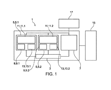
[0027] Figure 1 shows one embodiment of a SPECT detector
system 120.
The SPECT detector system 120 is used for testing a semiconductor detector
102, such as after initial tests and just before forming a production detector
for
use as a gamma camera in a SPECT imaging system. Alternatively, the
SPECT detector system 120 is used as a production detector as assembled in
a SPECT imaging system.
[0028] The SPECT detector system 120 includes a SPECT detector 102,
an interposer 106, and a carrier 107 with a signal processing circuit 104.
This
stack of detector 102, interposer 106, and carrier 107 may be positioned in a
frame, such as between a base (e.g., printed circuit board for electronics or
signal routing) 108 and a force applicator 114 (e.g., pressure plate). Other
frames may be used. Additional, different, or fewer components may be
provided, such as just having the stack of detector 102, interposer 106, and
carrier 107.
[0029] The SPECT detector 102 is a semiconductor. The detector
102 is a
solid-state detector. Any material may be used, such as SI, CZT, CdTe,
and/or other material. The SPECT detector 102 is created with wafer
fabrication at any thickness, such as about 4 mm for CZT. Any size may be
used, such as about 5x5 cm. Figure 1 shows a square shape for the detector
102. Other shapes than square may be used, such as rectangular or
hexagonal.
[0030] The SPECT detector 102 is designed and configured to
detect
gamma emissions, such as emissions from a patient. For example, the
semiconductor is formed as an array of silicon photon multiplier cells.
[0031] The SPECT detector 102 is a pixelated detector. The SPECT
detector 102 forms an array of sensors. For example, the 2.5x2.5 cm or 5x5
cm detector 102 is a 11x11 or 21x21 pixel array of detection cells with a
pixel
pitch of about 2.2 mm. Each detection cell of the array may separately detect
an emission event. Other numbers of pixels, pixel pitch, and/or size of arrays
CA 03236859 2024- 4- 30
WO 2023/101702
PCT/US2021/072652
may be used. Other grids than rectangular may be used, such as a
hexagonal distribution of pixels or detection cells.
[0032] Anode and cathode electrodes are provided on opposite
surfaces of
the detector 102. In the example herein, the lower voltage (e.g., 10 volts or
less) anode electrodes 110 are used. The same or similar arrangement may
be used for cathode electrodes, such as connecting the cathode electrodes
through an interposer to a carrier for a high voltage processing circuit.
Wires
or flex circuit with traces may be used for signal routing from cathode
electrodes where a common processing circuit 104 operates on both anode
and cathode signals.
[0033] The anode electrodes 110 are conductors exposed on a
surface of
the detector 102. The electrodes 110 have a same pitch as the detection
cells and are electrically isolated from each other for separate connections
to
the detection cells of the detector 102.
[0034] The carrier 107 is a printed circuit board or other
material for
electrical and physical connection with the signal processing circuit 104. In
alternative embodiments, the signal processing circuit 104 is the carrier 107,
such as being a semiconductor chip with exposed pads or electrodes.
[0035] The carrier 107 has the signal processing circuit 104
on one side
and exposed conductors 112 on the other side. Deposited traces or wires
within the carrier 107 route from the conductors 112 to the signal processing
circuit 104. The conductors 112 are electrodes, pads, or other electrically
conducting material for receiving signals from the anode electrodes 110 of the
detector 102.
[0036] The signal processing circuit 104 is an analog,
digital, or both
analog and digital circuit. Wires route between devices to filter, amplify,
determine timing, determine energy, and/or otherwise process received
signals from the detection cells of the detector 102. In one embodiment, the
signal processing circuit 104 is an application specific integrated circuit
(ASIC). The ASIC is formatted for processing. A plurality of ASICs may be
provided, such as 9 ASICS in a 3x3 grid of the detector 102.
6
CA 03236859 2024- 4- 30
WO 2023/101702
PCT/US2021/072652
[0037] The signal processing circuit 104 connects to the
carrier 107. The
connection may be by soldering, ball grid array, or bump soldering. Flip chip
or other chip to carrier 107 connection may be used.
[0038] In one embodiment, the carrier 107 is fixed in or part
of a test rig.
The SPECT detector system 120 is a test rig, as represented in Figures 1 or
2. The SPECT detector 102 is removably stacked with the interposer 106 on
the carrier 107. The interposer 106 may be fixed to the carrier 107 or may
also be removable. The fixation is with a latch, bolt, clamp, bonding,
soldering, or other attachment to prevent movement when aligning the
detector 102. The test fixture or rig is provided in a factory or processing
facility for testing the SPECT detector 102 prior to attachment of the SPECT
detector 102 in a production arrangement with a carrier.
[0039] The test rig may test individual SPECT detectors 102
one at a time,
such as represented in Figure 1. Alternatively, the test rig may accept
multiple SPECT detectors 102 for simultaneous but separate testing. In the
example of Figure 2, the test rig 202 is closed to press the detector 102
against the interposer 106, forming asperity contact electrical connections of
the electrodes 110 with the interposer 106. In the example of Figure 1, a
manual or other force presses the plate 114 against the detector 102.
[0040] For testing, the pressed arrangement of the detector
102,
interposer 106, and carrier 107 is exposed to one or more sources 204 of
radiation. For example, the test rig is in a shielded cabinet. The cabinet is
sealed after placing the detector 102 in the test rig. Once sealed, a
cartridge
of selectable sources 204 is positioned so that radiation from a selected
source 204 may pass through an aperture to the SPECT detector system 120.
The operation of the SPECT detector 102 in conjunction with the carrier 107
and signal processing circuit 104 is tested, such as by measuring the signals
generated by the signal processing circuit 104. The operation of the stack is
tested. Individual detection cells may be tested.
[0041] In an alternative embodiment, the SPECT detector system
120 is
part of a production assembly. For example, the detector 102 is bonded to
the interposer 106, which is bonded to the carrier 107. As another example,
the force applicator 114 is fixed in place, using pressure to hold the stack
7
CA 03236859 2024- 4- 30
WO 2023/101702
PCT/US2021/072652
together. By avoiding bonding in forming the direct attachments, defective
components of the stack may be individually removed by removing the force
applicator 114. The assembled SPECT detector system 120 is fixed in a
SPECT imager for use as part of a gamma camera for scanning patients.
[0042] The interposer 106 is shaped and sized for stacking.
The
interposer 106 is stacked between the surface of the detector 102 with the
exposed anode electrodes 110 and the surface of the carrier 107 with the
exposed conductors 112. The interposer 106 is a plate with opposing, parallel
largest surfaces for contacting the detector 102 and the carrier 107. The
interposer 106 is thin, such as being 0.10-0.20 inches thick. The interposer
106 has a same largest surface size and shape as the detector 102, such as
2.5x2.5 or 5x5 cm. The largest surfaces of the interposer 106 may be
smaller, larger, and/or have a different shape than the surface of the
detector
102 with the exposed electrodes 110.
[0043] The right side of Figure 1 shows the stack of the
detector 102,
interposer 106, and carrier 107 from two perspectives with space between the
components. The space is provided to show the electrodes 110 or 112 and
exposed conductors 302 of the interposer 106. When stacked, no space is
provided between the detector 102, interposer 106, and carrier 107, such as
forming asperity contact for electrical connections.
[0044] The interposer 106 is formed from electrically
insulating material
with an array of conductors 302 interspersed or held in the insulating
material.
For example, the interposer 106 is an elastomer, such as formed from
silicone, around the conductors 302.
[0045] The conductors 302 extend from one opposing surface to another
opposing surface of the interposer 106. The conductors 302 are electrically
isolated from each other. The conductors 302 are wires but traces or other
conducting material may be used.
[0046] The conductors 302 are straight or curved. Figure 3
shows an
example. Straight wires are used for a static interconnection, such as in a
production SPECT detector system 120. The interposer 106 with straight
wires as the conductors 302 replaces bonded or permanent attachment.
Curved wires are used for repeat compressions, such as for use in a testing
8
CA 03236859 2024- 4- 30
WO 2023/101702
PCT/US2021/072652
rig. The curved wires may be curved in a single radius of a single plane. In
other embodiments, the curved wires are springs (e.g., helical) or have
different curvature at different portions.
[0047] The interposer 106 has the conductors 302 exposed on opposing
surfaces for mating with the electrodes 110 and conductors 112 of the
detector 102 and the carrier 107, respectively. The exposed conductors 302
allow for asperity contact free of bonding to create electrical paths from the
detector 102 to the carrier 107 and signal processing circuit 104. Pressure
fitting without bonding may be used. Bonding is used in other embodiments.
[0048] The conductors 302 are arranged to have a same or matching pitch
as the electrodes 110 and the conductors 112 to form separate electrical
paths for the separate detection cells to the signal processing circuit 104. A
single conductor 302 or two or more conductors 302 are provided for each of
the separate electrical paths. Figure 4 shows an example where two
conductors 302 (small circles 410, 412) are provided for each electrode 110
(small squares) and respective conductor 112 pad (larger circles). The
bottom row of Figure 4 shows the electrodes 110 or pads 112 with overlaid
conductors 302.
[0049] Each path is electrically isolated from the other
paths. When
stacked, the detector 102, interposer 106, and carrier 107 are aligned so that
shorting does not occur. The conductors 302 are arranged so that multiple
electrodes 110 do not connect to one conductor 112 and so that multiple
conductors 112 do not connect to one electrode 110. In other embodiments,
cross-connection is provided for one or more conductors 112 and/or
electrodes 110.
[0050] The separate paths form a 1-to-1 arrangement of the
detection cells
(e.g., electrodes 110) to pads (conductors 112) on the carrier 107 without
shorting between any of the detection cells. A fine array of contacts and
corresponding conductors 302 (410, 412) are positioned in 1-1 relationship
between the sensor contacts (e.g., electrodes 110) on one side and the ASIC
carrier pads (e.g., conductors 112) on the opposite side. The interposer 106
thus replaces the need of permanent attachment between the detector 102
9
CA 03236859 2024- 4- 30
WO 2023/101702
PCT/US2021/072652
and the carrier 107. The conductors 302 in this arrangement electrically
contact the ASIC inputs to the sensor electrodes 110.
[0051] The interposer 106 is custom-made, where the size of
the
conductors 302 as well as the pitch and positioning of the conductors 302 are
controlled to establish electrically isolated paths and avoid shorting between
neighbor detection cells. A conductive/non-conductive combination in an
elastomeric device enables a 1-1 contact between ASIC and sensor.
[0052] Figure 5 shows an embodiment of the interposer 106
allowing use
of an off-the-shelf, standardized, or non-custom arrangement of the
conductors 302. A mask 502 is placed over or formed on one or both largest
opposing surfaces of the interposer 106. The mask 502 is not electrically
conductive (i.e., is insulating). The mask 502 causes electrical separation of
the paths, forming the 1-to-1 arrangement. The conductors 302 are exposed
through gaps or holes 504 in the mask 502, or the mask 502 includes
conductive portions between the insulating strips to form the separate
electrical paths. The inter-pixel street mask 502 matches 1-to-1 with the
electrodes 110 and conductors 112, without shorting signals.
[0053] In one embodiment, the mask 502 is formed from a
crosshatch
pattern of strips or as a grid. Other arrangements, such as a sheet with
circular or other shaped holes for exposing conductors 302, may be used.
The exposed portion has a same size and/or pitch as the electrodes 110
and/or conductors 112. The width of the strips or insulating portion
accommodates a tolerance stack-up. The width of the strips of the inter-pixel
street mask 502 is chosen to accommodate tolerance stack-ups, such as two
or more of mask registration, mask tolerance, pixel/street tolerance, and/or
another tolerance. The width is selected to avoid shorting.
[0054] The mask 502 is thin to allow asperity contact under
application of
pressure or force. In one embodiment, the thin, anode inter-pixel street mask
502 is a dielectric of electrically insulating strips forming interposer cells
504
exposing the third conductors 302 at a pitch of the detection cells. Any
thickness may be used, such as thin dielectric epoxy-glass resin with
thicknesses of 75pm, 120pm and 190pm.
CA 03236859 2024- 4- 30
WO 2023/101702
PCT/US2021/072652
[0055] In one embodiment, the mask 502 is screened and cured
onto the
interposer 106 in two steps (H/V). The mask 502 may be spun onto the
interposer 106, imaged, and selectively removed (photolithography). The
mask may be molded into the interposer using a die that forms recessed
channels within the interposer (embedded mask). The mask may be applied
directly on to the solid state detector (street passivation) using an imaged
resist and evaporated thin film of aluminum oxide.
[0056] The interposer 106 allows for easy disassembly while
still providing
short conductive paths. Direct attachment is provided with the additional
interposer 106, allowing minimal trace lengths and limiting parasitic
capacitance. The same test rig may be used to sequentially test different
SPECT detectors 102. After removing the detectors 102, the interposer 106
may be placed between the detector circuit ASIC board 107 and a test
head/board to simultaneously test detector circuit/ASIC inputs. The testing
tests using signal processing by the signal processing circuit 104, so may be
more comprehensive and may test individual detection cells. The testing may
be performed as part of or just before assembly. The interposer 106 may be
placed between the solid-state sensor 102 and any testing
head/fixture/device, other than the ASIC substrate 107, for testing the solid
state sensor 102. Other testing arrangements may be used.
[0057] Figure 6 shows the SPECT detector system 120 used in a SPECT
system or imager 600. The SPECT detector system 120 is used as a gamma
camera 606 or part of the gamma camera 606 in the SPECT system 600.
[0058] The SPECT system 600 is an imaging system for imaging a
patient
on the bed 604. The gamma camera 606 formed by the SPECT detector
system 120 (e.g., detector 102, interposer 106, and carrier 107 with signal
processing circuit 104) detects emissions from the patient.
[0059] The SPECT system 600 includes a housing 602. The housing 602
is metal, plastic, fiberglass, carbon (e.g., carbon fiber), and/or other
material.
In one embodiment, different parts of the housing 602 are of different
materials.
[0060] The housing 602 forms a patient region into which the
patient is
positioned for imaging. The bed 604 may move the patient within the patient
11
CA 03236859 2024- 4- 30
WO 2023/101702
PCT/US2021/072652
region to scan different parts of the patient at different times.
Alternatively, or
additionally, a gantry holding the SPECT detector system 120 moves the
detector 102.
[0061] The gamma camera 606 is adjacent the patient region.
The
gamma camera 606 includes one or more semiconductor detectors 102, such
as pixelated detectors with detection cells where separate electrodes are
provided for the separate detection cells. The carrier 107, such as a printed
circuit board, is the same or different one than used for testing. The carrier
107 includes pads that electrically connect with electrically isolated traces
to
separate inputs of the attached signal processing circuit 104. The elastomeric
device (i.e., interposer 106) is in direct contact with and between the
carrier
107 and the semiconductor detector 102. The elastomeric device is a plate of
electrically isolated conductors 302 and elastomeric material. The conductors
302 electrically connect the electrodes 110 of the semiconductor detector 102
to pads 112 of the carrier 107. In some embodiments, a dielectric mask 502
is used to expose the electrically isolated conductors 302 on a surface of the
elastomeric device.
[0062] The semiconductor detector 102, carrier 107, and
elastomeric
device are pressed together without bonding. This press fitting for direct
electrical attachment is provided for the SPECT detector system 120 for use
in imaging a patient. The force fit may be released to gain access to a broken
component. Alternatively, the SPECT detector system 120 is a bonded unit
where the various components are bonded to each other.
[0063] Figure 7 shows one embodiment of a method for testing a
semiconductor sensor of a gamma camera. An elastomeric-conductor plate is
positioned between a semiconductor sensor and carrier. The elastomeric-
conductor plate allows for the semiconductor sensor to be tested for operation
with signal processing, which also allows for testing individual detector
cells
and/or for imaging.
[0064] The method is implemented by the system of Figure 1,
Figure 2, or
another system. A test rig or fixture is used for testing. An emission source
emits rays to the press-fitted semiconductor sensor in the test rig. The
signal
processing circuit tests operation (i.e., detection of the emissions from the
12
CA 03236859 2024- 4- 30
WO 2023/101702
PCT/US2021/072652
source) or is used for the testing, such as examining data output by the
signal
processing circuit. Other systems, semiconductor sensors, elastomeric-
conductive plates, and/or carriers may be used.
[0065] The acts are performed in the order shown (i.e., top to
bottom or
numerically) or other orders. Additional, different, or fewer acts may be
provided. For example, an act for placing the elastomeric-conductive plate
into the test fixture is provided. As another example, acts for sealing a
cabinet, selecting the source, and/or positioning the source are provided.
[0066] In act 702, the semiconductor sensor is placed onto an
elastomeric-
conductor plate in a test rig. The elastomeric-conductive plate is fixed in
the
test rig or may be removable, such as also being placed onto the carrier. The
elastonneric-conductive plate and/or the semiconductor sensor are placed in
the test rig. The placement may use alignment pins to align relative to the
elastomeric-conductive plate and/or the carrier. The stack is formed.
[0067] In act 704, the semiconductor sensor is pressed against
the
elastomeric-conductor plate. After stacking the semiconductor sensor with
the elastomeric-conductive plate and the carrier, the stack is pressed
together. A plate or press may be lowered or rotated to contact the stack.
Pressure is then applied and maintained. The pressure may be manual,
hydraulic, or pneumatic. The pressure may be regulated to avoid over-
pressure.
[0068] The pressure forms asperity contacts between conductors
of the
semiconductor sensor, the elastonneric-conductive plate, and the carrier.
Pixelated electrical paths are formed from detector cell electrodes of the
semiconductor sensor to pads of a printed circuit board attached to the
detector circuit. The electrical paths extend through the elastomeric-
conductive plate and are electrically isolated from each other, allowing
individual sensor cell testing.
[0069] In act 706, the semiconductor sensor is exposed to
gamma
radiation. Once pressed together, the test fixture, including the
semiconductor sensor, is positioned for detection. A gamma source may be
positioned to emit gamma rays to the semiconductor sensor. An aperture
13
CA 03236859 2024- 4- 30
WO 2023/101702
PCT/US2021/072652
may be opened, or the source may be placed by an aperture so that rays may
pass from the source to the semiconductor sensor.
[0070] In act 708, operation of the semiconductor sensor is
tested. The
operation to sense the gamma rays or emissions from the source is tested.
The semiconductor sensor generates electrical signals in response to
detection of an emission. The sensing may be cell-by-cell so that one cell
detects a given emission and another does not.
[0071] The signals from the semiconductor signal pass through
the
elastomeric-conductive plate to the carrier, which routes the signals to the
detector circuit (e.g., ASIC). The separate electrical paths to the detector
circuit allows for testing of individual detector cells of the semiconductor
sensor.
[0072] By using signals processed by the detector circuit, the
testing is of
operation of the semiconductor sensor, the detector circuit, and a printed
circuit board together. The printed circuit board physically connects to the
detector circuit, which outputs information based on the signals from the
semiconductor sensor responsive to emissions from the source.
[0073] The stack is tested but without the semiconductor
sensor being
bonded to the elastomeric-conductor plate. The elastomeric-conductive plate
allows for testing the stack while also allowing removal of the semiconductor
sensor.
[0074] Different semiconductor sensors are tested. Based on
performance, including by individual cells, the semiconductor sensors are
graded and assign to specific SPECT imaging systems. Once assigned, the
semiconductor sensors are stacked with the carriers with or without
intervening elastomeric-conductive plates, forming the gamma camera. The
gamma camera may then be used to image a patient.
[0075] While the invention has been described above by
reference to
various embodiments, many changes and modifications can be made without
departing from the scope of the invention. It is therefore intended that the
foregoing detailed description be regarded as illustrative rather than
limiting,
and that it be understood that it is the following claims, including all
equivalents, that are intended to define the spirit and scope of this
invention.
14
CA 03236859 2024- 4- 30