Note: Descriptions are shown in the official language in which they were submitted.
WO 2023/083956
PCT/EP2022/081459
1
Winding Method for HTS Coil
Field of the Invention
The present invention relates to the field of high temperature
superconducting, HTS,
magnets. In particular, the invention relates to a winding method for an HTS
coil, a coil
resulting from the winding method, and apparatus configured to perform the
winding
method.
Background
Superconducting materials are typically divided into "high temperature
superconductors"
(HTS) and "low temperature superconductors" (LTS). LTS materials, such as Nb
and
NbTi, are metals or metal alloys whose superconductivity can be described by
BCS
theory. All low temperature superconductors have a self-field critical
temperature (the
temperature above which the material cannot be superconducting even in zero
external
magnetic field) below about 30K. The behaviour of HTS material is not
described by
BCS theory, and such materials may have self-field critical temperatures above
about
30K (though it should be noted that it is the physical differences in
composition and
superconducting operation, rather than the self-field critical temperature,
which define
HTS and LTS material). The most commonly used HTS are "cuprate
superconductors"
- ceramics based on cuprates (compounds containing a copper oxide group), such
as
BSCCO, or ReBCO (where Re is a rare earth element, commonly Y or Gd). Other
HTS
materials include iron pnictides (e.g. FeAs and FeSe) and magnesium diborate
(MgB2).
ReBCO is typically manufactured as tapes, with a structure as shown in Figure
1. Such
tape 100 is generally approximately 100 microns thick, and includes a
substrate 101
(typically an electropolished nickel-molybdenum alloy, e.g HastelloyTM
approximately 50
microns thick), on which is deposited by IBAD, magnetron sputtering, or
another suitable
technique a series of buffer layers known as the buffer stack 102,of
approximate
thickness 0.2 microns. An epitaxial ReBCO-HTS layer 103 (deposited by metal
oxide
chemical vapour deposition (MOCVD) or another suitable technique) overlays the
buffer
stack, and is typically 1 micron thick. A 1-2 micron silver layer 104 is
deposited on the
HTS layer by sputtering or another suitable technique, and a copper stabilizer
layer 105
is deposited on the tape by electroplating or another suitable technique,
which often
completely encapsulates the tape. The silver layer 104 and copper stabilizer
layer 105
CA 03237540 2024- 5-7
WO 2023/083956
PCT/EP2022/081459
2
are deposited on the sides of the tape 100 and the substrate 101 too, so that
these layers
extend continuously around the perimeter of the tape 100, thereby allowing an
electrical
connection to be made to the ReBCO-HTS layer 103 from either face of the tape
100.
These layers 104, 105 may therefore also be referred to as "cladding".
Typically, the
silver cladding has a uniform thickness on both the sides and edges of the
tape of around
1-2 microns. Providing a silver layer 104 between the HIS layer 103 and the
copper
layer 105 prevents the HTS material contacting the copper, which might lead to
the HIS
material becoming poisoned by the copper. The parts of the silver layer 104
and copper
stabilizer layer 105 on the sides of the tape 100 are not shown in Figure 1
for clarity.
Figure 1 also does not show the silver layer 104 extending beneath the
substrate 101,
as is normally the case. The silver layer 104 makes a low resistivity
electrical interface
to, and an hermetic protective seal around, the ReBCO layer 103, whilst the
copper layer
105 enables external connections to be made to the tape (e.g. permits
soldering) and
provides a parallel conductive path for electrical stabilisation.
In addition, "exfoliated" HTS tape can be manufactured, which lacks a
substrate and
buffer stack, but typically has a "surrounding coating" of silver, i.e. layers
on both sides
and the edges of the HTS layer. Tape which has a substrate will be referred to
as
"substrated" HTS tape.
An HIS cable comprises one or more HIS tapes, which are connected along their
length
via conductive material (normally copper). The HIS tapes may be stacked (i.e.
arranged
such that the HTS layers are parallel), or they may have some other
arrangement of
tapes, which may vary along the length of the cable. Notable special cases of
HIS
cables are single HTS tapes, and HTS pairs. HTS pairs comprise a pair of HIS
tapes,
arranged such that the HTS layers are parallel. Where substrated tape is used,
HTS
pairs may be type-0 (with the HIS layers facing each other), type-1 (with the
HIS layer
of one tape facing the substrate of the other), or type-2 (with the substrates
facing each
other). Cables comprising more than 2 tapes may arrange some or all of the
tapes in
HTS pairs. Stacked HIS tapes may comprise various arrangements of HTS pairs,
most
commonly either a stack of type-1 pairs or a stack of type-0 pairs and (or,
equivalently,
type-2 pairs). HTS cables may comprise a mix of substrated and exfoliated
tape.
A superconducting magnet is formed by arranging HIS cables (or individual HIS
tapes,
which for the purpose of this description can be treated as a single-tape
cable) into coils,
CA 03237540 2024- 5-7
WO 2023/083956
PCT/EP2022/081459
3
either by winding the HTS cables or by providing sections of the coil made
from HIS
cables and joining them together. HTS coils come in three broad classes:
= Insulated, having electrically insulating material between the turns (so
that
current can only flow in the "spiral path" through the HTS cables).
= Non-insulated, where the turns are electrically connected radially, as
well as
along the cables
= Partially insulated, where the turns are connected radially with a
controlled
resistance, either by the use of materials with a high resistance (e.g.
compared
to copper), or by providing intermittent insulation between the coils.
Non-insulated coils could also be considered as the low-resistance case of
partially
insulated coils.
HTS coils are typically manufactured as shown in Figure 2, by providing a
spool 201 of
HTS cable 210, with a magnetic brake 202 to apply tension. Then, by moving the
spool
around the coil (starting with a former or support structure 203 which defines
the shape
of the coil) or rotating the coil around its axis while keeping the spool
stationary, the cable
is wound onto the coil turn-by-turn. Additional layers such as insulators,
partially
insulating layers (i.e. insulators having current paths within them, or
materials with a
resistance intermediate between a typical insulator and a conductor), quench
detection
components, or similar, may be wound along with the HIS cable.
This is not suitable for all coil shapes and cable constructions. In
particular, stacked tape
cables (comprising several parallel HTS tapes which run tangential to the coil
at all
points) cannot be wound this way on coils with sharp turns, as this will
result in heavy
strain on tapes at the outside of the turns. For such coils, an alternative
winding method
may be used as shown in Figure 3, where the stacked tape cable is built up in-
situ by
providing a plurality of spools of HIS tape 301a-e, so the HIS tape is wound
simultaneously from several spools onto the coil 302. The HTS tapes may be
coated in
flux as they are wound, and the coil may be later impregnated with solder in
order to
bond the HIS tapes together, or the HIS tapes may be soldered together as they
are
wound. The latter is generally preferable for larger coils, to avoid long
periods of holding
the whole coil at high temperature which would risk degradation of the HTS
tape.
Similarly to the previous case, other components may be wound between the
layers of
HTS tape which form each cable.
CA 03237540 2024- 5-7
WO 2023/083956
PCT/EP2022/081459
4
It is generally difficult to obtain HIS tape of sufficient length that each of
the spools of
HIS tape in Figure 3 can hold enough tape for an entire coil. However, HIS
tapes may
be replaced as each runs out or with a predetermined pattern. The result is a
pattern of
tape-end to tape-end "butt" joints as shown schematically in Figure 4 (with
the coil
"straightened out" and lengths significantly shortened), where each layer of
HIS tapes
includes a butt joint 401 where the HIS tape stops, and HIS tapes 402 of other
layers
overlap this butt joint, resulting in an overall pattern similar to typical
bricklaying. As
noted, the lengths in Figure 4 are significantly shortened ¨ normally each HTS
tape would
have a length on the order of meters to hundreds of meters, and a thickness on
the order
of hundredths to tenths of millimetres
One disadvantage of the winding method using individual tapes is that the
soldering is
done all at once. The time that the coil must be held at elevated temperature
increases
with coil size and winding cross section. This could lead to problems with
degradation of
the critical current of HIS, if recognized limits on the integral of
temperature over time
are exceeded. It also makes errors in soldering difficult to detect and to
fix. Additionally,
for coils carrying large current or operating in extreme environments which
require a
large number of tapes, the number of individual tape spools presents a
challenge in
constructing the winding mechanism.
Both of these winding methods make it difficult to introduce "grading" of a
coil ¨ i.e. an
HIS coil having a zero-field critical current which varies around the coil
(generally to
compensate for uneven field, temperature, or strain on the coil when in use),
as they
produce substantially uniform coils. This can be somewhat mitigated by
including
additional HTS cable or tapes along certain arcs, but this requires additional
tooling.
Additionally, the above winding methods are difficult to implement on complex
coil
shapes, e.g. HTS coils which are not convex shapes in a single plane. For non-
convex
shapes, special measures must be taken over any concave sections to prevent
the HIS
tape from "bridging" over those sections, and for non-planar coils the motion
of the HIS
spool (or the coil itself) can be significantly complex.
CA 03237540 2024- 5-7
WO 2023/083956
PCT/EP2022/081459
Finally, both methods rely on having long lengths of HTS tapes so that the
coil can be
wound from as few sections of tape or cable as possible. Longer HTS tapes are
generally more expensive than an equivalent total length of shorter HTS tapes.
5 Summary
[TO BE COMPLETED WHEN NEW CLAIMS ARE FINALISED]
According to a first aspect, there is provided a high temperature
superconducting, HTS,
field coil. The HTS field coil comprises a plurality of HTS tapes arranged to
form turns
of the HIS field coil, and a substrate separating each of the turns. The turns
form a
coiled path around an inner perimeter of the field coil, wherein distance from
the inner
perimeter of the field coil increases monotonically with movement in a first
direction along
the coiled path. For each HIS tape except the radially innermost HTS tape,
each end
of the HTS tape is offset in the first direction from the corresponding end of
an adjacent
HTS tape which is radially inward of the said HIS tape, and the HTS tape
overlaps the
adjacent HTS tape over at least 50% of the length of the adjacent HIS tape.
Each HIS
tape has a length less than a perimeter of the coil plus the magnitude of the
offset
between one end of the HTS tape and the corresponding end of the adjacent HIS
tape
which is radially outward of the HTS tape.
According to a second aspect, there is provided a method of winding a high
temperature
superconducting, HIS, field coil. A former is provided, the former defining an
inner
perimeter of the field coil. A first HIS tape is laid on the former. A
plurality of HIS tapes
are sequentially laid to form turns of the HTS field coil, each HTS tape
overlapping the
previous HIS tape over at least 50% of the length of the previous HTS tape,
such that
that each end of the HIS tape is offset in a first direction around the
perimeter of the field
coil from the corresponding end of the previous HIS tape. During the laying of
the
plurality of HIS tapes, a substrate is wound around the field coil to separate
the turns
formed by the HIS tapes. Each HIS tape has a length less than the perimeter of
the
field coil plus the magnitude of the offset between one end of the HTS tape
and the
corresponding end of the next HIS tape.
According to a third aspect, there is provided an apparatus for laying high
temperature
superconducting, HTS, tape on an HIS field coil. The apparatus comprises an
spool, a
feeding mechanism, a tape cutter, a propulsion system, and a controller. The
spool is
CA 03237540 2024- 5-7
WO 2023/083956
PCT/EP2022/081459
6
configured to hold the HTS tape. The feeding mechanism is configured to
dispense HTS
tape from the spool onto the HTS field coil. The tape cutter is configured to
separate
HTS tape laid on the field coil from the HTS tape on the spool. The propulsion
system
is configured to move the apparatus in both directions around the perimeter of
HTS field
coil. The controller is configured to:
cause the feeding mechanism to dispense HTS tape onto the HTS field coil while
the propulsion system moves the apparatus in a first direction around the
perimeter;
after a specified length of HIS tape has been dispensed, cause the tape cutter
to separate the dispensed HIS tape from the HTS tape on the spool;
cause the propulsion system to move the apparatus in a second direction around
the perimeter;
repeat the steps of dispensing HTS tape, separating the dispensed tape, and
moving back in the second direction, such that each HTS tape is dispensed with
the start
position offset in the first direction from the start position of the previous
HTS tape.
Further embodiments are presented in claim 2 et seq.
Brief Description of the Drawings
The figures are presented for the illustration of particular concepts only,
and should not
be taken as exact representations of particular apparatus, methods, or results
of
methods. Unless otherwise indicated, elements in the figures are not presented
to scale,
and only those elements required for understanding of the concepts presented
are
shown (e.g. support structures are generally omitted).
Figure 1 is an illustration of a high temperature superconducting, HTS, tape.
Figure 2 is a diagram of a known winding method;
Figure 3 is a diagram of an alternative known winding method;
Figure 4 is a simplified cross section of a known HTS cable;
Figures 5A to 5E illustrate an exemplary method of laying HIS tapes on an HTS
coil;
Figure 6 illustrates an HIS coil laid with variable offsets;
Figure 7 is a cross section of a turn of a further exemplary HIS coil,
illustrating a
particular substrate option;
Figure 8 is a schematic illustration of an apparatus for laying HIS tapes on
an HTS coil;
and
CA 03237540 2024- 5-7
WO 2023/083956
PCT/EP2022/081459
7
Figure 9 is a schematic illustration of an apparatus for winding an HTS coil;
Figure 10 is a schematic illustration of a further exemplary method of laying
HTS tapes
on an HTS coil;
Figure 11 is a schematic illustration of a turn of an HTS coil laid according
to Figure 10.
Detailed Description
Rather than using the winding processes described in the background, a winding
process
is described herein which uses a plurality of relatively short lengths of HIS
tape which
are laid down in an overlapping "shingle-like" pattern.
Figures 5A to E are a schematic illustration of a simplified method of laying
HTS tapes
onto a coil. The coil is represented as a flat line, for convenience of
illustration, but it will
be appreciated that the same principle applies to a wound-up coil.
In Figure 5A, a first HIS tape 501 is laid onto a substrate 500. The substrate
will
separate the turns of the HTS coil once constructed, so may be conductive,
insulating,
or partially insulating as required for the final coil design, and may include
additional
components such as quench detection components, sensors, or similar. The
substrate
may change during winding of the coil, e.g. for the initial turn the substrate
may be a
former or a support structure of the coil, and then change to a substrate
having
appropriate properties for separating the turns before winding of the second
turn begins.
In Figure 5B, a second HTS tape 502 is laid over the first HTS tape, such that
it overlaps
a significant portion of the length of the HTS tape 502, with a distance Si
between the
start of the first HTS tape and the start of the second HTS tape, and a
distance Ei
between the end of the first HIS tape and the end of the second HTS tape. The
distances Si and Ei may be substantially equal (i.e. the first and second HIS
tapes may
be of the same length), or they may be different (i.e. the HIS tapes may be of
different
lengths), but the start of the second HIS tape will be further around the coil
than the start
of the first HTS tape, and the end of the second HIS tape will be further
around the coil
than the end of the second HIS tape at least in this example. Note that while
the HIS
tapes are shown as flat and level in this figure and Figures 5A and 5C, that
is simply for
convenience of drawing ¨ the HIS tapes may be laid such that part of the
region Ei lies
on the substrate.
CA 03237540 2024- 5-7
WO 2023/083956
PCT/EP2022/081459
8
In Figure 5C, a third HTS tape 503 is laid over the second HTS tape, in
substantially the
same manner as laying the second HIS tape over the first HTS tape ¨ i.e. the
third HTS
tape overlaps a significant portion of the second HTS tape, with respective
distances S2
and E2 between the starts of the second and third HTS tape and the ends of the
second
and third HTS tape.
Figure 5D shows the result after laying down a plurality of HIS tapes 510. In
each case,
the "nth" HTS tape overlays the "n-1th" HTS tape, overlapping a significant
portion of it
with distance Si between the start of the n-1th HTS tape 511 (i.e. the
previously laid
HTS tape) and the nth HTS tape 512 (i.e. the most recently laid HTS tape), and
distance
En_1 between the end of the n-1th HTS tape and the nth HTS tape. The result is
a
"shingled" pattern of HTS tapes, where each tape overlaps several tapes which
were
wound previously, and is overlapped by several tapes which were wound later.
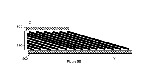
In Figure 5E, the substrate 500 is overlaid onto the previously placed HTS
tapes 510, at
most up to the starting point for the next HTS tape to be laid. (it should be
noted that this
figure is a linear representation of an HTS coil, so the point X on the
substrate shown
overlaying the HIS tapes may be the same as the point Y on the substrate
underlying
the HIS tapes further down the figure). By continually laying down additional
substrate
and further HIS tapes, the HIS coil can be built up to any desired number of
turns.
The result of the winding method shown in Figure 5 is an HTS field coil
comprising a
plurality of HIS tapes arranged to form turns, and a substrate separating each
of the
turns. The turns form a coiled path around the inner perimeter of the field
coil, where the
distance from that inner perimeter increases monotonically with movement in a
first
direction along the coiled path. For each HIS tape except the innermost tape,
each end
of the HTS tape is offset in the first direction from the corresponding end of
an adjacent
HTS tape which is radially inward of the HTS tape, and the HTS tape overlaps
the
adjacent HTS tape by at least 50% of its length. A 50% overlap would provide a
coil
having only two tapes in any given cross section of a turn, so in coils with
significant
current requirements the overlap may be at least 90% (10 tapes per turn cross
section)
or at least 95% (20 tapes per turn cross section). Each HTS tape has a length
less than
a perimeter of the coil plus the magnitude of the offset to the next tape
(i.e. the adjacent
tape which is radially outward). This is the maximum length which allows the
next tape
CA 03237540 2024- 5-7
WO 2023/083956
PCT/EP2022/081459
9
to be placed in a position where the substrate has not yet been laid down.
Particularly
for coils with a high degree of overlap, i.e. where the overlaps are short and
on the order
of the minimum bending radius of the substrate, the maximum length may be
considered
as the perimeter of the coil.
Figure 6 shows how grading of the coil can be achieved by varying the
distances Sn En
that the HIS tapes 610 overlap each other. In region 601 the offset distances
are such
that there are 3 HTS tapes in a cross section of the coil. In region 602, the
offset
distances are increased, and the coil grades down to only have two HTS tapes
in a given
cross section. In region 602, the offset distances are reduced, and the coil
grades up to
having 5 HTS tapes in a given cross section. In general, in areas of the coil
where those
distances are larger, the number of HIS tapes within a given cross section of
the cable
will decrease, and where those distances are smaller the number of HIS tapes
in a given
cross section of the cable will increase. As the zero-field critical current
at a given
temperature is dependent on the amount of HIS conductor in a cross section of
a turn,
this will result in grading of the coil. In general the offset distances may
vary around the
coil, and in a particular example they may vary such that the average offset
is greater in
a first arc of the coil (reducing the current density in that arc) than in a
second arc of the
coil (increasing the current density in that arc), for all turns of the coil
(i.e. such that the
grading of a given arc is similar for all turns).
Depending on the required properties of the final coil, the substrate may be
an insulator,
a conductive material connecting the turns, a semiconductor, or any
combination thereof
(e.g. an insulating strip having conductive paths running through it to
radially connect the
turns with a predetermined resistance). The substrate may comprise a
conductive
material having a channel within it, and the HIS tape may be laid within that
channel, in
which case the substrate may additional comprise an insulating layer on the
outside of
the conductive material to separate the turns, which may or may not have
conductive
paths through it.
Current flowing through the coil will need to move between HIS tapes as each
tape
ends. The substantial overlap between tapes means that the resistance
introduced by
this is very low, and any minor increase in Joule losses can be compensated
for by
additional cooling of the HTS coil by methods well known in the art. The tapes
are fixed
by a conductive fixing medium (e.g. solder or a conductive resin such as a
conductive
CA 03237540 2024- 5-7
WO 2023/083956
PCT/EP2022/081459
epoxy resin, or a resin impregnated with conductive material), and most of the
current
transfer between tapes will happen within this medium and within the
conductive (e.g.
copper) cladding on the individual tapes. Further improvements to the
resistance may
be obtained by providing an additional conductive path which bridges the sides
of all
5 tapes, meaning that current flowing from the "bottom" of the tape stack
to the "top" of the
tape stack only needs to travel through that conductive path, rather than
through each
intermediate HIS tape. This conductive path may be provided by a separately
bonded
conductive element, or, as shown in Figure 7 which is an end-on cross-section
of a turn
of the coil, the substrate may comprise a u-shaped copper channel 701 into
which the
10 HTS tapes 702 are laid, where the sides of the u-shape will form the
conductive path.
The substrate may comprise additional elements 703, 704 to separate the turns
and/or
insulate the outer edges of the u-shaped channel.
The HTS tapes may be fixed into place by impregnating the coil with solder or
other fixing
medium (e.g. conductive resin) after winding. Alternatively, solder or other
fixing medium
may be co-wound with the HIS tapes and melted, cured, or otherwise induced to
fix the
tapes during winding. The latter process reduces the time HTS material spends
at
elevated temperature and also allows the bonding of each HIS tape to be
monitored for
defects during winding, allowing any mistakes to be detected and potentially
corrected
(e.g. by reflowing solder, or reversing the bond and rewinding that section of
tape) during
the winding process.
Figure 8 shows an exemplary apparatus for laying HTS tapes for the above
winding
method. The apparatus follows the path of the coil (comprising the substrate
850 and
already laid HTS tapes 851), and has guides 801 which maintain its alignment
to the coil.
The apparatus has an HTS tape spool 802 containing HTS tape 803, which is laid
out
onto the coil as the apparatus travels in a first direction (right in the
figure, hereafter "up
the coil" though this should be recognised as a relative direction only), fed
out from the
spool 802 by a feeding mechanism which comprises an extruder 804 and/or a
motor
configured to turn the HIS tape spool, and a roller 805 or other similar means
which may
be spring loaded or similarly biased to press the HTS tape against the already
laid tapes
of the coil (or the substrate). A bonding agent, e.g. solder paste, a resin
such as an
epoxy resin, conductive epoxy, or solder flux, is applied via a nozzle or
other dispenser
806, located up the coil from roller, such that the deposited bonding agent
ends up
between the HTS tape 803 and the already laid HTS tapes 851. A bonding agent
CA 03237540 2024- 5-7
WO 2023/083956
PCT/EP2022/081459
11
activator 807 is present (if required) down the coil from the roller, to
provide any heating,
curing, or other activation required for the bonding agent ¨for example the
bonding agent
activator may be a heater which provides heating to a temperature sufficient
to melt
solder. Sensors 808 may be used down the coil from the roller, e.g. either
side of the
bonding agent activator, to measure whether the bond between the HTS tape 803
and
the already laid HIS tapes 851 is acceptable. These sensors may include
cameras,
electrical sensors, heat sensors (e.g. thermal cameras or temperature probes)
or any
other suitable sensor. Determination of whether the bond is acceptable may be
based
on pre-calibrated values, determination via machine learning based on known
good and
known bad samples, or human monitoring of sensor outputs or a sample thereof.
The apparatus includes a tape cutter 809, e.g. a knife, located up the coil
from the roller,
which cuts the tape when the apparatus reaches the location where a given tape
should
end.
During laying of the tape, the apparatus lays each HTS tape starting from a
first end, and
continues travelling up the coil and laying the tape until it reaches the
desired end point
of the tape, at which point the tape is cut and the apparatus continues
travelling without
feeding out additional tape until the HTS tape is bonded to the previously
laid HIS tape
all the way to the end. The apparatus then moves back down the coil to the
starting point
for the next HTS tape, and repeats the process. In this way, the apparatus can
lay
several HTS tapes along the coil as described with reference to Figure 5A to
E.
A position sensor 810 may be used to monitor the amount of tape dispensed from
the
HTS tape spool 801, and to determine whether there is sufficient tape
remaining to
dispense the next HIS tape onto the coil. A further position sensor 811 may be
used to
determine where on the coil the apparatus is located and so determine when to
start and
end laying of an HTS tape according to a preconfigured laying pattern for the
desired
coil.
In effect, the apparatus "rides" over the coil like the cart on a roller-
coaster travelling back
and forth with tape being laid when it is travelling "up" the coil, then the
tape is cut, and
then the apparatus travels "down" the coil to the starting point for the next
tape. The
apparatus may include a propulsion system such as powered wheels, or having
the
guides alternately grip the coil or support structures thereof and move
relative to the
CA 03237540 2024- 5-7
WO 2023/083956
PCT/EP2022/081459
12
apparatus so that it can "crawl" along the coil. Alternatively, the propulsion
system may
be external to the main apparatus, e.g. a gantry configured to move the
apparatus
appropriately around the coil.
The operation of the apparatus is controlled by a controller, which may be
integral with
the apparatus or may be a remote device which sends appropriate inputs to the
apparatus. The controller causes the various components of the apparatus to
perform
the tape laying method as described above. In some implementations the
controller may
be distributed through several components, e.g. as a distributed computing
architecture,
or as individual electrical or mechanical control systems for individual
parts, which may
be coordinated by a central controller.
To ensure that the start of an HTS tape is properly bonded to the coil, the
apparatus may
move to deposit a patch of bonding agent at the start location of the HTS
tape, and then
dispense HTS tape onto that patch of bonding agent to form an initial strong
bond before
continuing to dispense tape.
The apparatus shown above will lay the HTS tape according to the example of
Figures
5A to E, but does not lay the substrate itself. As shown in Figure 9, this may
be done by
a separate spool 901 which travels around the coil 902 continuously, e.g. at
the average
speed of the HTS tape laying apparatus, so that there is always substrate 910
for the
HTS tape to be laid onto at the end of an HTS tape length (where it does not
overlay any
previous tape), but also so that the substrate is not laid on top of the
starting location of
a not yet laid tape. The apparatus 903 of figure 8 then follows this spool,
moving back
and forth to lay individual HTS tapes.
An alternative "hybrid" winding method is shown schematically in Figure 10.
This method
combines features of the conventional winding method shown in Figure 2 or 3,
and the
novel winding method shown in Figure 5A-E, and may be advantageous, for
example, in
situations where the additional resistance introduced by the winding method of
Figure
5A-E is unacceptable. In the hybrid winding method, the coil is wound
initially according
to the conventional method shown in Figure 2 or 3, or any other continuous
winding
method in which an HTS cable is wound to form a field coil. During this
winding method
¨ either simultaneously with winding the HTS cable, or during a pause in the
winding of
the HTS cable¨ the winding method shown in Figure 5A-E is used to lay down a
plurality
CA 03237540 2024- 5-7
WO 2023/083956
PCT/EP2022/081459
13
of layers of tape in electrical contact with the HTS cable, along an arc of
the field coil.
These plurality of layers of tape will act as a "shunt" for the HTS cable,
which is in
electrical contact with the cable and can share current with the HTS cable,
thus providing
additional current paths (and hence additional current carrying capacity)
along the arc of
the field coil.
The shunt functions in a similar manner to those described in European Patent
EP
3747034 B1 , except that instead of a single HTS tape or conventional stack of
HTS
tapes, the HTS shunt has the arrangement of overlapping tapes discussed above,
i.e.
where the start and end of each HTS tape of the shunt is offset in one
direction around
the coil from the start and end of the HTS tape radially inward of it. Similar
modifications
may be made to the tapes of the HTS shunt as discussed above for a coil wound
entirely
using the method of Figure 5 ¨ e.g. the spacing of the HTS tapes of the HTS
shunt may
be varied to control the amount of HTS in any given cross section of the field
coil, or an
additional conductive path may be provided on the side of the HTS shunt, or
any other
modification previously discussed.
In the example of Figure 10, a spool 1001 of HIS cable 1010 is used to provide
the main
winding 1011 in a manner analogous to the spool 201 and HTS cable 210 of
Figure 2.
An apparatus 1003 according to figure 8 and the associated description travels
along the
main winding, and lays down additional HTS tape 1020 in a selected region 1021
(in the
example shown, in the central column section of a toroidal field coil) to form
the HIS
shunt. The apparatus 1003 may follow the main winding spool 201 around the
coil (i.e.
travelling around the coil outside of the region 1021 but not laying
additional tape), or
may be removed from the coil when cable is being wound from the main winding
spool,
and reintroduced whenever a section of additional HTS tape is to be laid down.
A
plurality of HTS shunts may be added around the coil, and HIS shunts may be
added to
any number of the turns of the main winding.
Figure 11 schematically illustrates a close up of a single turn in a region
having additional
tape, following winding of the coil. The turn comprises the HTS cable forming
the field
coil 1101 (of which only a section is shown). In the arc 1110, an HTS shunt
comprising
HIS tapes 1111 is provided on the HIS cable. While only four HIS tapes are
shown in
the figure, any number of HIS tapes may be used to form the HTS shunt,
provided that
for each HTS tape other than the radially inner HTS tape, each end of the HTS
tape is
CA 03237540 2024- 5-7
WO 2023/083956
PCT/EP2022/081459
14
offset in the first direction from the corresponding end of an adjacent HIS
tape which is
radially inward of the said HTS tape.
There will be some resistance between the main HTS coil and the HTS shunts,
but this
will be very low as current can transfer to or from the shunts along their
whole length.
This is also true if the coil is provided without insulation, such that
current can enter the
shunts from either side ¨ though where the HIS shunt is made from HIS tapes
having
substrates, the resistance on the substrate side of the HTS shunt would be
higher than
that on the HIS side. As such, when the current in the coil is such that if
the critical
current of the main HIS cable alone is not sufficient in the arc with the
shunts to carry
the transport current, then excess current will be easily shared to the HIS
shunts_ At
currents less than the critical current of the main HIS cable in the graded
region, the
vast majority of the current will primarily flow in the main HIS cable. As the
HIS cable
current approaches the critical current of the parts of the cable experiencing
higher
magnetic field (or higher temperature, or magnetic field angle less well
aligned with the
c-axis of the ReBCO HTS layer), the HIS will generate a voltage which will
drive excess
current through the small resistance between the main cable and the shunt. The
voltage
n
generated per metre of HIS (EHTs) is given by E
¨HTS = E0 (-)where Eo= 1 pV/cm is the
defined critical current criterion, /c is the critical current of the tape at
this criterion, and
n is an experimental parameter that models the sharpness of the
superconducting to
normal transition; n is typically in the range 20-50 for ReBCO. Depending on
the value
of n, the voltage is negligible for values of a = I/Ic less than about 0.8.
The excess current
above the local critical current will be shared into the shunt. This will
happen with minimal
dissipation, and the small amount of heat generated will be accommodated by
the design
of the coil cooling system. The number of shunts, and the number of tapes in
each shunt,
may be chosen based on the amount of HTS needed to keep the ratio a
approximately
the same in all parts of the coil. The main HIS cable may have any structure
which
permits the HIS shunt to be electrically connected to it, for example it may
be a stacked
tape cable.
Where shunts are provided along an arc of the coil, they may be provided
evenly to all
turns of the HIS cable (e.g. each turn of the HIS cable may have an HIS shunt
comprising two tapes), or the distribution of the shunts may vary across the
coil cross
section (e.g. providing shunts to every turn towards the outside of the
central column for
a IF coil, and providing shunts only to every other turn and/or shunts with
fewer HIS
CA 03237540 2024- 5-7
WO 2023/083956
PCT/EP2022/081459
tapes for turns towards the inside of the central column of a TF coil, as the
magnetic field
is lower).
While the above example has considered a situation where the HTS shunt is laid
down
5 by a method similar to that shown in Figure 5A-E, the apparatus of figure
8 could also be
used to lay down an HTS shunt as a more typical stacked tape cable. For
example,
where each tape overlies a portion of the previously laid down tape (i.e. with
each tape
being laid down with each end offset towards the centre of the tape relative
to the
previously laid tape), or where each tape completely overlies the previously
laid down
10 tape, or any other arrangement which can be formed by sequentially
laying down HIS
tapes.
CA 03237540 2024- 5-7