Note: Descriptions are shown in the official language in which they were submitted.
- 1 - OE00164R
CIRCUIT BOARD SPACING AND SUPPORT APPARATUS
Fi~ld of tl~ Inv~ntion
This invention relates generally to the electronic
assembly field and particularly to the circuit board ~pacer and
support field.
15 Backezound of th~ In~iQ~
When more than one printed circuit board is installed
in a device, they may be mounted one above the other to reduce
the amount of space required. Spacing supporters are
2 0 typically used to separate the boards for better cooling air flow
and to reduce the risk of contact of circuits on the separate
boards.
Spacing ~upporters are manufactured in various
shapes and sizes depending an the application. The distance
2 5 required between boards typically determines the length of the
spacing supporter. The board's density typically determines
the type of spacing supporter required.
Spacing supporters can be of two types: one type i8
inserted in a hole in the board and another is attached to the
3 0 edge of the board. A spacing supporter that i8 inserted in a
hole in the board cannot be used with a dense board since the
hole takes up valuable room. In this situation, a spacing
supporter that attaches to the side of the board is typically
used.
3 5 A problem with edge of board supporters is that the
opening in the support that retains the circuit board is
:- . . : - - ~ ;,
~"
- 2 - CE00164R
typically sized 90 a~ to accept a board in it~ worst case thickest
condit;on. This mean~ that acceptable boards that are even
slightly thinner can rattle and move about. This is
unacceptable with respect to vibration, audible noise, and
movement induced circuit noise.
Both type~ of spacing supporters have the common
problem of being comple~ly shaped. The complex designs
require expensive tooling to manufacture the spacing
supporters. This in tu~ leads to more expensive spacing
1 0 supporters. There is a resulting need for a less costly printed
circuit board spacing supporter that can be used with dense
boards and that retains the circuit board rigidly without
requiring additional elements.
1 S ~mmarv of ~h~
The present invention separates and rigidly supports
printed circuit boards. This apparatus is manufactured as a
single, rectangularly shaped strip of material Each end of the
2 0 strip contains a notch on the same side. On the opposite side
of and immediately behind the notches, are shallow
indentations. The width of the apparatus from the end of each
indentation to each end of the apparatus i8 less than the w~dth
of the mit-section af the apparatus.
2 5 The dimensions of the spacing supporter apparatus are
dependent on the application. A longer apparatus and a
greater distance between notches is required for an
application requiring a greater distance between circuit
boards. The dimensions of the notches are dependent on the
3 0 thickness of the circuit boards.
The notches are positioned on the edges of the circuit
boards to be separated, the upper notch of the apparatus is
attached to the upper board and the lower notch to the lower
board. The smaller width of the apparatus at the point of the
3 5 notch and indentation allows that part to flex around the
. . . .
:
.~ ' ; ' .
. '
.
- 3 - CE00164R
board~ holding it tightly as compared to current non-flexing
notche~.
Brief De~d~Q~ the I~ vin~
,~, 5
y FIG. 1 show the present invention in a typical application;
FIG. 2 shows a close up of one end of the pre~ent invention;
, and
~ FIG. 3 shows a close up of one end of the present invention
;~ l 0 indicating various angles.
FIG. 4 shows the present invention used with a worst case
thickness circuit board.
Be~ Mode fo~ C~e Out the Invent~
:; 1 5
The present invention separates and rigidly supports
printed circuit boards installed within an electronic device.
The apparatus, the preferred embodiment illustrated in Fig.
1, can function using minimal board space. In addition, due
2 0 to the simplicity of design, it can be manufactured relatively
inexpensively.
The apparatus i8 manufactured from a single piece of
material, the preferret embotiment being plastic. The
material used must be resilient, allowing the apparatus to flex
2 5 without breaking and to return to its original shape after use.
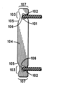
The apparatus includes notches (101) on the same side
at each end. The center of each notch (101) is located
approsimately .090 inches from the end. The width of the
notch (101) opening, .057 i .002 inches in the preferred
3 0 embodiment, accommodates a stantard width printed circuit
board. The sides of the notches (101) that face each other are
angled outward by approximately 15 a~ illustrated in Fig. 3.
This creates an opening of each of the notches (101) that is
narrower than the rest of the notch (101).
3 5 At each end on the opposite side of the apparatus,
im nediately behind each notch (101), is an indentation (103).
. .,. ~
- . .
, .
.. . . .
. . .
- 4 - CE00164R
These shallow indentations (103) are .030 inches deep as
measured from the mid-section (104) of the apparatus. The
initial ~lope (105) ofthe indentation (103) is approximately 30
from the mid-section (104) as illustrated in Fig. 3. These
S intentations (103) may be flat as shown in Fig. 1 or form a
radiu~ a~ shown in Fig. 3. The indentation (103), in
conjunction with the notch (101), creates a narrow, flexible
section (106) at each end of the apparatus.
The end section (107) of the apparatus after the
l O indentation is a narrower width than the mid-section (104).
The width of the mid-~ection (104) i~ approximately .130 inches
while the end sections (107) are approximately .115 inches.
The circuit board spacing and support apparatus
operates, as illustrated in Fig. 1 and Fig. 2, by inserting a
15 board in each notch (101). For correct operation, the opening
of the notch (101) should be narrower than the thicknes~ of the
circuit board. The narrow, flexible region (106) created by the
combination of a notch (101) and an indentation (103) fle~ces,
allowing the thicker board to be inserted. Once the board is
2 0 inserted, the flexible part, attempting to return to its original
shape, will force the upper part of the notch (102) to put
pressure on the board. This pressure will hold the board in
place against the lower part of the notch. Due to the small
area that is in contact ~qith the board, minimal board space is
2 S required to hold the board solidly.
Fig. 4 illustrates the present invention used ~nth a
circuit board having a worst case thickness. The narrower
end of the apparatus can fle~c back without protruding past the
oubide surface of the apparatus. This allows the apparatus to
3 0 be used with thicker boards without requiring additional
space.
The dimensions and material of this apparatus will
vary depending on the application. The length of the
apparatus and the distance between the notches (101) will vary
3 5 depending on the distance required between the boards. The
thickness of the apparatus will vary depending on the
,
- 5 - CE00164R
~ 3 ~-9
strength required. The apparatus's composition msy be a
; high temperature material when the environment has a high
ambient temperature.
l~e printed circuit board spacing and support
S apparatus di~closed above is relatively ine~pensive to
manufacture due to its ~imple de~ign. An additional benefit is
that very little board space i8 required since holes in the board
are not needed and the apparatus rigidly grips the board with
a small surface area.
10Those skilled in the art vill recognize that various
modifications and changes could be made to the invention
~vithout departing from the spirit and scope thereof. It should
therefore be understood that the claims are not to be
considered as being limited to the precise embodiments set
l S forth in the absence of specific limitations directed to such
embodiments.
.. ~' - . ': .
, .