Language selection

Search

Patent 2073392 Summary

Third-party information liability

Some of the information on this Web page has been provided by external sources. The Government of Canada is not responsible for the accuracy, reliability or currency of the information supplied by external sources. Users wishing to rely upon this information should consult directly with the source of the information. Content provided by external sources is not subject to official languages, privacy and accessibility requirements.

Claims and Abstract availability

Any discrepancies in the text and image of the Claims and Abstract are due to differing posting times. Text of the Claims and Abstract are posted:

  • At the time the application is open to public inspection;
  • At the time of issue of the patent (grant).
(12) Patent: (11) CA 2073392
(54) English Title: PARABOLIC SIGNAL GENERATOR
(54) French Title: GENERATEUR DE SIGNAUX PARABOLIQUE
Status: Deemed expired
Bibliographic Data
(51) International Patent Classification (IPC):
  • G09G 1/04 (2006.01)
  • H03K 4/04 (2006.01)
  • H04N 3/16 (2006.01)
(72) Inventors :
  • YAMATE, KAZUNORI (Japan)
(73) Owners :
  • MATSUSHITA ELECTRIC INDUSTRIAL CO., LTD. (Not Available)
(71) Applicants :
(74) Agent: MARKS & CLERK
(74) Associate agent:
(45) Issued: 1998-07-21
(22) Filed Date: 1992-07-08
(41) Open to Public Inspection: 1993-01-13
Examination requested: 1992-07-08
Availability of licence: N/A
(25) Language of filing: English

Patent Cooperation Treaty (PCT): No

(30) Application Priority Data:
Application No. Country/Territory Date
03-172537 Japan 1991-07-12

Abstracts

English Abstract


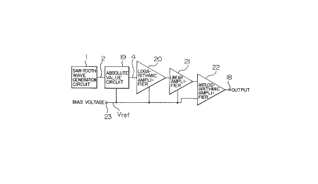
In a parabolic signal generator, a sync pulse
is applied to a saw-tooth wave generation circuit, the
output of the saw-tooth wave generation circuit is
entered to an absolute value circuit, the output of the
absolute value circuit is entered to a logarithmic
amplifier, the output of the logarithmic amplifier is
entered to a linear amplifier, and the output of the
linear amplifier is entered to an antilogarithmic
amplifier. The absolute value circuit, logarithmic
amplifier, linear amplifier and antilogarithmic
amplifier are powered by a single-voltage power source,
and these circuit and appliers have reference input
terminals supplied with a common bias voltage.


French Abstract

Dans un générateur de signal parabolique, une impulsion de synchronisation est appliquée à un circuit générateur d'ondes en dents de scie, dont la sortie est transmise à un circuit à valeur absolue. La sortie de ce dernier est transmise à un amplificateur logarithmique, dont la sortie est transmise à un amplificateur linéaire. La sortie de l'amplificateur linéaire est transmise à un amplificateur antilogarithmique. Le circuit à valeur absolue, l'amplificateur logarithmique, l'amplificateur linéaire et l'amplificateur antilogarithmique sont alimentés par une source à tension simple, et ils ont des bornes d'entrée de référence soumises à une tension de polarisation commune.

Claims

Note: Claims are shown in the official language in which they were submitted.


THE EMBODIMENTS OF THE INVENTION IN WHICH AN EXCLUSIVE PROPERTY
OR PRIVILEGE IS CLAIMED ARE DEVINED AS FOLLOWS:


1. A parabolic signal generator in which a sync
pulse is applied to a saw-tooth wave generation circuit,
the output of said saw-tooth wave generation circuit is
entered to an absolute value circuit, the output of said
absolute value circuit is entered to a logarithmic
amplifier, the output of said logarithmic amplifier is
entered to a linear amplifier, and the output of said
linear amplifier is entered to an antilogarithmic
amplifier.
2. A parabolic signal generator according to
claim 1, wherein said absolute value circuit, logarithmic
amplifier, linear amplifier and antilogarithmic
amplifier are powered by a single-voltage power source,
and said absolute value circuit, logarithmic amplifier,
linear amplifier and antilogarithmic amplifier have
reference input terminals supplied with a common bias
voltage.


Description

Note: Descriptions are shown in the official language in which they were submitted.


~733~


1 BACKGROUND OF THE INVENTION
This invention relates to a parabolic signal
generator used with the deflection circuit and dynamic
focusing circuit (will be termed "DAF" hereinafter) of
television receivers and display apparatus.
In order to improve the focus characteristics
of the cathode ray tube (will be termed "CRT" herein-
after) used in recent television receivers and display
apparatus having large screens, DAF circuits are intro-

duced so as to improve the peripheral focus character-
istics of the CRT. This purpose is achieved by operat-
ing the DAF circuit to generate a parabolic waveform and
applying the waveform to the focus terminal of the CRT.
The following explains a conventional
parabolic signal generator. Fig. 2 shows the
conventional parabolic signal generator. In Fig. 2,
symbol 1 denotes a saw-tooth wave generation circuit, 3
is an absolute value circuit, 5, 7, 10, 14, 17 and 24
are resistors, and 6, 8, 9, 11, 12, 13, 15 and 16 are
20 diodes.
The operation of the foregoing conventional
circuit arrangement will be explained. The saw-tooth
wave generation circuit 1 converts a current flowing in
the deflection coil into a voltage shown in Fig. 3A, the
25 absolute value circuit 3 folds the saw-tooth waveform


2~73:3~2

., ~ .
1 with respect to its center to produce a waveform shown
in Fig. 3B, and a polygonal approximation circuit formed
of the resistors 5, 7, 10, 14, 17 and 24 and the diodes
6, 8, 9, 11, 12, 13, 15 and 16 operates to make parallel
connections of registers in response to the conduction
of sets of diodes which are in serial connection with
the respective resistors, so that a parabolic waveform
is produced.


SUMMARY OF THE INVENTION
However, in the foregoing conventional
arrangement based on the characteristics of diode, the
parabolic waveform fluctuates due to the thermal
characteristics of the diodes, and in addition the
number of resistors and diodes must be changed for
changing the waveform parameter of the parabolic wave
(generally, a parabolic waveform is defined for the
input X and output Y as:

Y = X~ ~.- (1)

where ~ is a real number) when the focus characteristics
of CRT is altered or the CRT screen size is altered.
The present invention is intended to solve the
foregoing prior art deficiency, and its object is to
provide a parabolic signal generator which realizes the
expression (1) by means of a logarithmic amplifier, a
linear amplifier and an antilogarithmic amplifier. The

20~3~-

1 logarithmic amplifier needs to have an input voltage
which is higher than its reference voltage because of
the definition of logarithm in the range of positive
real numbers, and on this account the absolute value
circuit which precedes the logarithmic amplifier has its
reference voltage made equal to that of the logarithmic
amplifier so that the input of the logarithmic amplifier
does not fall undefined.
In order to achieve the above objective, the
inventive parabolic signal generator is designed to
apply a sync pulse to a saw-tooth wave generation
circuit, enter the output of the saw-tooth wave gener-
ation circuit to an absolute value circuit, enter the
output of the absolute value circuit to a logarithmic
amplifier, enter the output of the logarithmic amplifier
to a linear amplifier, and enter the output of the
linear amplifier to an antilogarithmic amplifier. The
absolute value circuit, logarithmic amplifier, linear
amplifier and antilogarithmic amplifier are powered by a
single-voltage power source, and these circuit and
amplifiers have their reference input terminals supplied
with a common bias voltage.
Based on the foregoing arrangement, the
parameter a of the expression (1) can be determined by
setting the gain of the linear amplifier (generally, it
is given as a ratio of resistances of two resistors),
and when the ~ is determined as characteristics of CRT,
the gain of the linear amplifier is simply set to ~, and


1 the input voltage to the logarithmic amplifier is
guarantied to be higher than the reference voltage of
the logarithmic amplifier.


BRIEF DESCRIPTION OF THE DRAWINGS
Fig. 1 is a block diagram of the parabolic
signal generator based on an embodiment of this
invention;
Fig. 2 is a schematic diagram of the con-
ventional parabolic signal generator;
Fig. 3A is a waveform diagram of the saw-tooth
wave signal; and
Fig. 3B is a waveform diagram of the output
signal of the absolute value circuit.


DESCRIPTION OF THE PREFERRED EMBODIMENT
An embodiment of this invention will be
described with reference to the drawings. In Fig. 1,
symbol 1 denotes a saw-tooth wave generation circuit, 2
is a saw-tooth wave signal, 19 is an absolute value
circuit which receives the saw-tooth wave signal, 4 is
an output signal of the absolute value circuit, 20 is a
linear amplifier which receives the output of the
absolute value circuit, 21 is a linear amplifier which
receives the output of the logarithmic amplifier, 22 is
an antilogarithmic amplifier which receives the output
of the linear amplifier, 23 is a reference voltage input
terminal, and 18 is an output terminal for the output


9~

1 which is expressed as Y in the expression (1) (in which
denotes the gain of the linear amplifier 21).
The operation of the parabolic signal
generator arranged as described above will be explained
5 on Figs. 3A and 3B.
The saw-tooth wave signal 2 shown in Fig. 3A
is applied to the absolute value circuit 19, which then
produces the output signal 4 shown in Fig. 3B. The
reference voltage Vref is set to the level which crosses
10 the center of the saw-tooth wave signal 2 as shown in
Fig. 3A. Accordingly, point A in Figs. 3A and 3B does
not fall below the reference voltage Vref, and thus it
does not become an undefined voltage for the logarithmic
amplifier 20 located in the following stage.
The expression (1) is realized by the
operations of the logarithmic amplifier 20, linear
amplifier 21 and antilogarithmic amplifier 22 as
follows.
The output Yl of the logarithmic amplifier 20,
20 the output Ya of the linear amplifier 21, and the output
Y0 of the antilogarithmic amplifier 22 are given as
functions of the input voltage X as follows.


Yl = log X ... (2)


Ya = ~ log X = log X ... (3)


Y0 = log X-l(log X~) = X~ ... (4)

2Q73~
1 According to this invention, as described
above, the logarithmic amplifier does not have undefined
regions through the provision of a common reference
voltage for the absolute value circuit, logarithmic
amplifier, linear amplifier and antilogarithmic
amplifier. Moreover, the parameter ~ of the expression
(1) can be altered by setting the gain of the linear
amplifier arbitrarily, whereby the signal generator can
readily be modified when the CRT is switched to another
type. The operation expressed by the expressions (1),
(2), (3) and (4) produces accurate parabolic waveforms.
Consequently, the parabolic waveform signal generator
based on this invention can be designed efficiently, the
circuit arrangement shown in Fig. 1 is suitable for
circuit integration for cost reduction, and the
influence of the thermal characteristics of diode on the
waveform, which is encountered in the prior art circuit
arrangement, can be eliminated according to this
invention.


Representative Drawing
A single figure which represents the drawing illustrating the invention.
Administrative Status

For a clearer understanding of the status of the application/patent presented on this page, the site Disclaimer , as well as the definitions for Patent , Administrative Status , Maintenance Fee  and Payment History  should be consulted.

Administrative Status

Title Date
Forecasted Issue Date 1998-07-21
(22) Filed 1992-07-08
Examination Requested 1992-07-08
(41) Open to Public Inspection 1993-01-13
(45) Issued 1998-07-21
Deemed Expired 2009-07-08

Abandonment History

There is no abandonment history.

Payment History

Fee Type Anniversary Year Due Date Amount Paid Paid Date
Application Fee $0.00 1992-07-08
Registration of a document - section 124 $0.00 1993-02-19
Maintenance Fee - Application - New Act 2 1994-07-08 $100.00 1994-05-05
Maintenance Fee - Application - New Act 3 1995-07-10 $100.00 1995-05-30
Maintenance Fee - Application - New Act 4 1996-07-08 $100.00 1996-05-09
Maintenance Fee - Application - New Act 5 1997-07-08 $150.00 1997-05-22
Final Fee $300.00 1998-03-30
Maintenance Fee - Application - New Act 6 1998-07-08 $150.00 1998-05-19
Maintenance Fee - Patent - New Act 7 1999-07-08 $150.00 1999-06-11
Maintenance Fee - Patent - New Act 8 2000-07-10 $150.00 2000-06-19
Maintenance Fee - Patent - New Act 9 2001-07-09 $150.00 2001-06-18
Maintenance Fee - Patent - New Act 10 2002-07-08 $200.00 2002-06-17
Maintenance Fee - Patent - New Act 11 2003-07-08 $200.00 2003-06-19
Maintenance Fee - Patent - New Act 12 2004-07-08 $250.00 2004-06-16
Maintenance Fee - Patent - New Act 13 2005-07-08 $250.00 2005-06-07
Maintenance Fee - Patent - New Act 14 2006-07-10 $250.00 2006-06-07
Maintenance Fee - Patent - New Act 15 2007-07-09 $450.00 2007-06-07
Owners on Record

Note: Records showing the ownership history in alphabetical order.

Current Owners on Record
MATSUSHITA ELECTRIC INDUSTRIAL CO., LTD.
Past Owners on Record
YAMATE, KAZUNORI
Past Owners that do not appear in the "Owners on Record" listing will appear in other documentation within the application.
Documents

To view selected files, please enter reCAPTCHA code :


To view images, click a link in the Document Description column. To download the documents, select one or more checkboxes in the first column and then click the "Download Selected in PDF format (Zip Archive)" or the "Download Selected as Single PDF" button.

List of published and non-published patent-specific documents on the CPD .

If you have any difficulty accessing content, you can call the Client Service Centre at 1-866-997-1936 or send them an e-mail at CIPO Client Service Centre.


Document
Description 
Date
(yyyy-mm-dd) 
Number of pages   Size of Image (KB) 
Representative Drawing 1998-07-13 1 5
Description 1993-12-15 6 204
Cover Page 1993-12-15 1 16
Abstract 1993-12-15 1 20
Drawings 1993-12-15 1 29
Description 1997-11-05 6 183
Claims 1993-12-15 1 27
Cover Page 1998-07-13 1 42
Description 1998-05-25 6 183
Description 1998-06-01 6 183
Correspondence 1998-03-30 1 40
Prosecution Correspondence 1993-12-10 1 19
Office Letter 1993-03-15 1 42
Fees 1997-05-22 1 67
Fees 1996-05-09 1 65
Fees 1995-05-30 1 61
Fees 1994-05-05 1 62