Sélection de la langue

Search

Sommaire du brevet 2073392 

Énoncé de désistement de responsabilité concernant l'information provenant de tiers

Une partie des informations de ce site Web a été fournie par des sources externes. Le gouvernement du Canada n'assume aucune responsabilité concernant la précision, l'actualité ou la fiabilité des informations fournies par les sources externes. Les utilisateurs qui désirent employer cette information devraient consulter directement la source des informations. Le contenu fourni par les sources externes n'est pas assujetti aux exigences sur les langues officielles, la protection des renseignements personnels et l'accessibilité.

Disponibilité de l'Abrégé et des Revendications

L'apparition de différences dans le texte et l'image des Revendications et de l'Abrégé dépend du moment auquel le document est publié. Les textes des Revendications et de l'Abrégé sont affichés :

  • lorsque la demande peut être examinée par le public;
  • lorsque le brevet est émis (délivrance).
(12) Brevet: (11) CA 2073392
(54) Titre français: GENERATEUR DE SIGNAUX PARABOLIQUE
(54) Titre anglais: PARABOLIC SIGNAL GENERATOR
Statut: Réputé périmé
Données bibliographiques
(51) Classification internationale des brevets (CIB):
  • G09G 1/04 (2006.01)
  • H03K 4/04 (2006.01)
  • H04N 3/16 (2006.01)
(72) Inventeurs :
  • YAMATE, KAZUNORI (Japon)
(73) Titulaires :
  • MATSUSHITA ELECTRIC INDUSTRIAL CO., LTD. (Non disponible)
(71) Demandeurs :
(74) Agent: MARKS & CLERK
(74) Co-agent:
(45) Délivré: 1998-07-21
(22) Date de dépôt: 1992-07-08
(41) Mise à la disponibilité du public: 1993-01-13
Requête d'examen: 1992-07-08
Licence disponible: S.O.
(25) Langue des documents déposés: Anglais

Traité de coopération en matière de brevets (PCT): Non

(30) Données de priorité de la demande:
Numéro de la demande Pays / territoire Date
03-172537 Japon 1991-07-12

Abrégés

Abrégé français

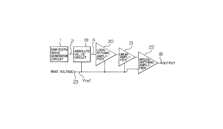
Dans un générateur de signal parabolique, une impulsion de synchronisation est appliquée à un circuit générateur d'ondes en dents de scie, dont la sortie est transmise à un circuit à valeur absolue. La sortie de ce dernier est transmise à un amplificateur logarithmique, dont la sortie est transmise à un amplificateur linéaire. La sortie de l'amplificateur linéaire est transmise à un amplificateur antilogarithmique. Le circuit à valeur absolue, l'amplificateur logarithmique, l'amplificateur linéaire et l'amplificateur antilogarithmique sont alimentés par une source à tension simple, et ils ont des bornes d'entrée de référence soumises à une tension de polarisation commune.


Abrégé anglais


In a parabolic signal generator, a sync pulse
is applied to a saw-tooth wave generation circuit, the
output of the saw-tooth wave generation circuit is
entered to an absolute value circuit, the output of the
absolute value circuit is entered to a logarithmic
amplifier, the output of the logarithmic amplifier is
entered to a linear amplifier, and the output of the
linear amplifier is entered to an antilogarithmic
amplifier. The absolute value circuit, logarithmic
amplifier, linear amplifier and antilogarithmic
amplifier are powered by a single-voltage power source,
and these circuit and appliers have reference input
terminals supplied with a common bias voltage.

Revendications

Note : Les revendications sont présentées dans la langue officielle dans laquelle elles ont été soumises.


THE EMBODIMENTS OF THE INVENTION IN WHICH AN EXCLUSIVE PROPERTY
OR PRIVILEGE IS CLAIMED ARE DEVINED AS FOLLOWS:


1. A parabolic signal generator in which a sync
pulse is applied to a saw-tooth wave generation circuit,
the output of said saw-tooth wave generation circuit is
entered to an absolute value circuit, the output of said
absolute value circuit is entered to a logarithmic
amplifier, the output of said logarithmic amplifier is
entered to a linear amplifier, and the output of said
linear amplifier is entered to an antilogarithmic
amplifier.
2. A parabolic signal generator according to
claim 1, wherein said absolute value circuit, logarithmic
amplifier, linear amplifier and antilogarithmic
amplifier are powered by a single-voltage power source,
and said absolute value circuit, logarithmic amplifier,
linear amplifier and antilogarithmic amplifier have
reference input terminals supplied with a common bias
voltage.


Description

Note : Les descriptions sont présentées dans la langue officielle dans laquelle elles ont été soumises.


~733~


1 BACKGROUND OF THE INVENTION
This invention relates to a parabolic signal
generator used with the deflection circuit and dynamic
focusing circuit (will be termed "DAF" hereinafter) of
television receivers and display apparatus.
In order to improve the focus characteristics
of the cathode ray tube (will be termed "CRT" herein-
after) used in recent television receivers and display
apparatus having large screens, DAF circuits are intro-

duced so as to improve the peripheral focus character-
istics of the CRT. This purpose is achieved by operat-
ing the DAF circuit to generate a parabolic waveform and
applying the waveform to the focus terminal of the CRT.
The following explains a conventional
parabolic signal generator. Fig. 2 shows the
conventional parabolic signal generator. In Fig. 2,
symbol 1 denotes a saw-tooth wave generation circuit, 3
is an absolute value circuit, 5, 7, 10, 14, 17 and 24
are resistors, and 6, 8, 9, 11, 12, 13, 15 and 16 are
20 diodes.
The operation of the foregoing conventional
circuit arrangement will be explained. The saw-tooth
wave generation circuit 1 converts a current flowing in
the deflection coil into a voltage shown in Fig. 3A, the
25 absolute value circuit 3 folds the saw-tooth waveform


2~73:3~2

., ~ .
1 with respect to its center to produce a waveform shown
in Fig. 3B, and a polygonal approximation circuit formed
of the resistors 5, 7, 10, 14, 17 and 24 and the diodes
6, 8, 9, 11, 12, 13, 15 and 16 operates to make parallel
connections of registers in response to the conduction
of sets of diodes which are in serial connection with
the respective resistors, so that a parabolic waveform
is produced.


SUMMARY OF THE INVENTION
However, in the foregoing conventional
arrangement based on the characteristics of diode, the
parabolic waveform fluctuates due to the thermal
characteristics of the diodes, and in addition the
number of resistors and diodes must be changed for
changing the waveform parameter of the parabolic wave
(generally, a parabolic waveform is defined for the
input X and output Y as:

Y = X~ ~.- (1)

where ~ is a real number) when the focus characteristics
of CRT is altered or the CRT screen size is altered.
The present invention is intended to solve the
foregoing prior art deficiency, and its object is to
provide a parabolic signal generator which realizes the
expression (1) by means of a logarithmic amplifier, a
linear amplifier and an antilogarithmic amplifier. The

20~3~-

1 logarithmic amplifier needs to have an input voltage
which is higher than its reference voltage because of
the definition of logarithm in the range of positive
real numbers, and on this account the absolute value
circuit which precedes the logarithmic amplifier has its
reference voltage made equal to that of the logarithmic
amplifier so that the input of the logarithmic amplifier
does not fall undefined.
In order to achieve the above objective, the
inventive parabolic signal generator is designed to
apply a sync pulse to a saw-tooth wave generation
circuit, enter the output of the saw-tooth wave gener-
ation circuit to an absolute value circuit, enter the
output of the absolute value circuit to a logarithmic
amplifier, enter the output of the logarithmic amplifier
to a linear amplifier, and enter the output of the
linear amplifier to an antilogarithmic amplifier. The
absolute value circuit, logarithmic amplifier, linear
amplifier and antilogarithmic amplifier are powered by a
single-voltage power source, and these circuit and
amplifiers have their reference input terminals supplied
with a common bias voltage.
Based on the foregoing arrangement, the
parameter a of the expression (1) can be determined by
setting the gain of the linear amplifier (generally, it
is given as a ratio of resistances of two resistors),
and when the ~ is determined as characteristics of CRT,
the gain of the linear amplifier is simply set to ~, and


1 the input voltage to the logarithmic amplifier is
guarantied to be higher than the reference voltage of
the logarithmic amplifier.


BRIEF DESCRIPTION OF THE DRAWINGS
Fig. 1 is a block diagram of the parabolic
signal generator based on an embodiment of this
invention;
Fig. 2 is a schematic diagram of the con-
ventional parabolic signal generator;
Fig. 3A is a waveform diagram of the saw-tooth
wave signal; and
Fig. 3B is a waveform diagram of the output
signal of the absolute value circuit.


DESCRIPTION OF THE PREFERRED EMBODIMENT
An embodiment of this invention will be
described with reference to the drawings. In Fig. 1,
symbol 1 denotes a saw-tooth wave generation circuit, 2
is a saw-tooth wave signal, 19 is an absolute value
circuit which receives the saw-tooth wave signal, 4 is
an output signal of the absolute value circuit, 20 is a
linear amplifier which receives the output of the
absolute value circuit, 21 is a linear amplifier which
receives the output of the logarithmic amplifier, 22 is
an antilogarithmic amplifier which receives the output
of the linear amplifier, 23 is a reference voltage input
terminal, and 18 is an output terminal for the output


9~

1 which is expressed as Y in the expression (1) (in which
denotes the gain of the linear amplifier 21).
The operation of the parabolic signal
generator arranged as described above will be explained
5 on Figs. 3A and 3B.
The saw-tooth wave signal 2 shown in Fig. 3A
is applied to the absolute value circuit 19, which then
produces the output signal 4 shown in Fig. 3B. The
reference voltage Vref is set to the level which crosses
10 the center of the saw-tooth wave signal 2 as shown in
Fig. 3A. Accordingly, point A in Figs. 3A and 3B does
not fall below the reference voltage Vref, and thus it
does not become an undefined voltage for the logarithmic
amplifier 20 located in the following stage.
The expression (1) is realized by the
operations of the logarithmic amplifier 20, linear
amplifier 21 and antilogarithmic amplifier 22 as
follows.
The output Yl of the logarithmic amplifier 20,
20 the output Ya of the linear amplifier 21, and the output
Y0 of the antilogarithmic amplifier 22 are given as
functions of the input voltage X as follows.


Yl = log X ... (2)


Ya = ~ log X = log X ... (3)


Y0 = log X-l(log X~) = X~ ... (4)

2Q73~
1 According to this invention, as described
above, the logarithmic amplifier does not have undefined
regions through the provision of a common reference
voltage for the absolute value circuit, logarithmic
amplifier, linear amplifier and antilogarithmic
amplifier. Moreover, the parameter ~ of the expression
(1) can be altered by setting the gain of the linear
amplifier arbitrarily, whereby the signal generator can
readily be modified when the CRT is switched to another
type. The operation expressed by the expressions (1),
(2), (3) and (4) produces accurate parabolic waveforms.
Consequently, the parabolic waveform signal generator
based on this invention can be designed efficiently, the
circuit arrangement shown in Fig. 1 is suitable for
circuit integration for cost reduction, and the
influence of the thermal characteristics of diode on the
waveform, which is encountered in the prior art circuit
arrangement, can be eliminated according to this
invention.


Dessin représentatif
Une figure unique qui représente un dessin illustrant l'invention.
États administratifs

Pour une meilleure compréhension de l'état de la demande ou brevet qui figure sur cette page, la rubrique Mise en garde , et les descriptions de Brevet , États administratifs , Taxes périodiques et Historique des paiements devraient être consultées.

États administratifs

Titre Date
Date de délivrance prévu 1998-07-21
(22) Dépôt 1992-07-08
Requête d'examen 1992-07-08
(41) Mise à la disponibilité du public 1993-01-13
(45) Délivré 1998-07-21
Réputé périmé 2009-07-08

Historique d'abandonnement

Il n'y a pas d'historique d'abandonnement

Historique des paiements

Type de taxes Anniversaire Échéance Montant payé Date payée
Le dépôt d'une demande de brevet 0,00 $ 1992-07-08
Enregistrement de documents 0,00 $ 1993-02-19
Taxe de maintien en état - Demande - nouvelle loi 2 1994-07-08 100,00 $ 1994-05-05
Taxe de maintien en état - Demande - nouvelle loi 3 1995-07-10 100,00 $ 1995-05-30
Taxe de maintien en état - Demande - nouvelle loi 4 1996-07-08 100,00 $ 1996-05-09
Taxe de maintien en état - Demande - nouvelle loi 5 1997-07-08 150,00 $ 1997-05-22
Taxe finale 300,00 $ 1998-03-30
Taxe de maintien en état - Demande - nouvelle loi 6 1998-07-08 150,00 $ 1998-05-19
Taxe de maintien en état - brevet - nouvelle loi 7 1999-07-08 150,00 $ 1999-06-11
Taxe de maintien en état - brevet - nouvelle loi 8 2000-07-10 150,00 $ 2000-06-19
Taxe de maintien en état - brevet - nouvelle loi 9 2001-07-09 150,00 $ 2001-06-18
Taxe de maintien en état - brevet - nouvelle loi 10 2002-07-08 200,00 $ 2002-06-17
Taxe de maintien en état - brevet - nouvelle loi 11 2003-07-08 200,00 $ 2003-06-19
Taxe de maintien en état - brevet - nouvelle loi 12 2004-07-08 250,00 $ 2004-06-16
Taxe de maintien en état - brevet - nouvelle loi 13 2005-07-08 250,00 $ 2005-06-07
Taxe de maintien en état - brevet - nouvelle loi 14 2006-07-10 250,00 $ 2006-06-07
Taxe de maintien en état - brevet - nouvelle loi 15 2007-07-09 450,00 $ 2007-06-07
Titulaires au dossier

Les titulaires actuels et antérieures au dossier sont affichés en ordre alphabétique.

Titulaires actuels au dossier
MATSUSHITA ELECTRIC INDUSTRIAL CO., LTD.
Titulaires antérieures au dossier
YAMATE, KAZUNORI
Les propriétaires antérieurs qui ne figurent pas dans la liste des « Propriétaires au dossier » apparaîtront dans d'autres documents au dossier.
Documents

Pour visionner les fichiers sélectionnés, entrer le code reCAPTCHA :


Pour visualiser une image, cliquer sur un lien dans la colonne description du document. Pour télécharger l'image (les images), cliquer l'une ou plusieurs cases à cocher dans la première colonne et ensuite cliquer sur le bouton "Télécharger sélection en format PDF (archive Zip)" ou le bouton "Télécharger sélection (en un fichier PDF fusionné)".

Liste des documents de brevet publiés et non publiés sur la BDBC .

Si vous avez des difficultés à accéder au contenu, veuillez communiquer avec le Centre de services à la clientèle au 1-866-997-1936, ou envoyer un courriel au Centre de service à la clientèle de l'OPIC.


Description du
Document 
Date
(yyyy-mm-dd) 
Nombre de pages   Taille de l'image (Ko) 
Dessins représentatifs 1998-07-13 1 5
Description 1993-12-15 6 204
Page couverture 1993-12-15 1 16
Abrégé 1993-12-15 1 20
Dessins 1993-12-15 1 29
Description 1997-11-05 6 183
Revendications 1993-12-15 1 27
Page couverture 1998-07-13 1 42
Description 1998-05-25 6 183
Description 1998-06-01 6 183
Correspondance 1998-03-30 1 40
Correspondance de la poursuite 1993-12-10 1 19
Lettre du bureau 1993-03-15 1 42
Taxes 1997-05-22 1 67
Taxes 1996-05-09 1 65
Taxes 1995-05-30 1 61
Taxes 1994-05-05 1 62