Note: Descriptions are shown in the official language in which they were submitted.
2~7728~
1 BACKGROUND OF THE INVENTION
The present inven~ion rPlates to a me~hod for
manufacturing a ROM type optical disk, and more
particularly to a method for obtaining application
S program data for writing in a ROM type optical disk
added with information on data writing positions showing
track and sector arrangement and the like in the
manufacture of -the ROM type optical disk~
There are those types of optical disks called
ROM and Partial-ROM (P-ROM). These are of such a type
that application program data are recorded in the whole
(ROM) or a part of (P-ROM) optical disk in advance, and
a general user can execute and mak~e access to the
application program data recorded on an optical disk
without writing the application program data in the
optical disk by oneself.
As the features of this ROM type optical disk,
such points may be mentioned that a sheet of stamper for
forming in which application program data are written is
manufactured and several thousand sheets of ROM type
optical disks are manufactured by resin molding using
this stamper, thereby enabling to supply ROM type
optical disks in which application program data are
written to a plurality of users at a low price.
-- 1 --
2~7728~
1 SU~MARY OF THE INVENTION
Here, in order to manufacture a stamper for
forming in which application pxogram data are written
while accommodating quickly, a supply configuration of
S data becomes a primary factor when the application
program data are supplied. As of now, however, the ROM
type optical disk is not on the market, and definite
techniques related to the supply configuration have
neither been established at present.
It is an object of the present invenkion to
convert application program data having no information
on positions for writing supplied data into application
program data having inforrnation on positions for writing
data easily and promptly.
Namely, according to the present invention,
there is provided a method for manufacturing a ROM type
optical disk with application program data written
therein, wherein application program data having no
information on positions for writing data stored in a
storage de~ice are written in an optical disk for
supplying data by a data writing optical disk drive, and
then application program data and information on
positions for writing data are read out of the optical
d~sk for ~upplying data by a data reading optical disk
drive and stored in a storage device for manufacturing a
ROM type optical disk.
The application program data having no
information on positions for writing the data stored in
2~7728~
1 the storage d~vice for supplying an application program
are written in an optical disk for supplying data using
an optical disk drive for writing data so as to show a
layout (track and sector axrangement) same as that of a
ROM type optical disk to be manufactured.
Next, th~ optical disk for supplying data in
which this application program data are writtPn is read
by means of an optical disk drive for reading the data
so as to store information on positions for writing the
data showing application program data, track and sector
arrangement and the like in the storage device for
manufacturing a ROM type optical disk.
The application program having writing
information stored in the storage unit ~or manufacturing
a RO~ type optical disk is modulated and recorded on a
glass original plate applied with photoresist by means
of a formatter and a cutting machine in accordance with
an established rule, a stamper is produced, resin
molding is performed with this sta~lper and a recording
layer and/or a reflective layer and ~he like are coated
thereon, thus manufacturing a ROM type optical disk.
Besides, the storage device may be any of
these that can execute input/output of data such as a
hard disk, an optical disk and a tape streamer.
Further, a write-once type or erasable type optical disk
is used for the disk for supplying the data. Since
rewriting of the data in the optical disk is possible
when an erasable type optical disk is used, it is
2~1772~
1 possible to use the same optical disk any number of
times for supplying the application program data.
BRIEF DESCRIPTION OF THE DRAWING
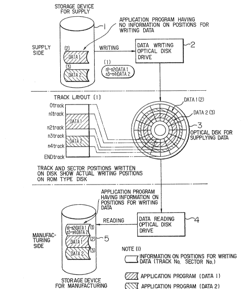
Fig. 1 is a diagram showing a flow of data
supply for manufacturing a ROM optical disk according to
the present invention.
DESCRIPTION OF PREFERRED EMBODIMENT
An embodiment of the present invention is
shown in Fig. 1.
Application program data [2] and [3] to be
written into a ROM type disk are stored in a storage
device 1 consisting of a hard disk for supplying
application program data. These application program
data have no information on track arrangement in a disk.
Application program data are written in an
optical disk for supplying data. An erasable type
optical disk 3 for supplying data is set to a data
writing optical disk drive 2 so as to be brought to a
writable state. The application program data stored in
the storage device 1 in this state are written in the
optical disk 3 for supplying data in accordance with
information ~1] on the writing positions such as track
and sector arrangement so as to show the same
arrangement as that in a ROM type optical disk to be
manufactured.
In the optical disk 3 for supplying data
~77~
1 produced here, the track and sector arrangement and the
like have the same layout as that of the produced ROM
type optical disk, and the actual respective track and
sector positions on the optical disk show the writing
positions of the application program data. Further, the
data at respective positions become the actual
application program da~a that are written i.n the ROM
type optical disk.
Nex~, the data that are written in the optical
disk are read out of the optical disk 3 for supplying
the data by a data reading optic l disk drive 4. The
reading positions (track and sector positions) of the
data which ~re being read at ~his time are acquired by
the drive. The appli~ation program data [2] and [3
read out by the drive to a storage device 5 for
manufacturiny a ROM type optical di~k and the
information [1] on positions for writing the data
showing the track and sector arrangement at that time
are stored in a storage device 5 for manufacturing a ROM
t~pe optical disk.
~ ith this, it is possible to obtain an
application program for writing in a ROM type disk in
which the information [1] on positions for writing the
data showing the track and sector arrangement is added
to the application programs [2] and [33 for writing in a
ROM type disk in a storage device for manufacturing.
~ ccording to a method of the present
invention, it is possible to convert application program
2~7728~
1 data having no information on positions for writing the
data showing the track and sector arrangement and the
like into application program data for writing in a ROM
type optical disk added with information on positions
S for writing the data showing the track and sector
arrangement and the like easily and promptly.
;`i; .