Language selection

Search

Patent 2233467 Summary

Third-party information liability

Some of the information on this Web page has been provided by external sources. The Government of Canada is not responsible for the accuracy, reliability or currency of the information supplied by external sources. Users wishing to rely upon this information should consult directly with the source of the information. Content provided by external sources is not subject to official languages, privacy and accessibility requirements.

Claims and Abstract availability

Any discrepancies in the text and image of the Claims and Abstract are due to differing posting times. Text of the Claims and Abstract are posted:

  • At the time the application is open to public inspection;
  • At the time of issue of the patent (grant).
(12) Patent: (11) CA 2233467
(54) English Title: SWITCHING NETWORK FOR COMMUNICATION DEVICES
(54) French Title: INTERFACE POUR DISPOSITIFS DE TELECOMMUNICATIONS
Status: Deemed expired
Bibliographic Data
(51) International Patent Classification (IPC):
  • H04Q 3/00 (2006.01)
  • H04L 12/56 (2006.01)
  • H04Q 3/52 (2006.01)
(72) Inventors :
  • MARIGGIS, ATHANASE (Germany)
(73) Owners :
  • SIEMENS AKTIENGESELLSCHAFT (Germany)
(71) Applicants :
  • SIEMENS AKTIENGESELLSCHAFT (Germany)
(74) Agent: FETHERSTONHAUGH & CO.
(74) Associate agent:
(45) Issued: 2004-06-22
(86) PCT Filing Date: 1996-09-17
(87) Open to Public Inspection: 1997-04-03
Examination requested: 1998-03-27
Availability of licence: N/A
(25) Language of filing: English

Patent Cooperation Treaty (PCT): Yes
(86) PCT Filing Number: PCT/DE1996/001758
(87) International Publication Number: WO1997/012487
(85) National Entry: 1998-03-27

(30) Application Priority Data:
Application No. Country/Territory Date
195 36 522.4 Germany 1995-09-29

Abstracts

English Abstract


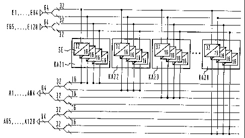
The switching network serves for the freely
selectable connecting of input lines (E1,...,E128)
combined into a plurality of input-line groups to at
least one output-line group (A1,...,A16), on the one hand
each of the input-line groups being connected to a
separate switching element (SE) of at least one arrangement
of switching elements (for example KA21) having a
funnel structure. On the other hand, the respective
arrangement of switching elements has a number of outputs
corresponding to the number of output lines belonging to
the respective output-line group. Each of these outputs
is in connection with one of the output lines belonging
to the respective output-line group. In this case, it is
provided that the respective arrangement of switching
elements (KA21) is formed only by the switching elements
(SE) connected to the input-line groups. The switching
elements in each case have outputs which are individually
assigned to the output lines belonging to the respective
output-line group. In this case, only one of the mutually
corresponding outputs of these switching elements can be
connected, according to choice, to the relevant output
line of the respect output-line group by switching means.


French Abstract

L'invention concerne une interface servant à connecter de manière sélective des lignes d'entrée (E1,..., E128) regroupées en une pluralité de groupes de lignes d'entrée, à au moins un groupe de lignes de sortie (A1,..., A16). Chacun des groupes de lignes d'entrée est connecté à un élément d'interface (SE) séparé d'au moins un agencement d'éléments d'interface (par ex. KA21) à structure conique. Chaque agencement d'éléments d'interface dispose d'un nombre de sorties correspondant au nombre de lignes de sortie appartenant à chaque groupe de lignes de sortie. Chacune de ces sorties est connectée à une des lignes de sortie appartenant au groupe de lignes de sortie correspondant. Il est prévu que chaque agencement d'éléments d'interface (KA21) ne comprenne que les éléments d'interface (SE) connectés aux groupes de lignes d'entrée. Les éléments d'interface disposent chacun de sorties associées individuellement aux lignes de sortie appartenant au groupe de lignes de sortie correspondant. Seule une des sorties de ces éléments d'interface, qui correspondent les unes aux autres, peut être connectée de manière sélective par des éléments de commutation à la ligne de sortie appropriée du groupe de lignes de sortie correspondant.

Claims

Note: Claims are shown in the official language in which they were submitted.


-8-


CLAIMS:


1. Switching network for communication devices for
the freely selectable connecting of input lines (E1,...,E128)
combined into a plurality of input-line groups to at least
one output-line group (A1,...,A16), on the one hand each of
the input-line groups being connected to a separate
switching element (SE) of at least one arrangement of
switching elements (for example KA21) having a funnel
structure and on the other hand the respective arrangement
of switching elements having a number of outputs
corresponding to the number of output lines belonging to the
respective output-line group and each of these outputs being
in connection with one of the output lines belonging to the
respective output-line group, characterized in that the
respective arrangement of switching elements (KA21) is
formed only by the switching elements (SE) connected to the
input-line groups, and in that each of the switching
elements has outputs which are individually assigned to the
output lines belonging to the respective output-line group,
and in that only one of the mutually corresponding outputs
of these switching elements can be selectively connected to
the relevant output-line of the respective output-line group
by switching means.

2. Switching network according to Claim 1,
characterized in that the switching means are of such a form
that the mutually corresponding outputs of the switching
elements are connected to each other by the said switching
means in the manner of a "wired-or" operation and each of
these outputs can be controlled, to assume an active or
high-impedance state.

3. Switching network according to Claim 1,
characterized in that tree switching means are in the form of


-9-


a multiplexing device (MUX) to which on the input side the
mutually corresponding outputs of the switching elements are
led and by which one of these outputs can be selectively
connected to the relevant output-line.

4. Switching network according to one of Claims 1 to
3, characterized in that the switching means are further of
such a form that differences in signal delay at the mutually
corresponding outputs of the switching elements are
compensated by the said switching means.

5. Switching network according to one of Claims 1 to
4, characterized in that a plurality of output-line groups
are provided, in that each of the output-line groups is
assigned a separate arrangement of switching elements and in
that the input-line groups are led in parallel to mutually
corresponding switching elements of the arrangement of
switching elements relevant for the said groups.


Description

Note: Descriptions are shown in the official language in which they were submitted.


CA 02233467 2001-11-08
20365-3823
-1-
Description
Switching network for communication devices
The invention .relates to a switching network for
communication devices fo_r the freely selectable connecting
of input lines combined.:into a plurality of input-line
groups to at least one output-line group according to the
precharacterizing clause of Patent Claim 1. Such a
switching network is already known from "IEEE JOURNAL ON
SELECTED AREAS IN COMMUNICATIONS", Vol. 9, No. 8, October
1991, pages 1299 to 1307. In the case of this switching
network, the respective arrangement of switching elements is
in a multi-stage form of funnel structure, in order to
connect an even number of input lines in a freely selectable
way to a number of output lines corresponding to half the
number of input lines. Consequently, due to the number of
individual switching elements for realizing the funnel
structure of the respective arrangement of switching
elements, relatively corrtplex circuitry is required, which is
sometimes undesired.
It is thus the' object of the present invention to
show a way in which a switching network according to the
precharacterizing clause of Patent Claim 1 can be formed to
make it possible to reduce the complexity of the circuitry
for realizing the respective arrangement of switching
elements.
In accordance with the present invention, there is
provided a switching nei~work for communication devices .for
the freely selectable connecting of input lines (E1,...,E128)
combined into a plurality of input-line groups to at least
one output-line group (A1,...,A16), on the one hand each of
the input-line groups being connected to a separate

CA 02233467 2001-11-08
20365-3823
-1a-
switching element (SE) o:E at least one arrangement of
switching elements (for s_°xample KA21) having a funnel
structure and on the other hand the respective arrangement
of switching elements having a number of outputs
corresponding to the num'oer of output lines belonging to the
respective output-line group and each of these outputs being
in connection with one of the output lines belonging to the
respective output-line group, characterized in that the
respective arrangement of switching elements (KA21) is
formed only by the switching elements (SE) connected to the
input-line groups, and i.n that each of the switching
elements has outputs which are individually assigned to the
output lines belonging to the respective output-line group,
and in that only one of the mutually corresponding outputs
of these switching elements can be selectively connected to
the relevant output-line of the respective output-line group
by switching means.
The invention thereby brings with it, for example,
the following advantages over the prior art:
- lower number of switching elements and
consequently a cost reduction for the respective arrangement
of switching elements,
- lower power loss because of the reduction in the
number of switching elements,

CA 02233467 1998-03-27
o ,
T T
95 P 2020 - 2 -
- saving in subassembly surface area for realizing the
switching network
- and lower signal delay time because of the reduced
number of switching elements to be passed through
within the respective arrangement of switching
elements.
Advantageous refinements of the switching network
according to the present invention emerge from Patent
Claims 2 to 5.
The present invention is described in more detail
below on the basis of exemplary embodiments represented
in the drawings, in which:
FIG 1 shows a switching network according to the prior
art cited above,
FIG 2 shows in schematic form a switching network in
which the present invention is used,
FIG 3 shows a first exemplary embodiment of the
arrangements of switching elements represented in
FIG 2,
FIG 4 shows a second exemplary embodiment of the
arrangements of switching elements represented in
FIG 2, and
FIG 5 shows an exemplary embodiment of arrangements of
switching elements according to FIG 2 distributed
between two subassemblies.
In FIG l, a switching network corresponding to
the prior art cited above is represented for the case in
which 128 input lines can be connected freely selectably
to 128 output lines. The input lines are denoted by El to
E128, the output lines on the other hand are denoted by
Al to A128. The input lines and output lines are in this
case subdivided into input-line groups and output-line
groups with in each case a fixed number of input lines
and output lines, respectively. An input-line group a.s
formed here by 32 input lines, an output-line group on
the other hand is formed by 16 output lines.
Altogether, in the assumed example, four input-
line groups and 8 output-line groups are formed. Each of
the 8 output-line groups is in this case assigned a

CA 02233467 1998-03-27
95 P 2020 - 3 -
separate arrangement of switching elements. The arrange-
ments of switching elements, which are denoted by KA11 to
KA18, are connected on the input side in parallel to the
four input-line groups.
The arrangements of switching elements, having
the same structure in each case, are respectively of a
multi-stage funnel form, using switching elements with 32
inputs and 16 outputs. The switching elements are denoted
by SE. A first stage has four switching elements, which
are in each case connected to one of the input-line
groups. This is adjoined by a second stage, which is
composed of two switching elements. To their inputs there
are led the outputs of the switching elements of the
first stage. On the output side, the switching elements
of the second stage are finally in connection with a
switching element forming a third stage. This switching
element is connected by its 16 outputs to one of the
output-line groups.
The switching network represented in FIG 1 and
realized in accordance with the prior art thus has in the
assumed example 7 switching elements per arrangement of
switching elements, ie. a total of 56 switching elements.
In FIG 2 there is represented a switching network
according to the present invention which can be used, for
example, in communication devices operating on the basis
of an asynchronous transfer mode (ATM), such as for
example ATM switching devices or ATM "cross connects", in
order to be able to relay information cells fixed for
this transfer mode. Apart from the realization of the
individual arrangements of switching elements, this
switching network corresponds to the switching network
reproduced in FIG 1. The arrangements of switching
elements are denoted in FIG 2 by KA21 to KA28. These
arrangements of switching elements are in each case of
only a single-stage form, four switching elements SE with
in each case 32 inputs and 16 outputs being provided in
this single stage. Here too, to each of these switching
elements there is connected one of the input-line groups.
The outputs of the switching elements are individually

CA 02233467 1998-03-27
95 P 2020 - 4 -
assigned to the 16 outputs of an output-line group.
However, in this case only one of the mutually correspon-
ding four outputs of the switching elements which are
assigned to one and the same output line can be con-
s netted, according to choice, to the relevant output line
by switching means.
In the case of the switching network represented
in FIG 2, there are thus required in the assumed example,
in contrast to the switching network reproduced in FIG 1,
now only four switching elements per arrangement of
switching elements and consequently a total of 32 switch-
ing elements.
In FIG 3 there is indicated a first exemplary
embodiment of how the individual arrangements of switch
ing elements represented in FIG 2 are realized. In the
case of this exemplary embodiment it is assumed that 64
input lines can be connected freely selectably to 16
output lines. For this purpose, two switching elements SE
with in each case 32 input lines and 16 output lines are
provided. In this case, the previously mentioned switch-
ing means are of such a form that the mutually corre-
sponding two outputs of the switching elements which are
assigned to one and the same output line are connected to
each other by the said switching means a.n the manner of
a "wired-or" operation. Each of these two outputs can be
controlled, according to choice, to assume an active or
high-impedence state, with the result that at a given
point is time only one of the two outputs is ever con-
nected to the relevant output line. Controlling takes
place in this case via a control bus CB connected to the
two switching elements. Via this control bus the outputs
of the switching elements are also controlled in such a
way that they operate bit-synchronously. The switching
over of the outputs of the switching elements connected
to each other by the switching means may in this case
take place, for example, after the transmission of an
information cell or when a so-called void cell occurs, if
void cells are inserted at periodically recurring inter-
vals in the cell stream to be relayed to the respective

CA 02233467 1998-03-27
95 P 2020 - 5 -
output line. Irrespective of the specific type of switch-
ing over, its sequence, and consequently the sequence for
the emiss3.on of an information cell by the respective
switching element, can be fixed by the respective switch-
ing element with the aid of control signals transmitted
via the control bus CB. For example, these control
signals may be sent commands which are cyclically emitted
to the switching elements.
In FIG 4 there is indicated a further exemplary
embodiment of how the individual arrangements of switch
ing elements represented in FIG 2 are realized. This
corresponds substantially to the exemplary embodiment
described before with reference to FIG 3. There is a
difference only in the design of the switching means for
switching the mutually corresponding outputs of the
switching elements SE to a relevant output line. While in
the case of the first exemplary embodiment a "wired-or"
operation is performed, here it is provided that the
switching elements are respectively followed by a multi-
plexa.ng device MUX. The two multiplexing devices MUX have
in the assumed example eight separate pairs of inputs,
which are each individually assigned an output connected
to one of the output lines. The multiplexing devices thus
have in each case an 8X2:1 structure. Connected to a pair
of inputs are in this case the two mutually corresponding
outputs of the switching elements SE assigned to one and
the same output line, the multiplexing devices being
controllable via the control bus CB a.n such a way that,
of a pair of inputs, at every point in time there a.s only
ever one input connected to the associated output line.
The sequence of the switching over may in this case take
place as in the case of the first exemplary embodiment by
control signals transmitted via the control bus. The
exemplary embodiment represented in FIG 4 may, moreover,
in the assumed example also be modified in such a way
that, instead of multiplexing devices individually
assigned to the switching elements, only one such multi-
plexing device a.s used, which in the example has 16 pairs
of inputs, to which in each case there is individually


CA 02233467 1998-03-27
95 P 2020 - 6 -
assigned an output. This multiplexing device thus has a
16X2:1 structure.
Finally, represented in FIG 5 is the case in
which, with an arrangement of switching elements, 128
input lines can be connected freely selectably to 16
output lines. Of the four switching elements SE required
for this purpose, in this case let two be accommodated on
a subassembly A, the remaining two switching element's on
the other hand be accommodated on a subassembly B. The
outputs of the two switching elements present on one
subassembly are in this case provided with switching
means according to one of the exemplary embodiments
explained above. Since differences in the delay during
the transmission of information cells may occur because
of this separate accommodation of the switching elements
and consequently because of different line lengths, the
outputs of the two subassemblies (16 per subassembly) are
connected to a phase-matching device PH, which is con-
nected on the output side to the 16 output lines. The
said differences in delay are compensated in this case by
this phase-matching device. In the event that the switch
ing means are in the form of multiplexing devices,
according to the second exemplary embodiment, the phase
matching may also be carried out by these multiplexing
devices.
Finally, a.t should also be pointed out that the
arrangements of switching elements explained above with
reference to Figures 2 to 5 only represent expedient
designs. For example, the switching elements respectively
included in the arrangements of switching elements may
also be modifed with regard to the number of inputs and
outputs. Moreover, the internal structure of the individ-
ual switching elements may, for example, be based on a
structure such as that specified in the document cited at
the beginning. In this case, all that is necessary is to
connect to the outputs of the respective switching
element switching means corresponding to one of the
exemplary embodiments explained above.
In addition, it should also be further pointed

CA 02233467 1998-03-27
95 P 2020 - 7 -
out that the switching network explained above can be
used not only in ATM communication devices but also
generally in communication devices which are designed for
a transmission principle other than the asynchronous
transfer mode mentioned.

Representative Drawing
A single figure which represents the drawing illustrating the invention.
Administrative Status

For a clearer understanding of the status of the application/patent presented on this page, the site Disclaimer , as well as the definitions for Patent , Administrative Status , Maintenance Fee  and Payment History  should be consulted.

Administrative Status

Title Date
Forecasted Issue Date 2004-06-22
(86) PCT Filing Date 1996-09-17
(87) PCT Publication Date 1997-04-03
(85) National Entry 1998-03-27
Examination Requested 1998-03-27
(45) Issued 2004-06-22
Deemed Expired 2008-09-17

Abandonment History

Abandonment Date Reason Reinstatement Date
2001-10-12 R30(2) - Failure to Respond 2001-11-08

Payment History

Fee Type Anniversary Year Due Date Amount Paid Paid Date
Request for Examination $400.00 1998-03-27
Registration of a document - section 124 $100.00 1998-03-27
Application Fee $300.00 1998-03-27
Maintenance Fee - Application - New Act 2 1998-09-17 $100.00 1998-08-17
Maintenance Fee - Application - New Act 3 1999-09-17 $100.00 1999-08-12
Maintenance Fee - Application - New Act 4 2000-09-18 $100.00 2000-08-18
Maintenance Fee - Application - New Act 5 2001-09-17 $150.00 2001-08-16
Reinstatement - failure to respond to examiners report $200.00 2001-11-08
Maintenance Fee - Application - New Act 6 2002-09-17 $150.00 2002-08-16
Maintenance Fee - Application - New Act 7 2003-09-17 $150.00 2003-08-14
Final Fee $300.00 2004-04-01
Maintenance Fee - Patent - New Act 8 2004-09-17 $200.00 2004-08-12
Maintenance Fee - Patent - New Act 9 2005-09-19 $200.00 2005-08-11
Maintenance Fee - Patent - New Act 10 2006-09-18 $250.00 2006-08-14
Owners on Record

Note: Records showing the ownership history in alphabetical order.

Current Owners on Record
SIEMENS AKTIENGESELLSCHAFT
Past Owners on Record
MARIGGIS, ATHANASE
Past Owners that do not appear in the "Owners on Record" listing will appear in other documentation within the application.
Documents

To view selected files, please enter reCAPTCHA code :


To view images, click a link in the Document Description column. To download the documents, select one or more checkboxes in the first column and then click the "Download Selected in PDF format (Zip Archive)" or the "Download Selected as Single PDF" button.

List of published and non-published patent-specific documents on the CPD .

If you have any difficulty accessing content, you can call the Client Service Centre at 1-866-997-1936 or send them an e-mail at CIPO Client Service Centre.


Document
Description 
Date
(yyyy-mm-dd) 
Number of pages   Size of Image (KB) 
Representative Drawing 1998-07-08 1 11
Claims 2001-11-08 2 71
Description 2001-11-08 8 343
Abstract 1998-03-27 1 33
Description 1998-03-27 7 309
Claims 1998-03-27 2 71
Drawings 1998-03-27 4 112
Cover Page 1998-07-08 2 76
Abstract 2004-04-02 1 33
Cover Page 2004-05-18 1 54
Representative Drawing 2004-05-18 1 14
PCT 1998-03-27 6 230
PCT 1998-04-08 5 155
Assignment 1998-03-27 3 135
Prosecution-Amendment 2001-04-12 2 37
Prosecution-Amendment 2001-11-08 7 216
Correspondence 2004-04-01 1 31