Note: Descriptions are shown in the official language in which they were submitted.
CA 02254525 2002-05-15
74935-19
BUS MONITORING SYSTEM
BACKGROUND OF THE INVENTION
1. Field of the Invention
The present invention relates to a bus monitoring
system and particularly, to a bus monitoring system for
monitoring the operation status of a microprocessor.
2. Description of the Prior Art
There is disclosed a multi-chip module evaluating
device in, for example, Japanese Patent Laid-Open No. 5-
120160 (1993), which monitors signals on wires of a multi-
chip module between a floating operation unit and a data
memory. The signals on the wires which are embedded in the
module substrate of a multi-chip module are monitored by
connecting, via a probe, a leader pad on the module
substrate with a monitor unit which comprises a memory, an
address generator, and a comparator. This evaluating device
can monitor directly the signals on the wires, without using
any test element group (TEG). Therefore, this evaluating
device is employed for monitoring the signals on the wires,
because an evaluation using only signals extracted to
external pins is not sufficient, in case of large scale
integration (LSI) packages mounted on the module substrate.
In this connection, the above-mentioned
conventional device has the following disadvantages:
Firstly, leader pads are necessary for monitoring
the signals on the wires because the signals on the wires
are imbedded in the module substrate. Accordingly, the
above-mentioned evaluating device is not of any use for a
small sized multi-chip module, because the number of pads
increases with the increase in the number of wires in the
1
CA 02254525 2005-02-03
74935-19
module substrate, which results in the increase in the area
required for pads.
Secondly, a testing device is necessary
exclusively for bus monitoring. Specially designed probes
are required for connection to the special leader pads on
the module substrate.
Thirdly, the reliability of bus monitoring is
lowered. When the leader pads are inferior due to a
manufacturing process, then the module substrate can not be
monitored completely.
SUMMARY OF THE INVENTION
Therefore, an object of the present invention is
to provide a bus monitoring system with improved reliability
for monitoring easily the bus of a microprocessor via bus
interface, when evaluating bus interface peripheral circuits
and the software for a microprocessor board. Another object
of the present invention is to improve the reliability of
the evaluation system.
According to the present invention, there is
provided a bus monitoring system which comprises: a
microprocessor; an internal bus comprising address lines,
data lines and control signal lines; a main memory which is
connected to said microprocessor via said internal bus; a
system control register which is connected to said
microprocessor via said internal bus; a bus interface which
is connected to said microprocessor via said internal bus;
an external bus which is connected to said internal bus via
said bus interface; wherein said bus interface outputs the
same signal as the signal on said address lines to first
lines of said external bus and the same signal as the signal
on said data lines to second lines of said external bus,
2
CA 02254525 2007-01-11
74935-19
said first lines being different from said second lines, and
wherein said bus interface outputs an address strobe signal
which indicates whether or not signals on said address lines
are valid and a data ready signal which indicates whether or
not signals on said data lines are valid, and wherein said
data ready signal is a detection signal of a negative edge
of a CAS signal.
2a
CA 02254525 2004-02-09
74935-19
In the bus monitoring system, the bus interface
may output an address strobe signal which indicates whether
or not signals on the address lines are valid and a data
ready signal which indicates whether or not signals on the
data lines are valid.
According to the present invention as explained
above, the following effects are obtained:
Firstly, the leader pads become unnecessary for
monitoring the signals on the wires which are imbedded in a
module substrate, because every status of an internal bus
can be monitored via the bus interface.
Secondly, a high density mounting board such as a
multi-chip module can be furthermore integrated in a higher
density system, while keeping the capability of the internal
bus monitoring, because the leader pads become unnecessary
and the wide mounting area for other purposes is preserved.
Thirdly, bus monitoring becomes easy, because
ordinary available instruments can be used for bus
monitoring at the external bus connected with bus interface,
or the peripheral circuit of a microprocessor board.
BRIEF EXPLANATION OF THE DRAWINGS
Figure 1 is a block diagram of a bus monitoring
system of an embodiment of the present invention.
Figure 2 is a timing chart for explaining the
action of the bus monitoring system of an embodiment of the
present invention.
3
CA 02254525 2002-05-15
74935-19
PREFERRED EMBODIMENT OF THE INVENTION
A preferred embodiment of the present invention is
explained. The microprocessor board of the bus monitoring
system of the present invention comprises an internal bus
which comprise a microprocessor, address lines, data lines,
and control signal lines, a main memory connected via the
internal bus with the microprocessor, registers such as a
system control register, and a bus interface circuit. Every
access to the main memory, the system control register, and
the bus interface by the microprocessor is outputted to an
external bus via the bus interface circuit. Accordingly,
the operation status of the microprocessor or the internal
bus can be monitored by monitoring the external bus.
Referring to the accompanying drawings, a working
example of the present invention is explained to clarify the
embodiment of the present invention.
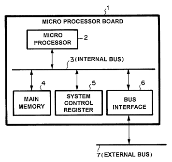
As shown in Figure 1, a microprocessor board 1
comprises a microprocessor 2 connected with an internal bus
3, a main memory 4, a system control register 5 and a bus
interface 6. Further, the microprocessor board 1 is
connected with an external bus 7 via the bus interface 6.
Next, referring to Figure 1, the action of the
microprocessor board 1 of the working example is explained.
The microprocessor 2 accesses the main memory 4
and the system control register 5 via the internal bus 3.
Therefore, every access in the microprocessor board 1 can be
monitored by monitoring the internal bus 3.
The bus interface 6 outputs addresses, data, and
control signals from the internal bus 3 to the external bus
4
CA 02254525 2002-05-15
74935-19
7, when the microprocessor 2 executes a write access to main
memory 4, or the system control register 5.
Also, the bus interface 6 outputs addresses, data,
and control signals from the internal bus 3 to the external
bus 7, when the microprocessor 2 executes a read access to
the main memory 4, or the system control register 5.
Thus, the internal bus 3 can be monitored by
monitoring the external bus 7. In other words, the
execution process of a program of the microprocessor 2
mounted on the microprocessor board 1 can be traced by
monitoring the external bus 7 since all address, data and
control signals on the internal bus 3 are output to the
external bus 7.
Referring to Figure 2, the action of the bus
interface 6 between the internal bus 3 and the external bus
7 of the working example is explained.
The action of a two word write into main memory 4
by the microprocessor 2 shown in Figure 1, is shown
concretely in Figure 2.
The internal bus 3 executes a write access to the
main memory 4, carrying an internal bus address 10 and an
internal bus write data 11 in the microprocessor 2.
The main memory 4 accepts the internal bus address
10 and the internal bus write data 11 and writes them by
using a row address strobe (RAS) control signal 12 and a
column address strobe (CAS) control signal 13, while the bus
interface 6 outputs the same address as the internal bus
address 10 as an external bus address 14. At the same time,
the bus interface 6 outputs an external bus strobe 15 to
validate the external bus address 14.
5
CA 02254525 2002-05-15
74935-19
The bus interface 6 outputs an external bus data
16 which is the same as an internal bus data 11. At the
same time, the bus interface 6 outputs an external bus data
ready 17 synchronized with the CAS control signal 13.
Thus, an effective timing of a write address and
write data are confirmed by the external bus 7, when the
microprocessor 2 executes a write access to the main memory
4.
Similarly, an effective timing of a read address
and read data are confirmed by the external bus 7, when the
microprocessor 2 executes a read access to the main memory
4. The accesses to the system control register 5 are
confirmed similarly. Thus, the internal bus 3 can be
monitored by the external bus 7.
6