Note: Descriptions are shown in the official language in which they were submitted.
CA 0226091~ l999-01-l~
W098/0~38 PCT/SE97/01169
A METHOD AND DEVICE FOR CONTINUOUS-TIME FILTERING IN DIGITAL
CMOS PROCESS
FIELD OF THE INVENTION
The present invention relates to a method for continuous-time
filtering in digital CMOS process and a device ror continuous-
time filtering in digital CMOS process.
BACKGROUND OF TEE INVENTION
It is of importance to design a mixed analog/digital system in
digital CMOS process concerning processing cost, testing cost
and performance. There has been strong interect in designing
sampled data systems, e.g. switched-current filters and data
converter in digital CMOS processes, see for example C.
Toumazou, J.B. Hughes, and N.C. Battersby (E~s), "Switched-
Currents: an Analogue Technique for Digital Technology,", Peter
Peregrinus Ltd., 1993, and N. Tan, "Switched-current delta-sigma
A/D converters", J. Analog Integrated Circu~ts and Signal
Processing, Jan. 1996, pp 7-24. However, to utilize these kind
of techniques, antialiasing filters are usually needed before
sampling the analog input in order to avoid aliasing.
Traditionally, a separate chip using analog C~OS process or
discrete RC filter circuitry is used. Obviously, integrating the
continuous-time filters, or antialiasing filters with sampled
data systems and DSP circuits on the same chip offers the best
performance/cost ratio.
In, for example, N. Tan and M. Gustavsson, Voltage-to-current
converter", pending US patent application No. 08/646,964, May 8,
CA 0226091~ Ig99-01-1~
W098/04038 PCT/SE97/01169
1996, a method was specifically developed to realize a low-pass
filtering function embedded with a voltage-to-current
conversion.
In, for example, US-A-4,839,542 there are disclosed active
transconduc-tance.filters, which belong to a filter type which is
called a transconductance-capacitance (gm-C) filter. The basic
idea is to create poles by using linear capacitors and
transconductors. As for most active components, current mirrors
are used as active loads for the transconductors and current
mirrors are not utilized to create poles for any filtering
purposes.
In W095/06977, current mirrors are disclosed and only used as
active loads to increase the gain for the amplifier. As a matter
of fact, for most gain stages, current mirrors are used as
active loads to increase the gain.
In US-A-4,686,487 there is disclosed how to design current
mirrors for amplifiers in order to have high speed operation.
The pole due to the current mirror is parasitic and the means of
adding a resistor is invented to reduce the effect on high speed
operation.
SIJ~$ARY OF THE INVENl~ION
The invention relates preferably to the design of continuous-
time filters for sampled data systems in digital CMOS processes.
In a digital CMOS process neither resistors nor linear
capacitors are available. Therefore it is not possible or simply
not practical to design continuous-time filters using
CA 0226091~ Ig99-01-1~
W098/04038 PCT/SE97/01169
traditional methods. It has been proposed to utilize current
mirrors to realize filtering functions in a voltage-to-current
converter. The pole frequency is therefore determined by the
~ transconductance of an MOS transistor and the capacitance seen
at its gate. In this application, a generalized method of
designing continuous-time filters in digital CMOS process and
methods of cascading have been proposed to reduce the spread of
the pole frequencies.
BRIEF DESCRIPTION OF THE DRAWINGS
Fig. l is a circuit showing a basic current mirror as a single-
pole filter.
Fig. 2 is a graph showing SPICE simulation results of fig. l,
wherein cascode current mirrors and cascode current sources are
used and the capacitor is realized by NMOS transistors.
Fig. 3 a and b are circuits showing cascading techniques
according to the invention.
Fig. 4 is a graph showing SPICE simulation results of fig. 3b,
wherein cascode current mirrors and cascode current sources are
used and the capacitors are realized by NMOS transistors.
BRIEF DESCRIPTION OF THE PREFERRED EMBODIMENTS
In digital CMOS processes, neither resistors nor linear
capacitors are available. Though it is possible to utilize the
gate poly as resistors, the sheet resistance is very small and
has large variation for a sub-micro CMOS process, and well
resistors are sensitive to noise and have large variation as
well. Therefore, active components are intended to be used, i.e.
transistors, to realize resistance. Though it is possible to
CA 0226091~ 1999-01-1~
WO 98/04038 PCT/SE97/01169
utilize the single poly layer and metallizations to realize a
linear capacitor, the sheet capacitance is very small in a sub-
micron CMOS process. Therefore, the gate capacitance is intended
to be utilized, which has much larger sheet capacitance. The
basic current mirror used as a single-pole low pass filter is
shown in ~ig. 1.
The capacitor C0 1 can be realized by a gate capacitor on chip,
or realized hy an off-chip capacitor, if the cut-off frequency
of the filter is required to be very low. By properly
dimensioning the sizes of transistors Mo 2 and Ml 3 and their
associated bias currents ~, 5, a scaling factor can also be
realized within this filter.
The pole frequency of the single-pole filter shown in fig. 1 is
given by
g",o
fo 2~ C0+ Cp0
where gm0 is the transconductance of the diode-connected
transistor Mo 2 and Cp0 represents all the parasitics at the gate
of transistor Mo 2.
The nonlinearities in the transconductances do not introduce
distortion in the output current as long as the
transconductances of Mo 2 and Ml 3 are matched or constantly
rationed. However, nonlinearities in the capacitance can
introduce error in the output current. Though the gate
capacitance is highly nonlinear across the whole operation
region, in a current mirror configuration as shown in fig. 1,
CA 0226091~ Ig99-01-1~
WO98N4038 PCT/SE97/01169
the gate voltage change is quite limited, making the transistors
operate in a well specified region all the time. Therefore, the
gate capacitance does not vary dramatically and the linearity is
acceptable. When external capacitors are used, linearity can
also be guaranteed.
However, the transconductance of a transistor is dependent of
the drain current, i.e.,
W
g~ 2~L"C,~T LiD,
where ~n is the channel charge mobility, COX is the unit gate
capacitance, W/L is the transistor size, and iD is the drain
current. Therefore, when the drain current in transistor Mo 2
changes accommodating input current Io~ the transconductance gmO
changes, making the pole frequency change. In fig. 2 it is shown
the SPICE simulation results, when the input current changes
between +0,5 IbiasO
It can be seen that the circuit of fig. l is a single-pole
system, having 20 dB/dec frequency roll-off. And the change in
the 3-dB frequency is well in line with the prediction given by
the equation of transconductance. The change in the pole
frequency also introduces distortion, when the input signal
frequency approaches the cut-off frequency, in that a different
input amplitude experiences a different attenuation.
The simulated total harmonic distortion is about -50 dB, when
the input is a lO0 Khz sinusoidal with amplitude equal to one-
fourth of the bias current. When the input freauency decreases
CA 0226091~ Ig99-01-1~
W098/04038 6 PCT/SE97/01169
to l0 Khz, the total harmonic distortion is less than -70 dB.
When the input frequency is larger than the cut-off frequency,
the total harmonic distortion is attenuated by the filter
itself.
obviously, to make the pole frequency well-defined, the change
in the drain current is needed to be as small as possible. One
way to do so is to limit the input current compared with the
bias current. This is very power consuming. However, proper
cascading realizing higher-order filters can reduce the
variation in the pole frequencies.
To increase the filter order and reduce the variation in pole
frequencies cascading of current mirrors can be used. A single-
pole system only gives a 20-dB/dec roll-off. In many
applications, sharper cut-off is needed. Cascading two single-
pole systems realizes a two-pole system having a 40-dB/dec roll-
off. Sharper cut-off can be realized by cascading more stages.
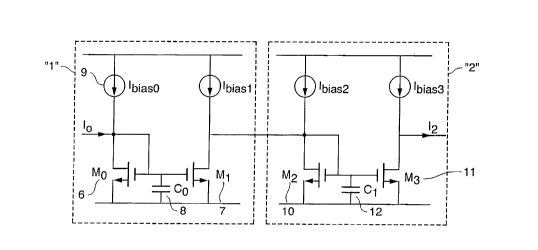
There are two possibilities of cascading as shown in fig. 3a and
b.
The use of cascading shown in fig. 3a results in lower power
consumption due to the use of the p-type branch. The n-type
branch "l" consists of n-type transistors M0 6 and Ml 7,
capacitor C0 8 and bias current IbiasO 9 for transistor M0 6.
The p-type branch "2" consists of p-type transistors M2 l0 and
M3 ll capacitor Cl 12 and bias current Ibiasl 13 for M3 ll. The
n-type branch is similar to the one shown in fig. l except that
the bias current for Ml 7 is omitted due to the use of the p-
type branch. Transistors Ml 7 and M2 l0 bias each other. The p-
type branch is the same as the n-type except p-type transistors
CA 0226091~ Ig99-01-1~
W098/04038 PCTISE97/01169
are used. However, this kind of cascading influences the pole
frequencies. Suppose that input current Io is positive, then the
drain current in Mo 6 increases making its transconductance to
increase. Therefore, the pole frequency determined by the
transconductance of Mo 6 and capacitor C0 8 will increase. At
the same time, the drain current in M2 lO, equal to the drain
current of M1 7, increases as well making its transconductance
to increase. Therefore, the pole frequency determined by the
transconductance of M2 lO and the capacitance of Cl 12 will
increase as well. The combined effect is that the pole
frequencies vary more rapidly as the input current varies.
The cascading technique shown in fig. 3 b results in more power
consumption due to an extra n-type branch. It consists of two n-
type branches "l" and "2", which are exactly the same as the oneshown in fig. l. However, it has a big advantage stabilizing the
pole frequencies. Suppose that input current Io is positive,
then the drain current in M0 6 increases making its
transconductance increase. Therefore, the pole frequency
determined by g~0/C0 will increase. At the same time, the drain
current in M2 lO decreases making its transconductance decrease.
Therefore, the pole frequency determined by g~2/C1 will decrease.
The combined effect is that the variations in the two pole
frequencies tend to reduce the total variation.
In fig. 4 the SPICE simulation results are shown, when the input
current changes between +0,5 Ibiaso.
It can be seen that the circuit of fig. 3b is a two-pole system,
having 40-dB/dec frequency roll-off. And the change in the
variation in the 3-dB frequency is reduced considerably.
CA 0226091~ I999-ol-l~
W098/04038 PCT/SE97/01169
The simulated total harmonic distortion is less than - 60 dB,
when the input is a 100 Khz sinusoidal with amplitude equal to
one-fourth of the bias current. When the input frequency
decreases to 10 Khz, the total harmonic distortion is less than
-80 dB. When the input frequency is larger than the cut-off
frequency, the total harmonic distortion is attenuated by the
filter itself.
While the foregoing description includes numerous details and
specificities, it is to be understood that these are merely
illustrative of the present invention, and are not to be
construed as limitations. Many modifications will be readily
apparent to those skilled in the art, which do not depart from
the spirit and scope of the invention as defined by the appended
claims and their legal equivalents.