Sélection de la langue

Search

Sommaire du brevet 2260915 

Énoncé de désistement de responsabilité concernant l'information provenant de tiers

Une partie des informations de ce site Web a été fournie par des sources externes. Le gouvernement du Canada n'assume aucune responsabilité concernant la précision, l'actualité ou la fiabilité des informations fournies par les sources externes. Les utilisateurs qui désirent employer cette information devraient consulter directement la source des informations. Le contenu fourni par les sources externes n'est pas assujetti aux exigences sur les langues officielles, la protection des renseignements personnels et l'accessibilité.

Disponibilité de l'Abrégé et des Revendications

L'apparition de différences dans le texte et l'image des Revendications et de l'Abrégé dépend du moment auquel le document est publié. Les textes des Revendications et de l'Abrégé sont affichés :

  • lorsque la demande peut être examinée par le public;
  • lorsque le brevet est émis (délivrance).
(12) Demande de brevet: (11) CA 2260915
(54) Titre français: TECHNIQUE DE FILTRAGE EN CONTINU ET DISPOSITIF CORRESPONDANT EN TECHNOLOGIE CMOS NUMERIQUE
(54) Titre anglais: A METHOD AND DEVICE FOR CONTINUOUS-TIME FILTERING IN DIGITAL CMOS PROCESS
Statut: Réputée abandonnée et au-delà du délai pour le rétablissement - en attente de la réponse à l’avis de communication rejetée
Données bibliographiques
(51) Classification internationale des brevets (CIB):
  • H03F 03/45 (2006.01)
  • H03F 03/345 (2006.01)
  • H03H 11/04 (2006.01)
(72) Inventeurs :
  • TAN, NIANXIONG (Suède)
(73) Titulaires :
  • TELEFONAKTIEBOLAGET LM ERICSSON
(71) Demandeurs :
  • TELEFONAKTIEBOLAGET LM ERICSSON (Suède)
(74) Agent: MARKS & CLERK
(74) Co-agent:
(45) Délivré:
(86) Date de dépôt PCT: 1997-06-27
(87) Mise à la disponibilité du public: 1998-01-29
Requête d'examen: 2002-06-03
Licence disponible: S.O.
Cédé au domaine public: S.O.
(25) Langue des documents déposés: Anglais

Traité de coopération en matière de brevets (PCT): Oui
(86) Numéro de la demande PCT: PCT/SE1997/001169
(87) Numéro de publication internationale PCT: SE1997001169
(85) Entrée nationale: 1999-01-15

(30) Données de priorité de la demande:
Numéro de la demande Pays / territoire Date
9602824-6 (Suède) 1996-07-19

Abrégés

Abrégé français

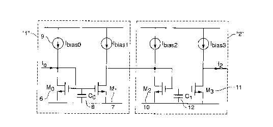
En technologie CMOS numérique, on ne peut utiliser ni les résistances ni les condensateurs linéaires et il est impossible ou tout simplement malaisé de concevoir des filtres à temps continu en faisant appel aux méthodes classiques. L'idée a donc été émise d'utiliser des miroirs de courant pour effectuer des filtrages dans un convertisseur tension-courant en concevant des filtres à temps continu pour des systèmes de données échantillonnés dans le cadre d'une technologie CMOS numérique. On détermine donc la fréquence d'un pôle au moyen de la transconductance d'un transistor à effet de champ métal-oxyde semi-conducteur (MOS) (6) et de la capacité d'un condensateur (8) mesurée à la grille du transistor. Il est décrit, au titre de cette invention, un procédé général de conception de filtres à temps continu dans le cadre d'une technologie CMOS ainsi que des techniques de cascadage afin de réduire l'étalement des fréquences d'un pôle.


Abrégé anglais


In a digital CMOS process neither resistors nor linear capacitors are
available and it is not possible or simply not practical to design continuous-
time filters using traditional methods. It has therefore been proposed to
utilize current mirrors to realize filtering functions in a voltage-to-current
converter when designing continuous-time filters for sampled data systems in
digital CMOS processes. The pole frequency is therefore determined by the
transconductance of an MOS transistor (6) and the capacitance of a capacitor
(8) seen at its gate. In this application, a generalized method of designing
continuous-time filters in digital CMOS process and methods of cascading have
been proposed to reduce the spread of the pole frequencies.

Revendications

Note : Les revendications sont présentées dans la langue officielle dans laquelle elles ont été soumises.


CLAIMS
1. A device for continuous-time filtering in a digital CMOS
process, where current mirrors are used to realize continuous-time
filters in a digital CMOS process and pole frequencies are
determined by a transconductance of an MOS transistor and a
capacitance of a capacitor seen by its gate, wherein the
capacitance defining the pole frequency can take any form
including an off-chip capacitor, characterized in
that a current mirror consisting of transistors M0 (6), M1 (7)
and a gate capacitor or off-chip capacitor C0 (8) are used to
determine the pole frequency.
2. A device according to claim 1, characterized in
that two or more current mirrors are provided to be cascaded to
realize higher order filters and in that n-type ("1") and p-type
("2") current mirrors are provided to be alternate to save power
dissipation.
3. A device according to claim 1, characterized in
that two or more current mirrors are provided to be directly
cascaded to realize higher order filters and to reduce the
spread in pole frequencies by only using n-type or p-type
current mirrors.

Description

Note : Les descriptions sont présentées dans la langue officielle dans laquelle elles ont été soumises.


CA 0226091~ l999-01-l~
W098/0~38 PCT/SE97/01169
A METHOD AND DEVICE FOR CONTINUOUS-TIME FILTERING IN DIGITAL
CMOS PROCESS
FIELD OF THE INVENTION
The present invention relates to a method for continuous-time
filtering in digital CMOS process and a device ror continuous-
time filtering in digital CMOS process.
BACKGROUND OF TEE INVENTION
It is of importance to design a mixed analog/digital system in
digital CMOS process concerning processing cost, testing cost
and performance. There has been strong interect in designing
sampled data systems, e.g. switched-current filters and data
converter in digital CMOS processes, see for example C.
Toumazou, J.B. Hughes, and N.C. Battersby (E~s), "Switched-
Currents: an Analogue Technique for Digital Technology,", Peter
Peregrinus Ltd., 1993, and N. Tan, "Switched-current delta-sigma
A/D converters", J. Analog Integrated Circu~ts and Signal
Processing, Jan. 1996, pp 7-24. However, to utilize these kind
of techniques, antialiasing filters are usually needed before
sampling the analog input in order to avoid aliasing.
Traditionally, a separate chip using analog C~OS process or
discrete RC filter circuitry is used. Obviously, integrating the
continuous-time filters, or antialiasing filters with sampled
data systems and DSP circuits on the same chip offers the best
performance/cost ratio.
In, for example, N. Tan and M. Gustavsson, Voltage-to-current
converter", pending US patent application No. 08/646,964, May 8,

CA 0226091~ Ig99-01-1~
W098/04038 PCT/SE97/01169
1996, a method was specifically developed to realize a low-pass
filtering function embedded with a voltage-to-current
conversion.
In, for example, US-A-4,839,542 there are disclosed active
transconduc-tance.filters, which belong to a filter type which is
called a transconductance-capacitance (gm-C) filter. The basic
idea is to create poles by using linear capacitors and
transconductors. As for most active components, current mirrors
are used as active loads for the transconductors and current
mirrors are not utilized to create poles for any filtering
purposes.
In W095/06977, current mirrors are disclosed and only used as
active loads to increase the gain for the amplifier. As a matter
of fact, for most gain stages, current mirrors are used as
active loads to increase the gain.
In US-A-4,686,487 there is disclosed how to design current
mirrors for amplifiers in order to have high speed operation.
The pole due to the current mirror is parasitic and the means of
adding a resistor is invented to reduce the effect on high speed
operation.
SIJ~$ARY OF THE INVENl~ION
The invention relates preferably to the design of continuous-
time filters for sampled data systems in digital CMOS processes.
In a digital CMOS process neither resistors nor linear
capacitors are available. Therefore it is not possible or simply
not practical to design continuous-time filters using

CA 0226091~ Ig99-01-1~
W098/04038 PCT/SE97/01169
traditional methods. It has been proposed to utilize current
mirrors to realize filtering functions in a voltage-to-current
converter. The pole frequency is therefore determined by the
~ transconductance of an MOS transistor and the capacitance seen
at its gate. In this application, a generalized method of
designing continuous-time filters in digital CMOS process and
methods of cascading have been proposed to reduce the spread of
the pole frequencies.
BRIEF DESCRIPTION OF THE DRAWINGS
Fig. l is a circuit showing a basic current mirror as a single-
pole filter.
Fig. 2 is a graph showing SPICE simulation results of fig. l,
wherein cascode current mirrors and cascode current sources are
used and the capacitor is realized by NMOS transistors.
Fig. 3 a and b are circuits showing cascading techniques
according to the invention.
Fig. 4 is a graph showing SPICE simulation results of fig. 3b,
wherein cascode current mirrors and cascode current sources are
used and the capacitors are realized by NMOS transistors.
BRIEF DESCRIPTION OF THE PREFERRED EMBODIMENTS
In digital CMOS processes, neither resistors nor linear
capacitors are available. Though it is possible to utilize the
gate poly as resistors, the sheet resistance is very small and
has large variation for a sub-micro CMOS process, and well
resistors are sensitive to noise and have large variation as
well. Therefore, active components are intended to be used, i.e.
transistors, to realize resistance. Though it is possible to

CA 0226091~ 1999-01-1~
WO 98/04038 PCT/SE97/01169
utilize the single poly layer and metallizations to realize a
linear capacitor, the sheet capacitance is very small in a sub-
micron CMOS process. Therefore, the gate capacitance is intended
to be utilized, which has much larger sheet capacitance. The
basic current mirror used as a single-pole low pass filter is
shown in ~ig. 1.
The capacitor C0 1 can be realized by a gate capacitor on chip,
or realized hy an off-chip capacitor, if the cut-off frequency
of the filter is required to be very low. By properly
dimensioning the sizes of transistors Mo 2 and Ml 3 and their
associated bias currents ~, 5, a scaling factor can also be
realized within this filter.
The pole frequency of the single-pole filter shown in fig. 1 is
given by
g",o
fo 2~ C0+ Cp0
where gm0 is the transconductance of the diode-connected
transistor Mo 2 and Cp0 represents all the parasitics at the gate
of transistor Mo 2.
The nonlinearities in the transconductances do not introduce
distortion in the output current as long as the
transconductances of Mo 2 and Ml 3 are matched or constantly
rationed. However, nonlinearities in the capacitance can
introduce error in the output current. Though the gate
capacitance is highly nonlinear across the whole operation
region, in a current mirror configuration as shown in fig. 1,

CA 0226091~ Ig99-01-1~
WO98N4038 PCT/SE97/01169
the gate voltage change is quite limited, making the transistors
operate in a well specified region all the time. Therefore, the
gate capacitance does not vary dramatically and the linearity is
acceptable. When external capacitors are used, linearity can
also be guaranteed.
However, the transconductance of a transistor is dependent of
the drain current, i.e.,
W
g~ 2~L"C,~T LiD,
where ~n is the channel charge mobility, COX is the unit gate
capacitance, W/L is the transistor size, and iD is the drain
current. Therefore, when the drain current in transistor Mo 2
changes accommodating input current Io~ the transconductance gmO
changes, making the pole frequency change. In fig. 2 it is shown
the SPICE simulation results, when the input current changes
between +0,5 IbiasO
It can be seen that the circuit of fig. l is a single-pole
system, having 20 dB/dec frequency roll-off. And the change in
the 3-dB frequency is well in line with the prediction given by
the equation of transconductance. The change in the pole
frequency also introduces distortion, when the input signal
frequency approaches the cut-off frequency, in that a different
input amplitude experiences a different attenuation.
The simulated total harmonic distortion is about -50 dB, when
the input is a lO0 Khz sinusoidal with amplitude equal to one-
fourth of the bias current. When the input freauency decreases

CA 0226091~ Ig99-01-1~
W098/04038 6 PCT/SE97/01169
to l0 Khz, the total harmonic distortion is less than -70 dB.
When the input frequency is larger than the cut-off frequency,
the total harmonic distortion is attenuated by the filter
itself.
obviously, to make the pole frequency well-defined, the change
in the drain current is needed to be as small as possible. One
way to do so is to limit the input current compared with the
bias current. This is very power consuming. However, proper
cascading realizing higher-order filters can reduce the
variation in the pole frequencies.
To increase the filter order and reduce the variation in pole
frequencies cascading of current mirrors can be used. A single-
pole system only gives a 20-dB/dec roll-off. In many
applications, sharper cut-off is needed. Cascading two single-
pole systems realizes a two-pole system having a 40-dB/dec roll-
off. Sharper cut-off can be realized by cascading more stages.
There are two possibilities of cascading as shown in fig. 3a and
b.
The use of cascading shown in fig. 3a results in lower power
consumption due to the use of the p-type branch. The n-type
branch "l" consists of n-type transistors M0 6 and Ml 7,
capacitor C0 8 and bias current IbiasO 9 for transistor M0 6.
The p-type branch "2" consists of p-type transistors M2 l0 and
M3 ll capacitor Cl 12 and bias current Ibiasl 13 for M3 ll. The
n-type branch is similar to the one shown in fig. l except that
the bias current for Ml 7 is omitted due to the use of the p-
type branch. Transistors Ml 7 and M2 l0 bias each other. The p-
type branch is the same as the n-type except p-type transistors

CA 0226091~ Ig99-01-1~
W098/04038 PCTISE97/01169
are used. However, this kind of cascading influences the pole
frequencies. Suppose that input current Io is positive, then the
drain current in Mo 6 increases making its transconductance to
increase. Therefore, the pole frequency determined by the
transconductance of Mo 6 and capacitor C0 8 will increase. At
the same time, the drain current in M2 lO, equal to the drain
current of M1 7, increases as well making its transconductance
to increase. Therefore, the pole frequency determined by the
transconductance of M2 lO and the capacitance of Cl 12 will
increase as well. The combined effect is that the pole
frequencies vary more rapidly as the input current varies.
The cascading technique shown in fig. 3 b results in more power
consumption due to an extra n-type branch. It consists of two n-
type branches "l" and "2", which are exactly the same as the oneshown in fig. l. However, it has a big advantage stabilizing the
pole frequencies. Suppose that input current Io is positive,
then the drain current in M0 6 increases making its
transconductance increase. Therefore, the pole frequency
determined by g~0/C0 will increase. At the same time, the drain
current in M2 lO decreases making its transconductance decrease.
Therefore, the pole frequency determined by g~2/C1 will decrease.
The combined effect is that the variations in the two pole
frequencies tend to reduce the total variation.
In fig. 4 the SPICE simulation results are shown, when the input
current changes between +0,5 Ibiaso.
It can be seen that the circuit of fig. 3b is a two-pole system,
having 40-dB/dec frequency roll-off. And the change in the
variation in the 3-dB frequency is reduced considerably.

CA 0226091~ I999-ol-l~
W098/04038 PCT/SE97/01169
The simulated total harmonic distortion is less than - 60 dB,
when the input is a 100 Khz sinusoidal with amplitude equal to
one-fourth of the bias current. When the input frequency
decreases to 10 Khz, the total harmonic distortion is less than
-80 dB. When the input frequency is larger than the cut-off
frequency, the total harmonic distortion is attenuated by the
filter itself.
While the foregoing description includes numerous details and
specificities, it is to be understood that these are merely
illustrative of the present invention, and are not to be
construed as limitations. Many modifications will be readily
apparent to those skilled in the art, which do not depart from
the spirit and scope of the invention as defined by the appended
claims and their legal equivalents.

Dessin représentatif
Une figure unique qui représente un dessin illustrant l'invention.
États administratifs

2024-08-01 : Dans le cadre de la transition vers les Brevets de nouvelle génération (BNG), la base de données sur les brevets canadiens (BDBC) contient désormais un Historique d'événement plus détaillé, qui reproduit le Journal des événements de notre nouvelle solution interne.

Veuillez noter que les événements débutant par « Inactive : » se réfèrent à des événements qui ne sont plus utilisés dans notre nouvelle solution interne.

Pour une meilleure compréhension de l'état de la demande ou brevet qui figure sur cette page, la rubrique Mise en garde , et les descriptions de Brevet , Historique d'événement , Taxes périodiques et Historique des paiements devraient être consultées.

Historique d'événement

Description Date
Inactive : CIB de MCD 2006-03-12
Le délai pour l'annulation est expiré 2005-06-27
Demande non rétablie avant l'échéance 2005-06-27
Inactive : Abandon. - Aucune rép dem par.30(2) Règles 2004-07-20
Inactive : Abandon. - Aucune rép. dem. art.29 Règles 2004-07-20
Réputée abandonnée - omission de répondre à un avis sur les taxes pour le maintien en état 2004-06-28
Inactive : Dem. de l'examinateur art.29 Règles 2004-01-20
Inactive : Dem. de l'examinateur par.30(2) Règles 2004-01-20
Lettre envoyée 2002-07-22
Exigences pour une requête d'examen - jugée conforme 2002-06-03
Requête d'examen reçue 2002-06-03
Toutes les exigences pour l'examen - jugée conforme 2002-06-03
Inactive : CIB en 1re position 1999-03-29
Symbole de classement modifié 1999-03-29
Inactive : CIB attribuée 1999-03-29
Inactive : Notice - Entrée phase nat. - Pas de RE 1999-03-08
Demande reçue - PCT 1999-03-05
Demande publiée (accessible au public) 1998-01-29

Historique d'abandonnement

Date d'abandonnement Raison Date de rétablissement
2004-06-28

Taxes périodiques

Le dernier paiement a été reçu le 2003-06-12

Avis : Si le paiement en totalité n'a pas été reçu au plus tard à la date indiquée, une taxe supplémentaire peut être imposée, soit une des taxes suivantes :

  • taxe de rétablissement ;
  • taxe pour paiement en souffrance ; ou
  • taxe additionnelle pour le renversement d'une péremption réputée.

Les taxes sur les brevets sont ajustées au 1er janvier de chaque année. Les montants ci-dessus sont les montants actuels s'ils sont reçus au plus tard le 31 décembre de l'année en cours.
Veuillez vous référer à la page web des taxes sur les brevets de l'OPIC pour voir tous les montants actuels des taxes.

Historique des taxes

Type de taxes Anniversaire Échéance Date payée
Enregistrement d'un document 1999-01-15
Taxe nationale de base - générale 1999-01-15
TM (demande, 2e anniv.) - générale 02 1999-06-28 1999-06-08
TM (demande, 3e anniv.) - générale 03 2000-06-27 2000-06-05
TM (demande, 4e anniv.) - générale 04 2001-06-27 2001-06-06
Requête d'examen - générale 2002-06-03
TM (demande, 5e anniv.) - générale 05 2002-06-27 2002-06-04
TM (demande, 6e anniv.) - générale 06 2003-06-27 2003-06-12
Titulaires au dossier

Les titulaires actuels et antérieures au dossier sont affichés en ordre alphabétique.

Titulaires actuels au dossier
TELEFONAKTIEBOLAGET LM ERICSSON
Titulaires antérieures au dossier
NIANXIONG TAN
Les propriétaires antérieurs qui ne figurent pas dans la liste des « Propriétaires au dossier » apparaîtront dans d'autres documents au dossier.
Documents

Pour visionner les fichiers sélectionnés, entrer le code reCAPTCHA :


Pour visualiser une image, cliquer sur un lien dans la colonne description du document. Pour télécharger l'image (les images), cliquer l'une ou plusieurs cases à cocher dans la première colonne et ensuite cliquer sur le bouton "Télécharger sélection en format PDF (archive Zip)" ou le bouton "Télécharger sélection (en un fichier PDF fusionné)".

Liste des documents de brevet publiés et non publiés sur la BDBC .

Si vous avez des difficultés à accéder au contenu, veuillez communiquer avec le Centre de services à la clientèle au 1-866-997-1936, ou envoyer un courriel au Centre de service à la clientèle de l'OPIC.


Description du
Document 
Date
(aaaa-mm-jj) 
Nombre de pages   Taille de l'image (Ko) 
Dessin représentatif 1999-04-11 1 6
Description 1999-01-14 8 303
Abrégé 1999-01-14 1 57
Revendications 1999-01-14 1 31
Dessins 1999-01-14 5 70
Rappel de taxe de maintien due 1999-03-07 1 111
Avis d'entree dans la phase nationale 1999-03-07 1 193
Courtoisie - Certificat d'enregistrement (document(s) connexe(s)) 1999-03-07 1 117
Rappel - requête d'examen 2002-02-27 1 119
Accusé de réception de la requête d'examen 2002-07-21 1 193
Courtoisie - Lettre d'abandon (taxe de maintien en état) 2004-08-22 1 175
Courtoisie - Lettre d'abandon (R30(2)) 2004-09-27 1 167
Courtoisie - Lettre d'abandon (R29) 2004-09-27 1 167
PCT 1999-01-14 11 388