Note: Descriptions are shown in the official language in which they were submitted.
CA 02273474 2007-06-19
1
ELECTRONIC CIRCUIT DEVICE AND METHOD OF FABRICATING
THE SAME
BACKGROUND OF THE INVENTION
Field of the Invention
The present invention relates to an electronic
circuit device for which a high heat radiating or
dissipating ability is required and a method of
fabricating such an electronic circuit device, and more
particularly to the structure of a package of an
electronic circuit device and a method for fabrication of
the same.
Description of Related Art
Prior art will be described referring to FIGS. 4 and
5.
FIG. 4 shows the setting structure of a rectifier
for vehicle disclosed by Japanese Utility Model
Publication No. 6-9577 published on March 9, 1994. A
frame member 16 and a substrate 12 are fixed through
screws 20 onto a surface of a pedestal or the like (not
shown) on which the rectifier is to be installed.
Thereby, a structure having an excellent productivity and
a satisfactory heat dissipating efficiency is provided.
In this structure, no radiating fin is used. There
instead, heat dissipation is mainly made from a surface
of the rectifier to be installed on the pedestal or the
like (or a surface of the substrate 12 having no parts
mounted thereon).
CA 02273474 1999-06-01
- 2 -
On the other hand, the conventional electronic
circuit device using a radiating fin is shown in Fig. 5.
In the figure, reference numeral 21 denotes a metal
substrate, numeral 22 denotes a case, numeral 23 denotes
a mold resin, numeral 24 denotes a portion of the case
22 abutting against the substrate 21, numeral 25 denotes
a connector, numeral 27 denotes an installation surface
of the electronic circuit device, numeral 28 denotes an
end face of the case 22, and numeral 29 denotes a
radiating fin. In such conventional electronic circuit
device with radiating fin, a surface of the metal
substrate having no parts mounted thereon is brought
into contact with the bottom of the case, thereby
improving the heat dissipation from the radiating fin.
However, in the setting structure of the
rectifier for vehicle shown in Fig. 4, heat dissipation
is mainly made from the surface of the substrate 12
having no parts mounted thereon, that is, the heat
dissipation from a surface of the substrate having parts
mounted thereon is not taken into consideration.
In the electronic circuit device shown in Fig.
5, the dissipation of heat thermally conducted from the
surface of the metal substrate 21 having no parts
mounted thereon and radiated from the radiating fin 29
is satisfactory but the heat dissipation from the
installation surface of the electronic circuit device
(or a surface of the metal substrate 21 having parts
mounted thereon) is not particularly taken into
CA 02273474 1999-06-01
- 3 -
consideration.
SUMMARY OF THE INVENTION
An object of the present invention made in
light of the above-mentioned problems is to provide an
electronic circuit device which has a heat dissipating
ability superior to that of the conventional device.
To attain the above object, an electronic
circuit device according to the present invention
comprises a metal substrate having a first surface and a
second surface, electronic parts mounted on only the
first surface of the metal substrate, a case, united
with a radiating fin in one body, for housing the metal
substrate therein such that the metal substrate serves
as a cap of the case and the first surface of the metal
substrate faces to the case, and a resin disposed in a
space between the metal substrate and the case, whereby
heat generated from the electronic parts is dissipated
to the exterior from both the radiating fin and the
second surface of the metal substrate.
A method of fabricating an electronic circuit
device according to the present invention comprises the
step of mounting electronic parts on a metal substrate
having a first surface and a second surface, the
electronic parts being mounted on only the first surface
of the metal substrate, the electronic parts including a
plurality of electrodes for connecting the electronic
circuit device to an external circuit, the step of
CA 02273474 1999-06-01
- 4 -
installing the metal substrate in a case united with a
radiating fin in one body such that the metal substrate
serves as a cap of the case and the first surface of the
metal substrate faces to the case, the case being
provided with an opening for drawing out the plurality
of electrodes to the exterior, the step of injecting a
resin into a space between the metal substrate and the
case from the opening of the case, and the step of
inserting a member into the opening of the case which
protects the plurality of electrodes.
With the construction of the present invention
in which the metal substrate is installed in the case
such that the metal substrate serves as a cap of the
case and the surface of the metal substrate having the
parts mounted thereon faces to the case or a surface of
the metal substrate having no parts is directed outwards
and the space between the metal substrate and the case
is filled with the resin, a large amount of heat can be
dissipated from both the radiating fin of the case and a
surface of the electronic circuit device to be installed
on a pedestal or the like, that is, a surface of the
metal substrate having no parts, thereby improving the
heat dissipation of the metal substrate.
BRIEF DESCRIPTION OF THE DRAWINGS
Fig. 1 is a cross section of an electronic
circuit device according to an embodiment of the present
invention;
CA 02273474 1999-06-01
- 5 -
Fig. 2 is a bottom view of each of a case and
a metal substrate used in the electronic circuit device
according to the embodiment of the present invention;
Fig. 3 is a bottom view and a side view of the
electronic circuit device according to the embodiment of
the present invention;
Fig. 4 is an assembly diagram of one conven-
tional electronic circuit device; and
Fig. 5 is a cross section of another conven-
tional electronic circuit device.
DETAILED DESCRIPTION OF THE EMBODIMENTS
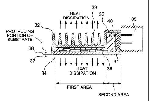
Fig. 1 is a cross section of an electronic
circuit device according to an embodiment of the present
invention. More particularly, the shown electronic
circuit device is applied to a rectifier circuit used in
a motor vehicle or auto-bicycle. The rectifier circuit
receives an AC voltage from a generator and supplies a
DC current to a battery through a bridge formed by
rectifying diodes. The amount of heat generated from
the rectifier circuit is very large. Therefore, heat
dissipation with a high efficiency is required.
In Fig. 1, reference numeral 31 denotes a
metal substrate, numeral 32 denotes a case, numeral 33
denotes a mold resin, numeral 34 denotes a portion of
the case 32 abutting against the substrate 31, numeral
denotes a connector, numeral 36 denotes parts mounted
on a surface of the substrate 31, numeral 37 denotes a
CA 02273474 1999-06-01
- 6 -
surface of the electronic circuit device to be installed
on a pedestal or the like, numeral 38 denotes an end
face of the case 32, numeral 39 denotes a radiating fin
united with the case 32 in one body, and numeral 40
denotes electrodes.
The metal substrate 31 includes a base made of
a metal material such as copper, aluminum or the like
and a conductive pattern of copper or the like formed on
an insulating film of an epoxy resin or the like formed
over the base. The surface mounted parts 36 includes
electronic parts such as rectifying diodes, thyristors
or the like generating a large amount of heat, chip
parts such as transistors, resistors, condensers and so
forth forming a control circuit, jumpers, and so forth.
The electrodes 40 are used for electrically
connecting the electronic circuit device to an external
circuit. The electrode has a height which is at least
two times as high as the surface mounted parts 36. The
connector 35 protects the electrodes 40 and also serves
as a guide for connecting the electrodes 40 to the
external circuit.
The bottom of the case 32 includes a shallow
portion (a first area) in which the low surface mounted
parts 36 are contained and a deep portion (a second
area) in which the high electrodes 40 are contained.
The shallow portion of the case 32 is formed in
proximity to the metal substrate 31 with a first
interval kept therebetween so that satisfactory thermal
CA 02273474 1999-06-01
- 7 -
conduction is attained. The deep portion of the case 32
is formed apart from the metal substrate 31 with a
second interval kept therebetween. The depth ratio of
the deep portion to the shallow portion (that is, the
ratio of the second interval to the first interval) is
at least 2. A space between the metal substrate 31 and
the case 32 is filled with the mold resin 33 for
improving the thermal conduction.
A peripheral portion of the case 32 (excepting
a portion to which the connector 35 is attached) is
provided with a guide for positionally fixing the
metal substrate 31, thereby preventing the positional
deviation of the metal substrate 31 and providing
satisfactory thermal conduction between the metal
substrate 31 and the case 32. Also, the metal substrate
31 is fixed to the substrate abutting portion 34 of the
case 32 so that a part of the metal substrate 31
protrudes from the case 32, thereby providing satis-
factory thermal conduction between the metal substrate
31 and a surface on which the electronic circuit device
is to be installed.
Fig. 2 shows a bottom view of each of the case
32 and the metal substrate 31 used in the electronic
circuit device according to the present embodiment. The
bottom 42 of the case 32 is divided into a shallow area
(the first area) and a deep area (the second area) which
have a difference in level therebetween. As mentioned
above, a peripheral portion (a third area) of the case
CA 02273474 1999-06-01
- 8 -
32 (excepting a portion to which the connector is
attached) is provided with a guide 41 for fixing the
metal substrate 31. Each of the case 32 and the metal
substrate 31 is provided with two mounting holes 43 and
44 or 45 and 46 for fixing the case 32 or the metal
substrate 31, and the case 32 and the metal substrate 31
are brought into close contact with each other at a
portion of the case bottom 42 surrounding the hole (or a
third area). With this structure, not only thermal
conduction but also mechanical strength are improved.
Fig. 3 shows a bottom view and a side view of
the electronic circuit device of the present embodiment
after the completion thereof. As mentioned above, a
part of the metal substrate 31 protrudes from the case
32, thereby providing satisfactory thermal conduction
between the metal substrate 31 and a surface to which
the electronic circuit device is to be attached.
A process for fabrication of the electronic
circuit device according to the present embodiment will
now be described. First, electronic parts such as parts
36, electrodes 40 and so forth are jointed onto a
conductor pattern of a metal substrate 31 by solder.
Next, the metal substrate 31 is fixed to a substrate
abutting portion 34 of a case 32 so that a surface of
the metal substrate 31 having the electronic parts
mounted thereon faces to the case 32. Thereafter, a
mold resin 33 is injected into a space between the metal
substrate 31 and the case 32 from an opening for
CA 02273474 1999-06-01
- 9 -
attachment of a connector 35. The connector 35 is
attached before the mold resin 33 is cured. Since the
fixing of the connector 35 is effected by the mold resin
33, the device is completed if the curing of the mold
resin 33 is completed.
According to the present invention, since heat
dissipation is made from both the radiating fin of the
case and the surface of the metal substrate having no
parts, it is possible to provide an electronic circuit
device which has a heat dissipating efficiency improved
as compared with that of the conventional electronic
circuit device and has a size reduced as a whole.
Further, it is possible to fix the substrate satis-
factorily. As a result, thermal conduction between the
substrate and the case can be improved. The present
invention is remarkably effective when it is particu-
larly applied to an electronic circuit device such as a
rectifier circuit device for a motor vehicle or
motorcycle, that is, in the case where a surface on
which the electronic circuit device is to be installed
is made of a metal so that heat dissipation from that
surface can be expected. Thereby, it is possible to
provide a small-size and high-reliability electronic
circuit device. Accordingly, the present invention has
a large value in industrial use.