Sélection de la langue

Search

Sommaire du brevet 2273474 

Énoncé de désistement de responsabilité concernant l'information provenant de tiers

Une partie des informations de ce site Web a été fournie par des sources externes. Le gouvernement du Canada n'assume aucune responsabilité concernant la précision, l'actualité ou la fiabilité des informations fournies par les sources externes. Les utilisateurs qui désirent employer cette information devraient consulter directement la source des informations. Le contenu fourni par les sources externes n'est pas assujetti aux exigences sur les langues officielles, la protection des renseignements personnels et l'accessibilité.

Disponibilité de l'Abrégé et des Revendications

L'apparition de différences dans le texte et l'image des Revendications et de l'Abrégé dépend du moment auquel le document est publié. Les textes des Revendications et de l'Abrégé sont affichés :

  • lorsque la demande peut être examinée par le public;
  • lorsque le brevet est émis (délivrance).
(12) Brevet: (11) CA 2273474
(54) Titre français: DISPOSITIF POUR CIRCUIT ELECTRONIQUE ET SA METHODE DE FABRICATION
(54) Titre anglais: ELECTRONIC CIRCUIT DEVICE AND METHOD OF FABRICATING THE SAME
Statut: Périmé
Données bibliographiques
(51) Classification internationale des brevets (CIB):
  • H01L 23/34 (2006.01)
  • H01L 23/14 (2006.01)
  • H01L 23/367 (2006.01)
  • H01L 23/42 (2006.01)
  • H01L 25/07 (2006.01)
  • H05K 5/00 (2006.01)
  • H05K 7/20 (2006.01)
(72) Inventeurs :
  • OKAMOTO, MIKIO (Japon)
  • EBARA, KATSUMI (Japon)
(73) Titulaires :
  • SHINDENGEN ELECTRIC MANUFACTURING CO., LTD. (Japon)
(71) Demandeurs :
  • SHINDENGEN ELECTRIC MANUFACTURING CO., LTD. (Japon)
  • HONDA GIKEN KOGYO KABUSHIKI KAISHA (Japon)
(74) Agent: GOWLING WLG (CANADA) LLP
(74) Co-agent:
(45) Délivré: 2008-09-09
(22) Date de dépôt: 1999-06-01
(41) Mise à la disponibilité du public: 1999-12-12
Requête d'examen: 2003-11-17
Licence disponible: S.O.
(25) Langue des documents déposés: Anglais

Traité de coopération en matière de brevets (PCT): Non

(30) Données de priorité de la demande:
Numéro de la demande Pays / territoire Date
10-164987 Japon 1998-06-12

Abrégés

Abrégé français

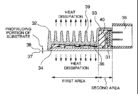
Un dispositif pour circuit électronique doté d'un effet amélioré de dissipation de chaleur, d'une taille compacte et hautement fiable est présenté avec un substrat en métal comportant deux surfaces et un boîtier. Les pièces électroniques sont montées uniquement sur la première surface et le boîtier constitue une structure unique avec une ailette de radiateur. Le substrat en métal est inséré dans le boîtier auquel il sert de capot et la première surface du substrat en métal fait face au boîtier. Une résine est fournie pour remplir un espace entre le substrat en métal et le boîtier, la chaleur générée par les pièces électroniques étant dissipée vers l'extérieur à partir de l'ailette de radiateur et de la seconde surface du substrat en métal.


Abrégé anglais

An electronic circuit device having an improved heat dissipating effect, a small size and a high reliability is provided with a metal substrate having a first surface and a second surface and a case. Electronic parts are mounted on only the first surface and the case is united with a radiating fin in one body. The metal substrate is installed in the case such that the metal substrate serves as a cap of the case and the first surface of the metal substrate faces to the case. A resin is provided to fill up a space between the metal substrate and the case, whereby heat generated from the electronic parts is dissipated to the exterior from both the radiating fin and the second surface of the metal substrate.

Revendications

Note : Les revendications sont présentées dans la langue officielle dans laquelle elles ont été soumises.


-10-

What is claimed is:


1. An electronic circuit device comprising:
a metal substrate having a first surface and a second surface;
electronic parts mounted on only the first surface of said metal substrate;
a case including a radiating fin which is of a one-piece structure therewith,
said case
having said metal substrate housed therein, wherein said metal substrate
serves as a cap of
said case, and the first surface of said metal substrate faces an interior
region of said case; and
a resin disposed in a space between said metal substrate and said interior
region of said
case,
wherein both said radiating fin and the second surface of said metal substrate
dissipate
heat generated from said electronic parts to an exterior of said case, and
wherein said case defines a first area at which said case is distanced from
said metal
substrate with a first interval therebetween providing a least amount of space
needed for
enclosing said electronic parts, and a second area at which said case is
distanced from said
metal substrate with a second interval therebetween, said first interval being
smaller than said
second interval.


2. An electronic circuit device according to claim 1, wherein said case
further defines a third
area at which said case is brought into close contact with said metal
substrate.


3. An electronic circuit device according to claim 2, wherein said first
interval is not larger
than one half of said second interval.


4. An electronic circuit device according to claim 3, wherein said metal
substrate has a
conductive pattern formed on an insulating film formed over a metal plate, and
said electronic
parts includes flat package parts mounted on said conductive pattern and in
the first area of
said case and a plurality of electrodes, mounted on said conductive pattern
and in the second
area of said case, for electrically connecting said electronic circuit device
to an external
circuit.


-11-

5. An electronic circuit device according to claim 2, wherein said case and
said metal
substrate have mounting holes for use of fixing said case and said metal
substrate to each
other, said holes being provided in the third area of said case.


6. An electronic circuit device according to claim 1, wherein said second
surface of said metal
substrate protrudes from said case.


7. An electronic circuit device according to claim 1, wherein said case has a
guide for
positionally fixing said metal substrate to prevent the positional deviation
of said metal
substrate, said guide bringing said case into close contact with said metal
substrate along an
outer periphery of said metal substrate.


8. A method of fabricating an electronic circuit device, the method comprising
the steps of:
mounting electronic parts on a metal substrate having a first surface and a
second
surface, said electronic parts being mounted on only the first surface of said
metal substrate,
said electronic parts including a plurality of electrodes for connecting said
electronic circuit
device to an external circuit;
installing said metal substrate in a case including a radiating fin which is
of a one-
piece structure therewith, wherein said metal substrate serves as a cap of
said case and the
first surface of said metal substrate faces an interior region of said case,
said case being
provided with an opening for drawing out said plurality of electrodes to an
exterior;
injecting laterally a resin into said interior region between said metal
substrate and
said case from said opening of said case; and
inserting a member into said opening of said case to protect said plurality of

electrodes.


9. An electronic circuit device according to claim 1, wherein said radiating
fin is located at
said first area of said case.

Description

Note : Les descriptions sont présentées dans la langue officielle dans laquelle elles ont été soumises.


CA 02273474 2007-06-19

1
ELECTRONIC CIRCUIT DEVICE AND METHOD OF FABRICATING
THE SAME

BACKGROUND OF THE INVENTION
Field of the Invention

The present invention relates to an electronic
circuit device for which a high heat radiating or
dissipating ability is required and a method of
fabricating such an electronic circuit device, and more
particularly to the structure of a package of an
electronic circuit device and a method for fabrication of
the same.

Description of Related Art

Prior art will be described referring to FIGS. 4 and
5.

FIG. 4 shows the setting structure of a rectifier
for vehicle disclosed by Japanese Utility Model
Publication No. 6-9577 published on March 9, 1994. A
frame member 16 and a substrate 12 are fixed through
screws 20 onto a surface of a pedestal or the like (not
shown) on which the rectifier is to be installed.
Thereby, a structure having an excellent productivity and
a satisfactory heat dissipating efficiency is provided.
In this structure, no radiating fin is used. There
instead, heat dissipation is mainly made from a surface
of the rectifier to be installed on the pedestal or the
like (or a surface of the substrate 12 having no parts
mounted thereon).


CA 02273474 1999-06-01

- 2 -

On the other hand, the conventional electronic
circuit device using a radiating fin is shown in Fig. 5.
In the figure, reference numeral 21 denotes a metal
substrate, numeral 22 denotes a case, numeral 23 denotes

a mold resin, numeral 24 denotes a portion of the case
22 abutting against the substrate 21, numeral 25 denotes
a connector, numeral 27 denotes an installation surface
of the electronic circuit device, numeral 28 denotes an
end face of the case 22, and numeral 29 denotes a

radiating fin. In such conventional electronic circuit
device with radiating fin, a surface of the metal
substrate having no parts mounted thereon is brought
into contact with the bottom of the case, thereby
improving the heat dissipation from the radiating fin.

However, in the setting structure of the
rectifier for vehicle shown in Fig. 4, heat dissipation
is mainly made from the surface of the substrate 12
having no parts mounted thereon, that is, the heat
dissipation from a surface of the substrate having parts

mounted thereon is not taken into consideration.

In the electronic circuit device shown in Fig.
5, the dissipation of heat thermally conducted from the
surface of the metal substrate 21 having no parts
mounted thereon and radiated from the radiating fin 29

is satisfactory but the heat dissipation from the
installation surface of the electronic circuit device
(or a surface of the metal substrate 21 having parts
mounted thereon) is not particularly taken into


CA 02273474 1999-06-01

- 3 -
consideration.

SUMMARY OF THE INVENTION

An object of the present invention made in
light of the above-mentioned problems is to provide an
electronic circuit device which has a heat dissipating

ability superior to that of the conventional device.
To attain the above object, an electronic
circuit device according to the present invention
comprises a metal substrate having a first surface and a

second surface, electronic parts mounted on only the
first surface of the metal substrate, a case, united
with a radiating fin in one body, for housing the metal
substrate therein such that the metal substrate serves
as a cap of the case and the first surface of the metal

substrate faces to the case, and a resin disposed in a
space between the metal substrate and the case, whereby
heat generated from the electronic parts is dissipated
to the exterior from both the radiating fin and the

second surface of the metal substrate.

A method of fabricating an electronic circuit
device according to the present invention comprises the
step of mounting electronic parts on a metal substrate
having a first surface and a second surface, the

electronic parts being mounted on only the first surface
of the metal substrate, the electronic parts including a
plurality of electrodes for connecting the electronic
circuit device to an external circuit, the step of


CA 02273474 1999-06-01

- 4 -

installing the metal substrate in a case united with a
radiating fin in one body such that the metal substrate
serves as a cap of the case and the first surface of the
metal substrate faces to the case, the case being

provided with an opening for drawing out the plurality
of electrodes to the exterior, the step of injecting a
resin into a space between the metal substrate and the
case from the opening of the case, and the step of

inserting a member into the opening of the case which
protects the plurality of electrodes.

With the construction of the present invention
in which the metal substrate is installed in the case
such that the metal substrate serves as a cap of the
case and the surface of the metal substrate having the

parts mounted thereon faces to the case or a surface of
the metal substrate having no parts is directed outwards
and the space between the metal substrate and the case
is filled with the resin, a large amount of heat can be
dissipated from both the radiating fin of the case and a

surface of the electronic circuit device to be installed
on a pedestal or the like, that is, a surface of the
metal substrate having no parts, thereby improving the
heat dissipation of the metal substrate.

BRIEF DESCRIPTION OF THE DRAWINGS

Fig. 1 is a cross section of an electronic
circuit device according to an embodiment of the present
invention;


CA 02273474 1999-06-01

- 5 -

Fig. 2 is a bottom view of each of a case and
a metal substrate used in the electronic circuit device
according to the embodiment of the present invention;

Fig. 3 is a bottom view and a side view of the
electronic circuit device according to the embodiment of
the present invention;

Fig. 4 is an assembly diagram of one conven-
tional electronic circuit device; and

Fig. 5 is a cross section of another conven-
tional electronic circuit device.

DETAILED DESCRIPTION OF THE EMBODIMENTS

Fig. 1 is a cross section of an electronic
circuit device according to an embodiment of the present
invention. More particularly, the shown electronic

circuit device is applied to a rectifier circuit used in
a motor vehicle or auto-bicycle. The rectifier circuit
receives an AC voltage from a generator and supplies a
DC current to a battery through a bridge formed by

rectifying diodes. The amount of heat generated from
the rectifier circuit is very large. Therefore, heat
dissipation with a high efficiency is required.

In Fig. 1, reference numeral 31 denotes a
metal substrate, numeral 32 denotes a case, numeral 33
denotes a mold resin, numeral 34 denotes a portion of

the case 32 abutting against the substrate 31, numeral
denotes a connector, numeral 36 denotes parts mounted
on a surface of the substrate 31, numeral 37 denotes a


CA 02273474 1999-06-01

- 6 -

surface of the electronic circuit device to be installed
on a pedestal or the like, numeral 38 denotes an end
face of the case 32, numeral 39 denotes a radiating fin
united with the case 32 in one body, and numeral 40

denotes electrodes.

The metal substrate 31 includes a base made of
a metal material such as copper, aluminum or the like
and a conductive pattern of copper or the like formed on
an insulating film of an epoxy resin or the like formed

over the base. The surface mounted parts 36 includes
electronic parts such as rectifying diodes, thyristors
or the like generating a large amount of heat, chip
parts such as transistors, resistors, condensers and so
forth forming a control circuit, jumpers, and so forth.

The electrodes 40 are used for electrically
connecting the electronic circuit device to an external
circuit. The electrode has a height which is at least
two times as high as the surface mounted parts 36. The
connector 35 protects the electrodes 40 and also serves
as a guide for connecting the electrodes 40 to the

external circuit.

The bottom of the case 32 includes a shallow
portion (a first area) in which the low surface mounted
parts 36 are contained and a deep portion (a second

area) in which the high electrodes 40 are contained.
The shallow portion of the case 32 is formed in
proximity to the metal substrate 31 with a first
interval kept therebetween so that satisfactory thermal


CA 02273474 1999-06-01
- 7 -

conduction is attained. The deep portion of the case 32
is formed apart from the metal substrate 31 with a
second interval kept therebetween. The depth ratio of
the deep portion to the shallow portion (that is, the

ratio of the second interval to the first interval) is
at least 2. A space between the metal substrate 31 and
the case 32 is filled with the mold resin 33 for
improving the thermal conduction.

A peripheral portion of the case 32 (excepting
a portion to which the connector 35 is attached) is
provided with a guide for positionally fixing the

metal substrate 31, thereby preventing the positional
deviation of the metal substrate 31 and providing
satisfactory thermal conduction between the metal

substrate 31 and the case 32. Also, the metal substrate
31 is fixed to the substrate abutting portion 34 of the
case 32 so that a part of the metal substrate 31
protrudes from the case 32, thereby providing satis-
factory thermal conduction between the metal substrate

31 and a surface on which the electronic circuit device
is to be installed.

Fig. 2 shows a bottom view of each of the case
32 and the metal substrate 31 used in the electronic
circuit device according to the present embodiment. The

bottom 42 of the case 32 is divided into a shallow area
(the first area) and a deep area (the second area) which
have a difference in level therebetween. As mentioned
above, a peripheral portion (a third area) of the case


CA 02273474 1999-06-01

- 8 -

32 (excepting a portion to which the connector is
attached) is provided with a guide 41 for fixing the
metal substrate 31. Each of the case 32 and the metal
substrate 31 is provided with two mounting holes 43 and

44 or 45 and 46 for fixing the case 32 or the metal
substrate 31, and the case 32 and the metal substrate 31
are brought into close contact with each other at a
portion of the case bottom 42 surrounding the hole (or a
third area). With this structure, not only thermal

conduction but also mechanical strength are improved.
Fig. 3 shows a bottom view and a side view of
the electronic circuit device of the present embodiment
after the completion thereof. As mentioned above, a
part of the metal substrate 31 protrudes from the case

32, thereby providing satisfactory thermal conduction
between the metal substrate 31 and a surface to which
the electronic circuit device is to be attached.

A process for fabrication of the electronic
circuit device according to the present embodiment will
now be described. First, electronic parts such as parts
36, electrodes 40 and so forth are jointed onto a

conductor pattern of a metal substrate 31 by solder.
Next, the metal substrate 31 is fixed to a substrate
abutting portion 34 of a case 32 so that a surface of

the metal substrate 31 having the electronic parts
mounted thereon faces to the case 32. Thereafter, a
mold resin 33 is injected into a space between the metal
substrate 31 and the case 32 from an opening for


CA 02273474 1999-06-01

- 9 -

attachment of a connector 35. The connector 35 is
attached before the mold resin 33 is cured. Since the
fixing of the connector 35 is effected by the mold resin
33, the device is completed if the curing of the mold

resin 33 is completed.

According to the present invention, since heat
dissipation is made from both the radiating fin of the
case and the surface of the metal substrate having no
parts, it is possible to provide an electronic circuit

device which has a heat dissipating efficiency improved
as compared with that of the conventional electronic
circuit device and has a size reduced as a whole.
Further, it is possible to fix the substrate satis-
factorily. As a result, thermal conduction between the

substrate and the case can be improved. The present
invention is remarkably effective when it is particu-
larly applied to an electronic circuit device such as a
rectifier circuit device for a motor vehicle or
motorcycle, that is, in the case where a surface on

which the electronic circuit device is to be installed
is made of a metal so that heat dissipation from that
surface can be expected. Thereby, it is possible to
provide a small-size and high-reliability electronic
circuit device. Accordingly, the present invention has

a large value in industrial use.

Dessin représentatif
Une figure unique qui représente un dessin illustrant l'invention.
États administratifs

Pour une meilleure compréhension de l'état de la demande ou brevet qui figure sur cette page, la rubrique Mise en garde , et les descriptions de Brevet , États administratifs , Taxes périodiques et Historique des paiements devraient être consultées.

États administratifs

Titre Date
Date de délivrance prévu 2008-09-09
(22) Dépôt 1999-06-01
(41) Mise à la disponibilité du public 1999-12-12
Requête d'examen 2003-11-17
(45) Délivré 2008-09-09
Expiré 2019-06-03

Historique d'abandonnement

Il n'y a pas d'historique d'abandonnement

Historique des paiements

Type de taxes Anniversaire Échéance Montant payé Date payée
Enregistrement de documents 100,00 $ 1999-06-01
Le dépôt d'une demande de brevet 300,00 $ 1999-06-01
Taxe de maintien en état - Demande - nouvelle loi 2 2001-06-01 100,00 $ 2001-04-17
Taxe de maintien en état - Demande - nouvelle loi 3 2002-06-03 100,00 $ 2002-04-11
Taxe de maintien en état - Demande - nouvelle loi 4 2003-06-02 100,00 $ 2003-04-10
Requête d'examen 400,00 $ 2003-11-17
Taxe de maintien en état - Demande - nouvelle loi 5 2004-06-01 200,00 $ 2004-04-07
Taxe de maintien en état - Demande - nouvelle loi 6 2005-06-01 200,00 $ 2005-04-13
Taxe de maintien en état - Demande - nouvelle loi 7 2006-06-01 200,00 $ 2006-04-18
Taxe de maintien en état - Demande - nouvelle loi 8 2007-06-01 200,00 $ 2007-04-16
Taxe de maintien en état - Demande - nouvelle loi 9 2008-06-02 200,00 $ 2008-04-14
Taxe finale 300,00 $ 2008-06-16
Taxe de maintien en état - brevet - nouvelle loi 10 2009-06-01 250,00 $ 2009-04-20
Taxe de maintien en état - brevet - nouvelle loi 11 2010-06-01 250,00 $ 2010-04-14
Taxe de maintien en état - brevet - nouvelle loi 12 2011-06-01 250,00 $ 2011-04-08
Enregistrement de documents 100,00 $ 2011-11-03
Taxe de maintien en état - brevet - nouvelle loi 13 2012-06-01 250,00 $ 2012-04-23
Taxe de maintien en état - brevet - nouvelle loi 14 2013-06-03 250,00 $ 2013-04-04
Taxe de maintien en état - brevet - nouvelle loi 15 2014-06-02 450,00 $ 2014-04-02
Taxe de maintien en état - brevet - nouvelle loi 16 2015-06-01 450,00 $ 2015-04-29
Taxe de maintien en état - brevet - nouvelle loi 17 2016-06-01 450,00 $ 2016-05-05
Taxe de maintien en état - brevet - nouvelle loi 18 2017-06-01 450,00 $ 2017-05-05
Taxe de maintien en état - brevet - nouvelle loi 19 2018-06-01 450,00 $ 2018-05-02
Titulaires au dossier

Les titulaires actuels et antérieures au dossier sont affichés en ordre alphabétique.

Titulaires actuels au dossier
SHINDENGEN ELECTRIC MANUFACTURING CO., LTD.
Titulaires antérieures au dossier
EBARA, KATSUMI
HONDA GIKEN KOGYO KABUSHIKI KAISHA
OKAMOTO, MIKIO
Les propriétaires antérieurs qui ne figurent pas dans la liste des « Propriétaires au dossier » apparaîtront dans d'autres documents au dossier.
Documents

Pour visionner les fichiers sélectionnés, entrer le code reCAPTCHA :


Pour visualiser une image, cliquer sur un lien dans la colonne description du document. Pour télécharger l'image (les images), cliquer l'une ou plusieurs cases à cocher dans la première colonne et ensuite cliquer sur le bouton "Télécharger sélection en format PDF (archive Zip)" ou le bouton "Télécharger sélection (en un fichier PDF fusionné)".

Liste des documents de brevet publiés et non publiés sur la BDBC .

Si vous avez des difficultés à accéder au contenu, veuillez communiquer avec le Centre de services à la clientèle au 1-866-997-1936, ou envoyer un courriel au Centre de service à la clientèle de l'OPIC.


Description du
Document 
Date
(yyyy-mm-dd) 
Nombre de pages   Taille de l'image (Ko) 
Abrégé 1999-06-01 1 22
Description 2007-06-19 9 335
Revendications 2007-06-19 2 87
Dessins représentatifs 1999-11-24 1 10
Description 1999-06-01 9 334
Revendications 1999-06-01 3 92
Dessins 1999-06-01 3 81
Page couverture 1999-11-24 1 39
Dessins représentatifs 2008-08-22 1 14
Page couverture 2008-08-22 1 47
Poursuite-Amendment 2007-06-19 8 278
Taxes 2005-04-13 1 30
Poursuite-Amendment 2003-11-17 1 35
Cession 1999-06-01 3 128
Taxes 2003-04-10 1 35
Poursuite-Amendment 2004-01-27 1 32
Taxes 2001-04-17 1 30
Taxes 2002-04-11 1 34
Taxes 2004-04-07 1 33
Taxes 2006-04-18 1 45
Poursuite-Amendment 2006-12-27 2 63
Taxes 2007-04-16 1 42
Correspondance 2008-06-16 2 51
Taxes 2008-04-14 1 42
Taxes 2009-04-20 1 34
Taxes 2010-04-14 1 38
Cession 2011-11-03 4 140