Note: Descriptions are shown in the official language in which they were submitted.
1
Solar Module
The present invention relates to a solar module according to the introductory
part
of the claim 1.
A solar module is known e.g. from EP-A-0 525 225 which is based on a glass sub-
strate consisting of hardened solar glass of 4 mm thickness. Onto the glass
sub-
strate a stack of layers is laminated consisting of a first synthetic film,
electrically
interconnected solar cells, a second synthetic film and a composite film as a
cover
film. Laminating is effected under vacuum at an elevated temperature in which
process the synthetic films are welded onto each other and forming a solid com-
pound with the substrate.
Furthermore from DE-41 28 766 a solar module is known comprising a number of
solar cells interconnected into a solar cell string in which arrangement a
transpar-
ent substrate pane is provided with a screen printed conductor system. The
rear
contacts of the solar cells in this arrangement contact the screen
print.conductor
system within a solar cell string. The front contacts of the solar cells
within a solar
cell string are connected in parallel or in series mutually andlor to the rear
contacts
of neighbouring solar cells if required. A transparent cover pane is connected
to
the substrate pane, in the manner of a composite safety glass, using a
connecting
compound e.g. on basis of a plastic film or a cast resin. The cover pane also
is
provided with a screen printed conductor system which within a solar cell
string
contacts the front contacts of the solar cells in such a manner that front
and/or rear
contacts of neighbouring solar cells are electrically interconnected.
In a further design example according to Fig. 4 of the cited document the
cover
pane and the substrate pane form the individual panes of an insulating glass
pane
in which arrangement the solar cells are located in the air-filled interspace
be-
tween the panes. The panes in this arrangement are spaced at the required dis-
tance -using spacers. Between the solar cell strings and the screen printed
con-
ductor systems of the cover pane and of the substrate pane electrically
conducting
KGSp001
CA 02360814 2001-07-17
2
hook-shaped or U-shaped spacer elements are arranged in such a manner that
the solar cell strings are soldered to the screen print conductor systems not
di-
rectly but via the spacer elements. Obviously this design example is of
secondary
importance only as in the patent claims only a solar module with a connecting
compound based on a plastic film or on a cast resin is referred to, i.e. the
inter-
space is filled with a cast resin mass according to the examples described
with
reference to the Figures 1 through 3.
The example according to Fig. 4 of the patent document cited above will hardly
be
economically feasible for various reasons as even small tensions differences
between cover and substrate panes may cause glass breakages of the solar
modules. Further the screen print conductor systems applied to both sides of
the
solar module impair the effectiveness of the solar irradiation which may cause
considerable power loss. Due to the wiring of the solar cells on alternating
faces a
relatively high resistance is generated which further reduces the yield.
The known solar modules in which the solar cells are embedded in a synthetic
film
or in a cast resin mass are hardly suitable for recycling, since separation
and
elimination of glass substrates, synthetic films and/or cast resins and
conductors
being very demanding and thus so expensive that elimination of the elements as
hazardous waste rather proves economically feasible.
It thus is the objective of the present invention to improve a solar module as
men-
tioned above in such a manner that a particularly simple arrangement results
and
that the solar modules in case of glass breakage or similar damages can be
recy-
cled, or re-used respectively, without difficulties.
This objective is met using a solar module presenting the characteristics
according
to the patent claim 1.
The inventive solar module presents the important advantage that the
individual
solar cells held therein can be exchanged in relatively simple manner, and
that the
KGSp001
CA 02360814 2001-07-17
3
solar cells still are very effectively protected against weather exposure such
as
solar irradiation, rain and similar influences. Tensions generated in the
glass sub-
strates due to such influences, owing to the unilateral connection of the
solar cells
to one glass substrate only, are not transmitted, or are transmitted to an
insignifi-
cant degree merely, to the solar cells. Owing to the simple lay-out of the
inventive
solar module also the energy spent in manufacturing the module is considerably
lower compared to conventional modules, and thus manufacturing cost can be
lowered by one third or more.
Further advantages of the present invention are explained in the dependent
patent
claims and in the following description in which the present invention is
discussed
in more detail with reference to a design example illustrated in schematic
draw-
ings. It is shown in:
Fig. 1 a schematic view of the lay-out of a solar module seen in a top view,
Fig. 2 a section of the solar module along the line A-A according to Fig. 1,
Fig. 3 a first arrangement of the conductors on the glass substrate, and
Fig. 4 a second arrangement of the conductors.
In the Figures identical elements are referred to using the same reference
signs,
and explanations given first are valid unless stated otherwise specifically.
In Fig. 1 a top view of a solar module 1 is shown in purely schematic manner,
with
a support pane 2 laid out as a glass substrate and a congruent cover pane 3
laid
out as a glass substrate, the two panes being spaced by a predetermined
distance
using a sealing spacer frame 4 indicated with dashed lines arranged at their
bor-
der zones. The glass substrate 2 is provided with conductor leads 6 to which
the
solar cells 7 are connected via soldered bridges. The conductors 6 are
provided
with contacting leads 8 and 9 extending to the outside and laid out as
positive
KGSp001
CA 02360814 2001-07-17
4
ports, and negative ports respectively. The solar-cells 7 as such can be known
silicon or titanium cells, or photochemical cells respectively, as described
e.g. in
EP-B-0 525 070.
In Fig. 2 part of the cross-section along the line A-A according to Fig. 1 of
the solar
module 1 is shown. The solar cells 7 are fastened unilaterally to the
conductor
leads 6 on the support pane 2 using soldering bridges 10 at a distance from
the
two glass substrates 2 and 3. Additional elastic fastening elements such as
bind-
ing spots formed by a silicon adhesive also can be provided which are not
shown
further here. The solar cells 7 thus are arranged more or less freely in the
air-filled
interspace 11 between the two glass substrates 2 and 3. The support pane 2 as
well as the cover pane 3 are made from a silicate glass, preferentially a
colourless
(white) glass, of a thickness of less than 5 mm. Depending on the application
de-
sired also a certain silicate quantity of recycled glass maybe used for
manufactur-
ing the glass substrates 2 and 3. On the inner faces of both substrates 2 and
3 a
thin layer 12 and 13 each of a light reflecting paint presenting a light
reflectance
value of more than 62% is applied. This paint advantageously is a ceramic
paint,
also known as so-called glass pastes. For this purpose the ceramic paint is ap-
plied to the glass substrates using the screen print method and in a tunnel
kiln is
baked onto the surface at a temperature exceeding 600 °C. Also the
conductors 7
are printed onto the glass substrate 2 using an electrically conductive paste,
pref-
erentially a silver paste, and are baked in at a temperature exceeding 600
°C.
Baking of the ceramic paint and of the electrically conductive paste can be ef-
fected in the same processing step. Instead of applying a ceramic paint coat
the
glass substrates 2 and 3 also can be subject to a surface treatment such as
sand
blasting or chemical etching in such a manner that on their outer surfaces
they are
rendered non-reflecting with a high diffusion effect. Other types of non-
reflecting
glass also can be applied for manufacturing the glass substrates 2 and 3. In
order
to equalise tensions in the glass substrates 2 and 3, the dimension of which
can
be e.g. 100 cm by 100 cm, the glass substrates are thermally pre-stressed,
i.e.
they are heated in a tunnel kiln on rolls to a temperature. of about 600
°C to 700 °C
and then are shock-chilled in a cold air stream.
KGSp001
CA 02360814 2001-07-17
5
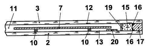
The spacer frame 4 furthermore contains a glass rod of rectangular cross-
section
serving as a spacer element, the thickness of which is chosen between about 6
and 16 mm, preferentially at about 8 mm. In the outer corners of the glass rod
15
formed with the glass substrates 2 and 3 a seal 16 is provided made from butyl
rubber. On the outer side of the glass spacer 15 then a further seal 17 is
provided
made from a rubber-elastic material such as silicon rubber, or e.g. a melt
adhesive
known under the trade mark "Bynel" or "hot melt", acting as a water moisture
bar-
rier for the solar module 1. However, seal 16 could be omitted and only seal
17
could be provided. The spacer 15 also can be made from other materials, e.g.
from wooden slats of a hard wood, such as oak or beech wood. Also aluminium
slats can be provided which are fastened between the glass substrates 2 and 3
using a melt adhesive ("hot melt"). Inside the solar module 1 furthermore a mo-
lecular sieve 19 can be provided as a drying agent such as e.g. zeolite in
order to
reduce the residual humidity within the interspace 11 and to protect the solar
cells
6 against corrosion. Additionally a humidity gauge 20 can be arranged in the
inter-
space 11 between the glass substrates 2 and 3, of which the electric contacts
of
which also can be extended to the outside via conductor leads which are not
shown here. Using this arrangement humidity inside a solar module 1 can be
monitored and any leaks in the solar module 1 can be detected.
In Fig. 4 an arrangement of a number of parallel conductor leads 6 is shown in
the
sense of an example each of which is soldered to an oblong solar cell 7 (shown
with dashed lines). In the manufacturing process one single large silicon
board is
soldered onto the conductor leads 6 and subsequently the board is cut, using a
laser beam, into the individual oblong solar cells 7. To the left and the
right of the
glass substrate or of the support pane 2 the two connecting ports (positive
and
negative) are indicated. In Fig. 4 a further arrangement of the conductor
leads 6 is
shown provided for the four solar cells 7 indicated with dashed lines.
It furthermore is feasible to mount the support pane 2 and the cover pane 3
not
exactly congruent above each other using the spacer frame 4 but slightly
offset. In
KGSp001
CA 02360814 2001-07-17
6
this manner a plurality of solar modules 1 can be lined up seamlessly the ar-
rangement forming a larger array. The solar modules lined up in this manner
can
form a wall, or a so-called weather coat for building facades, respectively,
on roofs
or similar parts of a building.
It has been proven that the energy consumed in manufacturing the inventive
solar
module 1 is in the order of 30 to 50 kWh per m2 the glass substrate
thicknesses
being chosen between 3.5 and 4.5 mm. This corresponds to about 2.2 kWh per kg
of glass.
KGSp001
CA 02360814 2001-07-17