Note: Descriptions are shown in the official language in which they were submitted.
CA 02397857 2010-12-07
OLED DEVICES WITH PHOTORESIST MASK/SMOOTHING LAYER
FIELD OF THE INVENTION
The invention relates to the field of optical devices, and in particular to
organic light
emitting devices (OLEDs), and to a method of manufacturing such devices.
BACKGROUND OF THE INVENTION
OLEDs have recently shown promise for use as a light source in optical
displays. A
typical structure for an OLED is shown in Figure 1 and consists of a stack of
organic
semiconductor layers 10 between a transparent electrode 12 (usually an indium
tin oxide
(ITO) layer acting as an anode) on a glass substrate 14 and another
electrode16 (usually a
layer of low work function metal, metal alloy or cermet material acting as a
cathode). At
positive bias, electric current will flow through the device and light
emission will occur
between the overlapped area of anode and cathode.
In order to display information, it is necessary to make pixels of the
required shape. This
can be achieved either by patterning the first electrode (anode) or using
shadow masks to
define the shape of the second electrode, or patterning both electrodes
depending on the
application.
The vertical dimension of organic light emitting devices (OLED) is usually
very thin. To
optimize the hole-transport, electron-transport properties and device
efficiency, the total
thickness of the organic layer between the cathode and anode is typically
between 100 nm
and 200 nm. A typical OLED has an electric field of _106V/cm during device
operation.
This high electric field makes OLEDs very sensitive to the edges of patterned
ITO
substrates (the first electrode) or other types of electrode on which the
organic materials is
deposited. Imperfect step coverage of the deposited organic materials will
result in a
substantially higher electric field and higher local current density at that
area. This will
cause the device to break down.
1
CA 02397857 2010-12-07
Figure 2 shows an anode 12 that has been patterned for form three OLED devices
20a,
20b, 20c. The lack of anode material between the devices causes a step between
the
portions of the deposited cathode layer 16a and organic layer l0a located
between the
OLED devices and between the portions of the same layers, 16b, 10b over the
OLED
devices. Figure 2 shows that in some cases the patterned ITO layer 12 or other
type of
electrode layer is thicker than the organic layer 10..Since thermal vacuum
deposition,
which is used to deposit the organic layer 12, is generally non-conformal,
some
uncovered ITO anode area 21 will come into contact with the metal cathode
layer 16
deposited after the deposition of the organic layers 12. This will. cause
massive short
circuits in the devices.
Because of the non-conformal nature of the thermal deposition, when the total
thickness
of ITO anode and organic layers exceeds the thickness of the cathode layer, a
discontinuity 22 may occur in cathode layer where it passes from the OLED to
the area
between the OLEDs. This type of discontinuity will cause device failure in
OLEDs based
on a common cathode (or common anode) design and may also cause device failure
in
individual pixels or segments due to the open circuit between the electrode
layer and
connection pads.
Deposited silicon oxide, aluminum oxide, or silicon nitride is typically used
to define an
emissive area. After the deposition of insulating material, a
photolithographic process and
an etching process are necessary to create pixel areas and sloped edges. Such
a process is
described in U.S. Patent No. 6,069,443. This process is complicated. It
involves dielectric
deposition, a photolithographic process, and at least one etching step for
creating pixel areas.
The deposition of dielectric material is also expensive.
2
CA 02397857 2003-08-13
Various solutions have been proposed in the prior art, all of which are
unsatisfactory for
one reason or another. Mathine et al (U of Arizona) [D.L. Mathine et al, Appl.
Phys.
Lett., 76(26), 2000, p3849], describes the use of PEDOT:PSS (poly(ethylened
ioxythiophene) doped with polystyrenesulfonate) as a buffer layer between a
CMOS
active matrix and the OLED. It is spun-5 on and forms a 20nm thick conformal
layer that
covers the dielectric edges between pixels. It is resistive enough not to
short the different
pixels, and helps charge injection into the hole transport layer. A lift-off
photoresist
pattern is applied prior to PEDOT:PSS so that layer can be lifted off the
connection pads.
The layer is too thin to smooth out underlying structures and is actually part
of the diode.
Shimoda (Seiko, CDT) [Asia Display 98, p2171 use an Si02 "adhesive" layer and
a
polyimide "interval layer" between a TFT active matrix and the PLEDs. Both
have
openings that define the pixels. Shimoda's layer is an insulating and
passivation layer.
The edges are not sloped.
Steward et al (U of Lehigh and Emagin, old FED Corp) [IEDM 98, p871] use two
spin-
on-glass layers for planarization of a TFT matrix. The first layer goes below
the ITO
anode to ensure planarity of the ITO electrode on top of the matrix, and the
second layer
defines pixel openings and smoothes the matrix. The SOG layers are spun, cured
at
300 C, patterned and wet-etched in a certain way so that the organic materials
have good
step coverage.
Jones (Emagin, old FED Corp) [U.S. Patent No 6,069,443] describes the use of a
separator for passive matrix displays with an overhanging profile and an
underlying
insulator that prevents short-circuits from happening when the cathode flows
on top of the
organics edge defined by the overhanging separator. Jones employs an
underlying
3
CA 02397857 2010-12-07
insulator with openings that substantially define pixels, and with tapered
edges to
minimize edge shorts. The purpose of Jones' structure is to prevent short-
circuits.
Smoothing layers have been used in LCDs between the color filters, patterned
first on the
substrate, and the ITO electrode (see for example U.S. Patent No. 5,488,497).
In this case
the goal is to ensure color purity and has nothing to do with field
homogeneity since
liquid crystal layers are very thick compared to the thickness of the
electrodes.
SUMMARY OF THE INVENTION
According to the present invention there is provided a method of making an
organic light
emitting device (OLED) comprising forming a structure with stepped edges;
depositing a
conformal smoothing layer over said structure, said smoothing layer having a
thickness
greater than said structure; patterning said smoothing layer to expose
portions of said
structure underlying said smoothing layer and defining active regions of said
device;
treating said smoothing layer to taper said smoothing layer over said stepped
edges of
said structure on said exposed portions; and depositing additional layers over
said
smoothing layer and said exposed portions of said structure.
In one embodiment the invention provides a photoresist-based smoothing mask
technique
to overcome the difficulties encountered in the prior art in the fabrication
of OLEDs. The
use of a photoresist as a smoothing layer permits direct patterning of the
OLEDs and
simplified sloping by temperature reflow.
In accordance with the principles of the invention the applied smoothing layer
has
openings to define the pixels and blunts all underlying layer edges in order
to ensure that
the thickness of organic layers is as constant as possible everywhere they are
covered by
the top electrode. This arrangement results in a homogeneous field across the
individual
pixels and continuity in the layers. deposited after the photoresist layer.
4
CA 02397857 2003-08-13
A particularly convenient class of material to use for the smoothing layer is
photosensitive resins. Such resins have several advantages. They can be used
in spin
coating and therefore provide a conformal coating smoothing out all edges.
They can be
directly patterned by lithography (exposure and development) without pattern
transfer,
thereby providing a simple process. They reflow during a hard-bake, which in
this case
stabilizes the photoresist and provides a smooth pixel edge. They are of a
similar nature to
the active materials of the OLEDs and therefore will be protected by any
passivation
layers that are applied to ensure the integrity of the OLEDs.
The invention thus relates to a technique which can use commercially available
photoresist as a masking/ smoothing layer to define the emissive and non-
emissive areas
of the light emitting devices. Typical thickness of this layer is in the up to
about 2
microns, for example, 1 - 2 microns, that is thick enough to cover all the
steps produced
after ITO etching. During the baking process, the photoresist reflows,
providing a tapered
slope at the edge. This photoresist layer therefore not only functions as a
mask layer to
define an active area but also blunts the steep edges produced by ITO
patterning and
provides tapered edges to maintain continuity in the cathode layer so that the
device can
be connected to the outside world. Subsequently, organic layers and a metal
cathode are
applied to complete the process. In this way, short circuits and
discontinuities in cathode
can be substantially avoided.
The invention also provides an organic light emitting device comprising a
structure with
stepped edges; a patterned conformal smoothing layer extending over said
structure and
exposing portions of said structure underlying said smoothing layer defining
active
regions of said device, said smoothing layer having a thickness greater than
said structure
and tapering over said stepped edges of said structure on said exposed
portions; and
5
CA 02397857 2010-12-07
additional organic and metal layers over said smoothing layer and said exposed
portions
of said structure.
BRIEF DESCRIPTION OF THE DRAWINGS
The invention will now be described in more detail, by way of example only,
with
reference to the accompanying drawings, in which:
Figure 1 is a schematic illustration of a typical OLED;
Figure 2 is a schematic illustration of a plurality of OLEDs and possible
defects
encountered in such devices;
Figures 3 and 4 illustrate process steps in accordance with one embodiment of
the
invention;
Figure 5 shows a plurality of OLEDs on a wafer made according to one
embodiment of
the invention; and
Figure 6 is a set of graphs showing the characteristics of OLEDs made
according to one
embodiment of the invention.
DETAILED DESCRIPTION OF THE INVENTION
A method of making an OLED in accordance with one embodiment of the invention
will
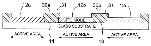
now be described with reference Figures 3 and 4: An ITO coated glass substrate
14 is
cleaned in a conventional manner. The ITO layer 12 is then patterned and
etched to
produce individual anodes 12a, 12b, 12c. It will be appreciated that other
suitable
transparent materials can be employed for the substrate.
A layer of commercial photoresist 30 approximately up to approximately 2 tm
thick is
applied between the individual anodes. This layer is exposed and developed to
leave the
individual columns 30a, 30b of photoresist protruding between the individual
anodes and
overhanging slightly over the step edges 31 of the anodes 12.
6
CA 02397857 2003-08-13
The wafer is then subjected to a baking step in which the photoresist reflows
to produce
columns with tapered edges 32 overhanging the exposed portions of the
individual anodes
as shown in Figure 4.
The photoresist layer acts as a mask for the subsequent deposition by thermal
evaporation
of the organic layer 10 and the metal cathode layer 16. As will be seen in
Figure 5, these
two layers 10, 16 smoothly follow the contour of the photoresist layer 30 and
as result
steps, which might cause short-circuits, and sharp discontinuities are
avoided. No short
circuits are formed in the regions 23, 24, and no discontinuity is present in
region 25.
Figure 6 shows the characteristics of OLEDs made using the above process. The
devices
were made of a multi-layer organic stack on an ITO (120 rim) anode. The
organic stack
consisted of CuPc(5nm)NPB(30nm)/NPB:Rubrene(100:1, 40 nm) /A1g3(40nm). The
chemical structure of the compounds is as follows:
,I A1q3
KN.
3
NPB
7
CA 02397857 2003-08-13
Rubrene
N
N
CuPc
The metal cathode 16 consisted of a layer of Ag(60nm) and a layer of an Mg:Ag
alloy
(10:1, 100nm).
As can be seen in the graphs shown in Figure 6, these devices show very good
characteristics with respect to current-voltage and luminance properties
compared to
devices made without the smoothing layer. The photoresist smoothing layer
blunts all
underlying layer edges and provides sloped edge wherever a step occurs from
one layer to
another. This process ensures the thickness of the organic layers as constant
as possible
everywhere they are covered by the top electrode, thus the use of a smoothing
layer
results in a homogeneous field across the pixel.
The use of a photoresist as mask/smoothing layer has proved to ensure the
field
homogeneity and good step-coverage in OLEDs. The photoresist layer behaves
like a
good insulating layer.
8
CA 02397857 2003-08-13
This described method uses a simple lithographic process, avoiding complicated
PECVD
(plasma enhanced chemical vapor deposition) or other deposition process for
insulating
layer, avoiding an etching process for producing sloped edges. One simple
photolithographic step produces insulting layer, pixel areas and tapered
edges.
The organic light emitting devices in accordance with the invention have
emissive areas
and non-emissive areas, the emissive areas defining a plurality of pixels. The
photoresist
layer covers the non-emissive areas. The thickness of the layer is larger than
the thickness
of the electrode of each pixel onto which the photoresist is applied
The invention is further directed to an organic light emitting device having
emissive areas
and non-emissive areas, the emissive areas defining a plurality of pixels. The
device
comprises a patterned first electrode defining the emissive areas, a
photoresist layer
covering non-emissive areas, the thickness of the layer being larger than the
first
electrode and edges of the photoresist layer being tapered by reflow. The
device further
comprises one or more organic layers deposited on the first electrode and the
photoresist
layer, and a second electrode on the organic layer.
The OLED can be formed into multipixel displays and the like using
conventional
technology. The method has been tested in more than three hundred batches, and
proved
to be reliable and reproducible.
9