Sélection de la langue

Search

Sommaire du brevet 2397857 

Énoncé de désistement de responsabilité concernant l'information provenant de tiers

Une partie des informations de ce site Web a été fournie par des sources externes. Le gouvernement du Canada n'assume aucune responsabilité concernant la précision, l'actualité ou la fiabilité des informations fournies par les sources externes. Les utilisateurs qui désirent employer cette information devraient consulter directement la source des informations. Le contenu fourni par les sources externes n'est pas assujetti aux exigences sur les langues officielles, la protection des renseignements personnels et l'accessibilité.

Disponibilité de l'Abrégé et des Revendications

L'apparition de différences dans le texte et l'image des Revendications et de l'Abrégé dépend du moment auquel le document est publié. Les textes des Revendications et de l'Abrégé sont affichés :

  • lorsque la demande peut être examinée par le public;
  • lorsque le brevet est émis (délivrance).
(12) Brevet: (11) CA 2397857
(54) Titre français: MASQUE PHOTOSENSIBLE/COUCHE DE LISSAGE PERMETTANT D'OBTENIR UN CHAMP HOMOGENE ET UNE MEILLEURE COUVERTURE INCLINEE DANS LES ECRANS OLED
(54) Titre anglais: OLED DEVICES WITH PHOTORESIST MASK/SMOOTHING LAYER
Statut: Périmé et au-delà du délai pour l’annulation
Données bibliographiques
(51) Classification internationale des brevets (CIB):
  • H10K 71/00 (2023.01)
  • H10K 50/84 (2023.01)
  • H10K 71/40 (2023.01)
(72) Inventeurs :
  • TAO, YE (Canada)
(73) Titulaires :
  • NATIONAL RESEARCH COUNCIL OF CANADA
(71) Demandeurs :
  • NATIONAL RESEARCH COUNCIL OF CANADA (Canada)
(74) Agent: MARKS & CLERK
(74) Co-agent:
(45) Délivré: 2012-05-29
(22) Date de dépôt: 2002-08-13
(41) Mise à la disponibilité du public: 2004-02-13
Requête d'examen: 2006-11-17
Licence disponible: S.O.
Cédé au domaine public: S.O.
(25) Langue des documents déposés: Anglais

Traité de coopération en matière de brevets (PCT): Non

(30) Données de priorité de la demande: S.O.

Abrégés

Abrégé français

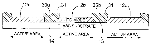
La présente divulgation porte sur une méthode qui permet de fabriquer une diode électroluminescente organique (OLED) où une couche de lissage conforme isolante inerte est déposée sur une structure protubérante. La couche de lissage est configurée pour exposer des parties de la structure sous-jacentes à la couche de lissage et qui définissent des zones actives du dispositif. La couche de lissage inerte est traitée, de préférence par refusion, pour effiler la couche sur les bords échelonnés de la structure, sur les parties exposées. Des couches supplémentaires sont ensuite déposées sur la couche de lissage et sur les parties exposées de la structure. La couche de lissage émousse tous les bords de la couche sous-jacente et fournit des bords obliques advenant un échelon d'une couche à l'autre. Ce procédé résulte en un champ homogène à travers les pixels et la continuité des couches déposées après la couche à résine photosensible.


Abrégé anglais


A method of making an organic light emitting device (OLED) is disclosed
wherein an
inert insulating conformal smoothing layer is deposited over a protruding
structure. The
smoothing layer is patterned to expose portions of the structure underlying
the smoothing
layer and defining active regions of the device. The inert smoothing layer is
treated,
preferably by heat reflow, to taper the layer over the stepped edges of the
structure on the
exposed portions. Additional layers are then deposited over the smoothing
layer and the
exposed portions of the structure. The smoothing layer blunts all underlying
layer edges
and provides sloped edges wherever a step occurs from one layer to another.
This effect
results in a homogeneous field across the pixel and the continuity in the
layers deposited
after the photoresist layer.

Revendications

Note : Les revendications sont présentées dans la langue officielle dans laquelle elles ont été soumises.


I claim:
1. A method of making an organic light emitting device comprising:
forming a structure with stepped edges;
depositing a conformal smoothing layer over said structure, said conformal
smoothing layer having a thickness greater than said structure;
patterning said smoothing layer to expose portions of said structure
underlying
said smoothing layer and defining active regions of said device;
treating said smoothing layer to taper said smoothing layer over said stepped
edges of said structure on said exposed portions; and
depositing additional layers over said smoothing layer and said exposed
portions
of said structure.
2. A method as claimed in claim 1, wherein said smoothing layer is treated by
a heat
reflow treatment.
3. A method as claimed in claim 1 or 2, wherein said smoothing layer is a
layer of
photoresist.
4. A method as claimed in claim 3, wherein said photoresist is spun on to said
structure.
5. A method as claimed in claim 4, wherein said smoothing layer is patterned
by a
lithographic process.
6. A method as claimed in claim 5, wherein said photoresist layer is subjected
to a
bake after patterning to cause said photoresist to reflow.

7. A method as claimed in any one of claims 1 to 6, wherein said structure is
formed
by etching.
8. A method as claimed in claim 7, wherein said structure is an anode.
9. A method as claimed in any one of claims 1 to 8, wherein said additional
layers
are deposited by thermal evaporation.
10. A method as claimed in any one of claims 1 to 9, wherein said additional
layers
comprise a single layer organic light emitting structure and a cathode.
11. A method as claimed in any one of claims 1 to 9, wherein said additional
layers
comprise a multi-layer organic light emitting structure and a cathode
12. A method as claimed in claim 8, wherein said anode is made of indium tin
oxide
(ITO).
13. A method as claimed in claim 8, wherein said anode is deposited on a
transparent
substrate.
14. A method as claimed in claim 13, wherein said transparent substrate is
glass.
15. A method as claimed in any of claims 1 to 14, wherein said smoothing layer
is up
to about 2 µm thick.
16. An organic light emitting device comprising:
a structure with stepped edges;
a patterned conformal smoothing layer extending over said structure and
exposing
portions of said structure underlying said smoothing layer defining active
regions of said
device, said smoothing layer having a thickness greater than said structure
and tapering
over said stepped edges on said exposed portions; and
11

additional layers over said smoothing layer and said exposed portions of said
structure.
17. An organic light emitting device as claimed in claim 16, wherein said
smoothing
layer is a photoresist layer.
18. An organic light emitting device as claimed in claim 16 or 17, wherein
said
structure is an anode.
19. An organic light emitting device of as claimed in any one of claims 16 to
18,
wherein said additional layers comprise a single layer organic light emitting
structure and
a cathode.
20. An organic light emitting device as claimed in claim 16, wherein said
additional
layers comprise a multi-layer organic light emitting structure and a cathode.
21. An organic light emitting device as claimed in claim 18, wherein said
anode is an
indium tin oxide anode deposited on a transparent substrate.
22. An organic light emitting device as claimed in claim 21, wherein said
transparent
substrate is glass.
23. An organic light emitting device as claimed in any one of claims 16 to 22,
wherein
said additional layers include a cathode made of a layer of silver and a layer
of silver
magnesium alloy.
24. An organic light emitting device as claimed in claim 20, wherein said
multi-layer
organic light emitting structure comprises an Alq3 /NPB:Rubrene
(100:1)/NPB/CuPc
stack.
12

Description

Note : Les descriptions sont présentées dans la langue officielle dans laquelle elles ont été soumises.


CA 02397857 2010-12-07
OLED DEVICES WITH PHOTORESIST MASK/SMOOTHING LAYER
FIELD OF THE INVENTION
The invention relates to the field of optical devices, and in particular to
organic light
emitting devices (OLEDs), and to a method of manufacturing such devices.
BACKGROUND OF THE INVENTION
OLEDs have recently shown promise for use as a light source in optical
displays. A
typical structure for an OLED is shown in Figure 1 and consists of a stack of
organic
semiconductor layers 10 between a transparent electrode 12 (usually an indium
tin oxide
(ITO) layer acting as an anode) on a glass substrate 14 and another
electrode16 (usually a
layer of low work function metal, metal alloy or cermet material acting as a
cathode). At
positive bias, electric current will flow through the device and light
emission will occur
between the overlapped area of anode and cathode.
In order to display information, it is necessary to make pixels of the
required shape. This
can be achieved either by patterning the first electrode (anode) or using
shadow masks to
define the shape of the second electrode, or patterning both electrodes
depending on the
application.
The vertical dimension of organic light emitting devices (OLED) is usually
very thin. To
optimize the hole-transport, electron-transport properties and device
efficiency, the total
thickness of the organic layer between the cathode and anode is typically
between 100 nm
and 200 nm. A typical OLED has an electric field of _106V/cm during device
operation.
This high electric field makes OLEDs very sensitive to the edges of patterned
ITO
substrates (the first electrode) or other types of electrode on which the
organic materials is
deposited. Imperfect step coverage of the deposited organic materials will
result in a
substantially higher electric field and higher local current density at that
area. This will
cause the device to break down.
1

CA 02397857 2010-12-07
Figure 2 shows an anode 12 that has been patterned for form three OLED devices
20a,
20b, 20c. The lack of anode material between the devices causes a step between
the
portions of the deposited cathode layer 16a and organic layer l0a located
between the
OLED devices and between the portions of the same layers, 16b, 10b over the
OLED
devices. Figure 2 shows that in some cases the patterned ITO layer 12 or other
type of
electrode layer is thicker than the organic layer 10..Since thermal vacuum
deposition,
which is used to deposit the organic layer 12, is generally non-conformal,
some
uncovered ITO anode area 21 will come into contact with the metal cathode
layer 16
deposited after the deposition of the organic layers 12. This will. cause
massive short
circuits in the devices.
Because of the non-conformal nature of the thermal deposition, when the total
thickness
of ITO anode and organic layers exceeds the thickness of the cathode layer, a
discontinuity 22 may occur in cathode layer where it passes from the OLED to
the area
between the OLEDs. This type of discontinuity will cause device failure in
OLEDs based
on a common cathode (or common anode) design and may also cause device failure
in
individual pixels or segments due to the open circuit between the electrode
layer and
connection pads.
Deposited silicon oxide, aluminum oxide, or silicon nitride is typically used
to define an
emissive area. After the deposition of insulating material, a
photolithographic process and
an etching process are necessary to create pixel areas and sloped edges. Such
a process is
described in U.S. Patent No. 6,069,443. This process is complicated. It
involves dielectric
deposition, a photolithographic process, and at least one etching step for
creating pixel areas.
The deposition of dielectric material is also expensive.
2

CA 02397857 2003-08-13
Various solutions have been proposed in the prior art, all of which are
unsatisfactory for
one reason or another. Mathine et al (U of Arizona) [D.L. Mathine et al, Appl.
Phys.
Lett., 76(26), 2000, p3849], describes the use of PEDOT:PSS (poly(ethylened
ioxythiophene) doped with polystyrenesulfonate) as a buffer layer between a
CMOS
active matrix and the OLED. It is spun-5 on and forms a 20nm thick conformal
layer that
covers the dielectric edges between pixels. It is resistive enough not to
short the different
pixels, and helps charge injection into the hole transport layer. A lift-off
photoresist
pattern is applied prior to PEDOT:PSS so that layer can be lifted off the
connection pads.
The layer is too thin to smooth out underlying structures and is actually part
of the diode.
Shimoda (Seiko, CDT) [Asia Display 98, p2171 use an Si02 "adhesive" layer and
a
polyimide "interval layer" between a TFT active matrix and the PLEDs. Both
have
openings that define the pixels. Shimoda's layer is an insulating and
passivation layer.
The edges are not sloped.
Steward et al (U of Lehigh and Emagin, old FED Corp) [IEDM 98, p871] use two
spin-
on-glass layers for planarization of a TFT matrix. The first layer goes below
the ITO
anode to ensure planarity of the ITO electrode on top of the matrix, and the
second layer
defines pixel openings and smoothes the matrix. The SOG layers are spun, cured
at
300 C, patterned and wet-etched in a certain way so that the organic materials
have good
step coverage.
Jones (Emagin, old FED Corp) [U.S. Patent No 6,069,443] describes the use of a
separator for passive matrix displays with an overhanging profile and an
underlying
insulator that prevents short-circuits from happening when the cathode flows
on top of the
organics edge defined by the overhanging separator. Jones employs an
underlying
3

CA 02397857 2010-12-07
insulator with openings that substantially define pixels, and with tapered
edges to
minimize edge shorts. The purpose of Jones' structure is to prevent short-
circuits.
Smoothing layers have been used in LCDs between the color filters, patterned
first on the
substrate, and the ITO electrode (see for example U.S. Patent No. 5,488,497).
In this case
the goal is to ensure color purity and has nothing to do with field
homogeneity since
liquid crystal layers are very thick compared to the thickness of the
electrodes.
SUMMARY OF THE INVENTION
According to the present invention there is provided a method of making an
organic light
emitting device (OLED) comprising forming a structure with stepped edges;
depositing a
conformal smoothing layer over said structure, said smoothing layer having a
thickness
greater than said structure; patterning said smoothing layer to expose
portions of said
structure underlying said smoothing layer and defining active regions of said
device;
treating said smoothing layer to taper said smoothing layer over said stepped
edges of
said structure on said exposed portions; and depositing additional layers over
said
smoothing layer and said exposed portions of said structure.
In one embodiment the invention provides a photoresist-based smoothing mask
technique
to overcome the difficulties encountered in the prior art in the fabrication
of OLEDs. The
use of a photoresist as a smoothing layer permits direct patterning of the
OLEDs and
simplified sloping by temperature reflow.
In accordance with the principles of the invention the applied smoothing layer
has
openings to define the pixels and blunts all underlying layer edges in order
to ensure that
the thickness of organic layers is as constant as possible everywhere they are
covered by
the top electrode. This arrangement results in a homogeneous field across the
individual
pixels and continuity in the layers. deposited after the photoresist layer.
4

CA 02397857 2003-08-13
A particularly convenient class of material to use for the smoothing layer is
photosensitive resins. Such resins have several advantages. They can be used
in spin
coating and therefore provide a conformal coating smoothing out all edges.
They can be
directly patterned by lithography (exposure and development) without pattern
transfer,
thereby providing a simple process. They reflow during a hard-bake, which in
this case
stabilizes the photoresist and provides a smooth pixel edge. They are of a
similar nature to
the active materials of the OLEDs and therefore will be protected by any
passivation
layers that are applied to ensure the integrity of the OLEDs.
The invention thus relates to a technique which can use commercially available
photoresist as a masking/ smoothing layer to define the emissive and non-
emissive areas
of the light emitting devices. Typical thickness of this layer is in the up to
about 2
microns, for example, 1 - 2 microns, that is thick enough to cover all the
steps produced
after ITO etching. During the baking process, the photoresist reflows,
providing a tapered
slope at the edge. This photoresist layer therefore not only functions as a
mask layer to
define an active area but also blunts the steep edges produced by ITO
patterning and
provides tapered edges to maintain continuity in the cathode layer so that the
device can
be connected to the outside world. Subsequently, organic layers and a metal
cathode are
applied to complete the process. In this way, short circuits and
discontinuities in cathode
can be substantially avoided.
The invention also provides an organic light emitting device comprising a
structure with
stepped edges; a patterned conformal smoothing layer extending over said
structure and
exposing portions of said structure underlying said smoothing layer defining
active
regions of said device, said smoothing layer having a thickness greater than
said structure
and tapering over said stepped edges of said structure on said exposed
portions; and
5

CA 02397857 2010-12-07
additional organic and metal layers over said smoothing layer and said exposed
portions
of said structure.
BRIEF DESCRIPTION OF THE DRAWINGS
The invention will now be described in more detail, by way of example only,
with
reference to the accompanying drawings, in which:
Figure 1 is a schematic illustration of a typical OLED;
Figure 2 is a schematic illustration of a plurality of OLEDs and possible
defects
encountered in such devices;
Figures 3 and 4 illustrate process steps in accordance with one embodiment of
the
invention;
Figure 5 shows a plurality of OLEDs on a wafer made according to one
embodiment of
the invention; and
Figure 6 is a set of graphs showing the characteristics of OLEDs made
according to one
embodiment of the invention.
DETAILED DESCRIPTION OF THE INVENTION
A method of making an OLED in accordance with one embodiment of the invention
will
now be described with reference Figures 3 and 4: An ITO coated glass substrate
14 is
cleaned in a conventional manner. The ITO layer 12 is then patterned and
etched to
produce individual anodes 12a, 12b, 12c. It will be appreciated that other
suitable
transparent materials can be employed for the substrate.
A layer of commercial photoresist 30 approximately up to approximately 2 tm
thick is
applied between the individual anodes. This layer is exposed and developed to
leave the
individual columns 30a, 30b of photoresist protruding between the individual
anodes and
overhanging slightly over the step edges 31 of the anodes 12.
6

CA 02397857 2003-08-13
The wafer is then subjected to a baking step in which the photoresist reflows
to produce
columns with tapered edges 32 overhanging the exposed portions of the
individual anodes
as shown in Figure 4.
The photoresist layer acts as a mask for the subsequent deposition by thermal
evaporation
of the organic layer 10 and the metal cathode layer 16. As will be seen in
Figure 5, these
two layers 10, 16 smoothly follow the contour of the photoresist layer 30 and
as result
steps, which might cause short-circuits, and sharp discontinuities are
avoided. No short
circuits are formed in the regions 23, 24, and no discontinuity is present in
region 25.
Figure 6 shows the characteristics of OLEDs made using the above process. The
devices
were made of a multi-layer organic stack on an ITO (120 rim) anode. The
organic stack
consisted of CuPc(5nm)NPB(30nm)/NPB:Rubrene(100:1, 40 nm) /A1g3(40nm). The
chemical structure of the compounds is as follows:
,I A1q3
KN.
3
NPB
7

CA 02397857 2003-08-13
Rubrene
N
N
CuPc
The metal cathode 16 consisted of a layer of Ag(60nm) and a layer of an Mg:Ag
alloy
(10:1, 100nm).
As can be seen in the graphs shown in Figure 6, these devices show very good
characteristics with respect to current-voltage and luminance properties
compared to
devices made without the smoothing layer. The photoresist smoothing layer
blunts all
underlying layer edges and provides sloped edge wherever a step occurs from
one layer to
another. This process ensures the thickness of the organic layers as constant
as possible
everywhere they are covered by the top electrode, thus the use of a smoothing
layer
results in a homogeneous field across the pixel.
The use of a photoresist as mask/smoothing layer has proved to ensure the
field
homogeneity and good step-coverage in OLEDs. The photoresist layer behaves
like a
good insulating layer.
8

CA 02397857 2003-08-13
This described method uses a simple lithographic process, avoiding complicated
PECVD
(plasma enhanced chemical vapor deposition) or other deposition process for
insulating
layer, avoiding an etching process for producing sloped edges. One simple
photolithographic step produces insulting layer, pixel areas and tapered
edges.
The organic light emitting devices in accordance with the invention have
emissive areas
and non-emissive areas, the emissive areas defining a plurality of pixels. The
photoresist
layer covers the non-emissive areas. The thickness of the layer is larger than
the thickness
of the electrode of each pixel onto which the photoresist is applied
The invention is further directed to an organic light emitting device having
emissive areas
and non-emissive areas, the emissive areas defining a plurality of pixels. The
device
comprises a patterned first electrode defining the emissive areas, a
photoresist layer
covering non-emissive areas, the thickness of the layer being larger than the
first
electrode and edges of the photoresist layer being tapered by reflow. The
device further
comprises one or more organic layers deposited on the first electrode and the
photoresist
layer, and a second electrode on the organic layer.
The OLED can be formed into multipixel displays and the like using
conventional
technology. The method has been tested in more than three hundred batches, and
proved
to be reliable and reproducible.
9

Dessin représentatif
Une figure unique qui représente un dessin illustrant l'invention.
États administratifs

2024-08-01 : Dans le cadre de la transition vers les Brevets de nouvelle génération (BNG), la base de données sur les brevets canadiens (BDBC) contient désormais un Historique d'événement plus détaillé, qui reproduit le Journal des événements de notre nouvelle solution interne.

Veuillez noter que les événements débutant par « Inactive : » se réfèrent à des événements qui ne sont plus utilisés dans notre nouvelle solution interne.

Pour une meilleure compréhension de l'état de la demande ou brevet qui figure sur cette page, la rubrique Mise en garde , et les descriptions de Brevet , Historique d'événement , Taxes périodiques et Historique des paiements devraient être consultées.

Historique d'événement

Description Date
Inactive : CIB en 1re position 2024-01-08
Inactive : CIB attribuée 2024-01-08
Inactive : CIB expirée 2023-01-01
Inactive : CIB enlevée 2022-12-31
Le délai pour l'annulation est expiré 2015-08-13
Lettre envoyée 2014-08-13
Requête visant le maintien en état reçue 2013-08-07
Inactive : TME en retard traitée 2012-08-21
Lettre envoyée 2012-08-13
Accordé par délivrance 2012-05-29
Inactive : Page couverture publiée 2012-05-28
Préoctroi 2012-03-20
Inactive : Taxe finale reçue 2012-03-20
Un avis d'acceptation est envoyé 2011-09-26
Lettre envoyée 2011-09-26
Un avis d'acceptation est envoyé 2011-09-26
Inactive : Approuvée aux fins d'acceptation (AFA) 2011-09-22
Inactive : CIB désactivée 2011-07-29
Modification reçue - modification volontaire 2010-12-07
Inactive : Dem. de l'examinateur par.30(2) Règles 2010-06-07
Inactive : CIB enlevée 2010-01-28
Inactive : CIB attribuée 2010-01-28
Inactive : CIB en 1re position 2010-01-28
Inactive : CIB expirée 2010-01-01
Lettre envoyée 2006-12-07
Exigences pour une requête d'examen - jugée conforme 2006-11-17
Toutes les exigences pour l'examen - jugée conforme 2006-11-17
Requête d'examen reçue 2006-11-17
Inactive : CIB de MCD 2006-03-12
Demande visant la révocation de la nomination d'un agent 2004-10-21
Demande visant la nomination d'un agent 2004-10-21
Lettre envoyée 2004-08-04
Inactive : Lettre officielle 2004-08-04
Lettre envoyée 2004-08-04
Lettre envoyée 2004-07-22
Demande publiée (accessible au public) 2004-02-13
Inactive : Page couverture publiée 2004-02-12
Exigences relatives à la nomination d'un agent - jugée conforme 2003-09-22
Inactive : Lettre officielle 2003-09-22
Exigences relatives à la révocation de la nomination d'un agent - jugée conforme 2003-09-22
Modification reçue - modification volontaire 2003-08-13
Demande visant la révocation de la nomination d'un agent 2003-08-12
Demande visant la nomination d'un agent 2003-08-12
Inactive : CIB attribuée 2002-11-20
Inactive : CIB en 1re position 2002-11-20
Inactive : Certificat de dépôt - Sans RE (Anglais) 2002-09-24
Lettre envoyée 2002-09-24
Demande reçue - nationale ordinaire 2002-09-23

Historique d'abandonnement

Il n'y a pas d'historique d'abandonnement

Taxes périodiques

Le dernier paiement a été reçu le 2011-06-10

Avis : Si le paiement en totalité n'a pas été reçu au plus tard à la date indiquée, une taxe supplémentaire peut être imposée, soit une des taxes suivantes :

  • taxe de rétablissement ;
  • taxe pour paiement en souffrance ; ou
  • taxe additionnelle pour le renversement d'une péremption réputée.

Les taxes sur les brevets sont ajustées au 1er janvier de chaque année. Les montants ci-dessus sont les montants actuels s'ils sont reçus au plus tard le 31 décembre de l'année en cours.
Veuillez vous référer à la page web des taxes sur les brevets de l'OPIC pour voir tous les montants actuels des taxes.

Historique des taxes

Type de taxes Anniversaire Échéance Date payée
Taxe pour le dépôt - générale 2002-08-13
TM (demande, 2e anniv.) - générale 02 2004-08-13 2004-08-09
TM (demande, 3e anniv.) - générale 03 2005-08-15 2005-07-07
TM (demande, 4e anniv.) - générale 04 2006-08-14 2006-08-04
Requête d'examen - générale 2006-11-17
TM (demande, 5e anniv.) - générale 05 2007-08-13 2007-07-12
TM (demande, 6e anniv.) - générale 06 2008-08-13 2008-08-08
TM (demande, 7e anniv.) - générale 07 2009-08-13 2009-06-23
TM (demande, 8e anniv.) - générale 08 2010-08-13 2010-07-07
TM (demande, 9e anniv.) - générale 09 2011-08-15 2011-06-10
Taxe finale - générale 2012-03-20
Annulation de la péremption réputée 2012-08-13 2012-08-21
TM (brevet, 10e anniv.) - générale 2012-08-13 2012-08-21
TM (brevet, 11e anniv.) - générale 2013-08-13 2013-08-07
Titulaires au dossier

Les titulaires actuels et antérieures au dossier sont affichés en ordre alphabétique.

Titulaires actuels au dossier
NATIONAL RESEARCH COUNCIL OF CANADA
Titulaires antérieures au dossier
YE TAO
Les propriétaires antérieurs qui ne figurent pas dans la liste des « Propriétaires au dossier » apparaîtront dans d'autres documents au dossier.
Documents

Pour visionner les fichiers sélectionnés, entrer le code reCAPTCHA :


Pour visualiser une image, cliquer sur un lien dans la colonne description du document. Pour télécharger l'image (les images), cliquer l'une ou plusieurs cases à cocher dans la première colonne et ensuite cliquer sur le bouton "Télécharger sélection en format PDF (archive Zip)" ou le bouton "Télécharger sélection (en un fichier PDF fusionné)".

Liste des documents de brevet publiés et non publiés sur la BDBC .

Si vous avez des difficultés à accéder au contenu, veuillez communiquer avec le Centre de services à la clientèle au 1-866-997-1936, ou envoyer un courriel au Centre de service à la clientèle de l'OPIC.


Description du
Document 
Date
(aaaa-mm-jj) 
Nombre de pages   Taille de l'image (Ko) 
Dessin représentatif 2003-01-12 1 11
Description 2002-08-12 6 243
Abrégé 2002-08-12 1 32
Revendications 2002-08-12 1 27
Description 2003-08-12 9 347
Abrégé 2003-08-12 1 21
Revendications 2003-08-12 3 93
Description 2010-12-06 9 356
Revendications 2010-12-06 3 93
Dessins 2010-12-06 6 83
Dessin représentatif 2011-09-22 1 8
Courtoisie - Certificat d'enregistrement (document(s) connexe(s)) 2002-09-23 1 112
Certificat de dépôt (anglais) 2002-09-23 1 162
Rappel de taxe de maintien due 2004-04-13 1 110
Accusé de réception de la requête d'examen 2006-12-06 1 178
Avis du commissaire - Demande jugée acceptable 2011-09-25 1 163
Avis concernant la taxe de maintien 2012-08-20 1 170
Quittance d'un paiement en retard 2012-08-20 1 163
Avis concernant la taxe de maintien 2014-09-23 1 171
Correspondance 2003-08-11 2 63
Correspondance 2003-09-21 1 17
Correspondance 2003-09-21 1 19
Correspondance 2004-07-21 2 14
Correspondance 2004-08-03 1 22
Correspondance 2004-08-03 1 15
Taxes 2004-06-28 1 38
Correspondance 2004-10-20 2 65
Correspondance 2012-03-19 1 30
Taxes 2013-08-06 1 32
Correspondance de la poursuite 2003-08-12 17 569