Note: Descriptions are shown in the official language in which they were submitted.
CA 02415700 2003-O1-07
WO 02/04999 PCT/USO1/20433
1
GRADED INDEX WAVEGUIDE
PRIORITY INFORMATION
This application claims priority from provisional application Ser. No.
60/217,167 filed July 10, 2000.
BACKGROUND OF THE INVENTION
The invention is in the field of optics, and specifically relates to optical
waveguides.
Roughness scattering is one of the major sources of transmission loss in
dielectric
optical waveguides. The roughness at the core/cladding interface, where an
abrupt
change in the refractive index occurs, is responsible for such a scattering.
It is
particularly severe for high index difference (difference in the refractive
indices
between the core and the cladding) waveguides, since the scattering loss
scales with
index difference. The relationship between the scattering loss and the index
difference
can be found in Journal of Lightwave Technology 12, 790-796 (1994) by Suzuki
et. al.
A high index difference waveguide typically has an index difference equal to
or
larger than 0.3 in a square channel waveguide configuration. A channel
waveguide is a
dielectric waveguide whose core is surrounded by a cladding that is composed
of a
2 0 material or materials with refractive indices lower than that of the core,
and wherein
the peak optical intensity resides in the core. High index difference
waveguides can be
defined in other waveguide geometries. In waveguide configurations that are
difference from a channel waveguide, a high index difference waveguide is
defined as
one that has a mode-field size similar to that of a high index difference
channel
2 5 waveguide (within 50 % difference in cross-sectional area). In these
waveguides, a
cladding is defined as a region where the evanescent field of optical modes
exists.
Graded index waveguides are conventionally used in fiber optics to minimize
modal dispersion. U.S. Pat. No. 4,412,722, issued to Carnevale et al. shows
optical fiber
waveguide with its index of refraction graded in the radial direction so as to
yield low
3 0 total dispersion. The index gradient is achieved by a diffusion process.
Grading the index at the core/cladding interfaces in planar waveguides is also
shown
in the prior art. Many publications including Applied Optics, Vol. 25, No. 9,
May 1956 by
Danko et. al. and Proceedings of SPIE, Vol. 2943 by Augusciuk et. al., show
the fabrication
CA 02415700 2003-O1-07
WO 02/04999 PCT/USO1/20433
2
of graded index channel waveguides by an ion-exchange process. In an ion-
exchange
process, the index of the waveguide core is raised above the waveguide
cladding by
inserting ions into the targeted region and annealing the waveguide to form a
new chemical
compound with a high refractive index than the previous material.
Proceedings of SPIE, Vol. 1774 by Shih et. al. shows a graded index waveguide
that is formed by photolithography. A photo-sensitive polymer is used as the
waveguide
material that changes the index according to the intensity of the light that
impinges on it.
In the prior art, waveguides are formed by methods of increasing the index of
the
targeted region, which becomes the waveguide core, over the rest. As a result
of these
methods, the index is graded from the core to the cladding.
SiJNiMARY OF THE INVENTION
The graded index waveguide of the invention reduces the effect of the
core/cladding interface roughness on the scattering loss, therefore reducing
the loss. By
gradually changing the index at the core/cladding interface, the scattering
loss is
minimized, since the index jump from the core to the cladding is moderated by
the
presence of the graded index layer at the interface. The gradual index change
at the
interface results in the lower scattering loss since the mode traveling in the
waveguide
experiences less index difference at the core/cladding interfaces.
2 o In accordance with one embodiment, the invention is a planar waveguide
that has
a graded index layer between the core and the cladding of a dielectric
waveguide, created
by either deposition, growth, or a chemical reaction, before the final
cladding is put
down. The graded index layer is created after the waveguide core is already
formed.
This is different from the prior arts where the graded index profile is
automatically
2 5 created when the waveguide core is being formed. In this invention, a
graded index
profile exists at the core/cladding interface, reducing the scattering losses
due to interface
roughness.
It is an object of the invention to minimize scattering loss by altering the
abrupt
index jump from that of the core to that of the cladding of a planar
waveguide, by grading
3 0 the index at the interface. Many index profiles at the waveguide
core/cladding are possible
for reduction of the waveguide loss. It is another object of the invention to
show that such a
graded index interface between the core and the cladding can be achieved by
methods of
adding materials such as thin film growth or deposition on the waveguide core.
Such a
graded index interface between the core and the cladding can be achieved by
methods of
CA 02415700 2003-O1-07
WO 02/04999 PCT/USO1/20433
3
altering materials such as a chemical reaction on the surface of the waveguide
core. It is
yet another object of the invention to minimize modal and polarization
dispersion of a planar
waveguide using the graded index design.
BRIEF DESCRIPTION OF THE DRAWINGS
Figure 1 is a cross-section view of an exemplary embodiment of a graded index
planar waveguide in accordance with the invention;
Figure 2 is a graph of the index profile along the index cross-section shown
in
Figure l; and
Figure 3 is a diagram of the processing steps for fabricating a graded index
waveguide using a thin film deposition technique in a accordance with the
invention.
DETAILED DESCRIPTION OF THE INVENTION
Figure 1 is a cross-section view of an exemplary embodiment of a graded index
planar waveguide 100 in accordance with the invention. The waveguide includes
a
substrate for mechanical support, a first low index cladding 104, a high index
core 101, a
graded index layer 103 and a second low index cladding 102. The refractive
index of the
core 101, n1, is larger than that of the claddings 102 and 104, n~ and n4. A
unique feature
of this waveguide is the presence of the graded index layer 103 between the
core 101 and
2 0 the cladding 102, whose index gradually varies from that of the high index
core to that of
the low index cladding. Scattering of light due to the rough interfaces
between the core
and the cladding is minimized since the index change from core to cladding is
gradual.
The index cross-section of the core, cladding, and the graded index layer in
Figure 1
is demonstrated in the graph of Figure 2. The index profile of the graded
index layer need
2 5 not be linear, as shown in Figure 2. The index in the core 101 is higher
than that in the
cladding 102. The index in the graded index layer is graded so that there is a
less abrupt
jump in index between the core and cladding. The index of the graded index
layer can be
changed between low and high index regions using any index profiles such as
curves and
staircase steps. Any profile that reduces the index jump from core to cladding
at the
3 0 interface will lower the scattering loss. The graded index layer should be
designed so that
the loss is optimally minimized. At the same time, the design should address
the change in
the confinement factor (how tightly light is confined in the waveguide core)
due to the
presence of the graded index layer, which will play a role in waveguide
devices such as
CA 02415700 2003-O1-07
WO 02/04999 PCT/USO1/20433
4
bends. A proper design of the graded index layer can also reduce modal and
polarization
dispersion.
An additional graded index layer can be inserted between the core 101 and the
cladding 104 if the interface between them is rough. This layer will also make
the
waveguide look more symmetric, reducing polarization dispersion.
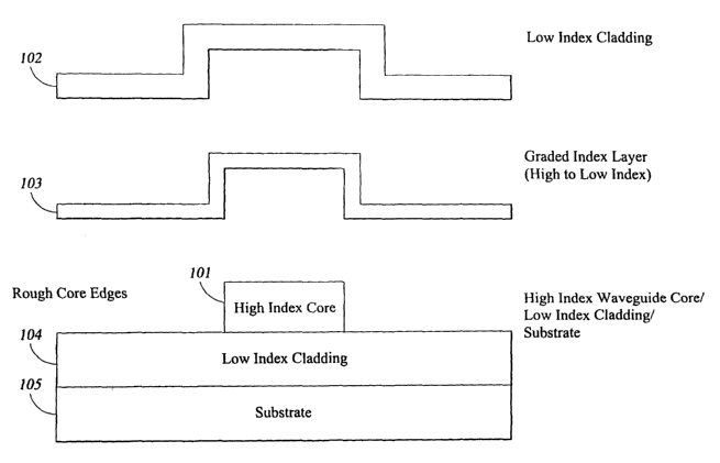
Figure 3 is a diagram of an exemplary fabrication process of a graded index
waveguide in accordance with the invention. The patterned waveguide core 101
has
rough edges arising from the patterning techniques used. Thereafter, the
graded index
layer 103 is deposited. During the deposition process, the index of the layer
is varied
1 o from that of core to that of cladding. The index grading can be achieved
by varying the
chemical composition of the layer. Finally, the cladding layer 102 is
deposited on top.
Such a gradient in the index can also be obtained by a thin film growth
method.
During the growth process, the composition of the impinging material at the
waveguide
core surface can be changed to obtain an index gradient.
Another method of making graded index waveguide is to obtain a gradient in the
atomic composition at the surface of the waveguide core from a chemical
reaction. The
composition of the waveguide core can be altered by chemical reactions that
yield
products that are transparent to the wavelength of interest, and has an index
lower than
that of the core. Since the concentration of the reactant of the chemical
reactions is
2 0 highest at the surface and decreases exponentially due to the diffusion of
the reactant into
the core material, there will be a concentration gradient of the product into
the core
material starting from the surface. The index near the surface will be graded
according
to the chemical composition gradient.
A graded index silicon nitride waveguide is an example of this type of
2 5 waveguides. As shown in Figure 1, the graded index layer in this case is a
silicon
oxynitride layer whose index varies from that of a silicon nitride core to
that of a silicon
dioxide cladding. The index change is achieved by changing the ratio of oxygen
and
nitrogen in silicon oxynitride layer. Deposition techniques such as chemical
vapor
deposition or sputtering can be used for depositing this layer.
3 0 A graded index germanium(Ge)/silicon(Si) waveguide is an example of a
graded
index waveguide obtained by a thin film growth technique. When germanium is
the core
material and silicon is the cladding material, SiXGeI_X can be the graded
index layer,
whose index is graded during the growth process.
CA 02415700 2003-O1-07
WO 02/04999 PCT/USO1/20433
An example of obtaining a graded index layer using a chemical reaction can be
illustrated with a waveguide whose core is silicon nitride and the cladding
silicon dioxide.
By subjecting patterned a silicon nitride waveguide core to oxidizing agents,
a silicon
oxynitride layer is formed at the surface. Since this process is controlled by
diffusion of the
5 oxidizing agents into the silicon nitride waveguide core, the concentration
gradient of
oxygen and nitrogen is created at the surface, with the surface having the
highest level of
oxygen. The concentration of oxygen decreases into the waveguide core while
that of
nitrogen increases.
Although the present invention has been shown and described with respect to
'1 o several preferred embodiments thereof, various changes, omissions and
additions to the
form and detail thereof, may be made therein, without departing from the
spirit and
scope of the invention.
What is claimed is: