Sélection de la langue

Search

Sommaire du brevet 2415700 

Énoncé de désistement de responsabilité concernant l'information provenant de tiers

Une partie des informations de ce site Web a été fournie par des sources externes. Le gouvernement du Canada n'assume aucune responsabilité concernant la précision, l'actualité ou la fiabilité des informations fournies par les sources externes. Les utilisateurs qui désirent employer cette information devraient consulter directement la source des informations. Le contenu fourni par les sources externes n'est pas assujetti aux exigences sur les langues officielles, la protection des renseignements personnels et l'accessibilité.

Disponibilité de l'Abrégé et des Revendications

L'apparition de différences dans le texte et l'image des Revendications et de l'Abrégé dépend du moment auquel le document est publié. Les textes des Revendications et de l'Abrégé sont affichés :

  • lorsque la demande peut être examinée par le public;
  • lorsque le brevet est émis (délivrance).
(12) Demande de brevet: (11) CA 2415700
(54) Titre français: GUIDE D'ONDE A GRADIENT D'INDICE
(54) Titre anglais: GRADED INDEX WAVEGUIDE
Statut: Réputée abandonnée et au-delà du délai pour le rétablissement - en attente de la réponse à l’avis de communication rejetée
Données bibliographiques
(51) Classification internationale des brevets (CIB):
  • G02B 06/00 (2006.01)
  • G02B 06/10 (2006.01)
  • G02B 06/12 (2006.01)
  • G02B 06/122 (2006.01)
  • G02B 06/13 (2006.01)
  • G02B 06/132 (2006.01)
(72) Inventeurs :
  • LEE, KEVIN K. (Etats-Unis d'Amérique)
  • LIM, DESMOND (Etats-Unis d'Amérique)
  • WADA, KAZUMI (Etats-Unis d'Amérique)
  • KIMERLING, LIONEL C. (Etats-Unis d'Amérique)
(73) Titulaires :
  • MASSACHUSETTS INSTITUTE OF TECHNOLOGY
(71) Demandeurs :
  • MASSACHUSETTS INSTITUTE OF TECHNOLOGY (Etats-Unis d'Amérique)
(74) Agent: SMART & BIGGAR LP
(74) Co-agent:
(45) Délivré:
(86) Date de dépôt PCT: 2001-06-27
(87) Mise à la disponibilité du public: 2002-01-17
Requête d'examen: 2003-01-07
Licence disponible: S.O.
Cédé au domaine public: S.O.
(25) Langue des documents déposés: Anglais

Traité de coopération en matière de brevets (PCT): Oui
(86) Numéro de la demande PCT: PCT/US2001/020433
(87) Numéro de publication internationale PCT: US2001020433
(85) Entrée nationale: 2003-01-07

(30) Données de priorité de la demande:
Numéro de la demande Pays / territoire Date
60/217,167 (Etats-Unis d'Amérique) 2000-07-10

Abrégés

Abrégé français

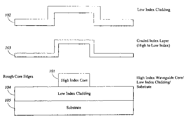
Cette invention concerne un guide d'onde planaire comportant une couche à gradient d'indice à l'interface noyau/gaine dans le but de réduire les pertes par diffusion dues à la rugosité de cette interface. Au niveau de l'interface noyau/gaine, l'indice de réfraction passe progressivement de celui du noyau à celui de la gaine par suite de la présence d'une couche à gradient d'indice. Cette couche à gradient d'indice réduit la diffusion de la lumière dans le guide d'onde en atténuant l'effet de la rugosité au niveau de l'interface abrupte entre le noyau et la gaine. Correctement conçue, la couche à gradient d'indice permet également de diminuer la dispersion modale et de polarisation du mode optique qui se déplace dans le guide d'onde.


Abrégé anglais


A planar waveguide that has a graded index layer at the core/cladding
interface to reduce scattering losses due to core/classing interfave
roughness. The refractive index at the core/cladding interface is changed from
that of the core to that of cladding gradually by having a graded index layer.
The graded index layer reduces the scattering of light traveling in the
waveguide by reducing the effect of the roughness at the abrupt interface
between the core and the cladding. Using a proper design, the graded index
layer also minimizes the modal and polarization dispersion of the optical mode
traveling in the waveguide.

Revendications

Note : Les revendications sont présentées dans la langue officielle dans laquelle elles ont été soumises.


CLAIMS
6
1. A dielectric waveguide comprising:
a first cladding layer on a substrate;
a core provided on said first cladding layer;
a graded index layer provided on said core; and
a second cladding layer provided on said graded index layer.
2. The waveguide of claim 1, wherein said graded index layer is created
separately from said core.
3. The waveguide of claim 1, wherein said core comprises a patterned layer.
4. The waveguide of claim 1, wherein said graded index layer reduces
scattering loss.
5. The waveguide of claim 1, wherein said graded index layer reduces
polarization or modal dispersion.
6. The waveguide of claim 1, wherein the refractive index of said graded index
layer changes from that of said core to that of said second cladding layer in
cross-section.
7. The waveguide of claim 1, wherein said graded index layer has a linear or a
non-linear index profile in cross-section.
8. The waveguide of claim 1, wherein said graded index layer has a continuous
or a segmented index profile in cross-section.
9. The waveguide of claim 1, wherein said graded index layer is created by
methods of adding materials
10. The waveguide of claim 9, wherein said graded index layer is created by
thin
film growth or deposition.
11. The waveguide of claim 1, wherein said graded index layer is created by
methods of altering the chemical composition of materials.
12. The waveguide of claim 11, wherein said graded index layer is created by
chemical reaction.

13. The waveguide of claim 1, wherein said first and second cladding layers
comprise regions of materials that have lower refractive index than that of
said core.
14. A waveguide of claim 1, wherein said core and said graded index layer
comprise silicon and nitrogen in chemical composition.
15. The waveguide of claim 1, wherein said core and said graded index layer
comprise germanium in chemical composition.
16. A planar dielectric waveguide, comprising:
a first cladding layer on a substrate;
a core provided on said first cladding layer;
a graded index layer provided on said core; and
a second cladding layer provided on said graded index layer, wherein
said core and said cladding layers form a high index difference waveguide
whose mode-field size is similar within 50 % difference in area as a channel
waveguide
whose index difference is equal to or above 0.3.
17. The waveguide of claim 16, wherein said graded index layer is created
separately from said core.
18. The waveguide of claim 16, wherein said core comprises a patterned layer.
19. The waveguide of claim 16, wherein said graded index layer reduces
scattering loss.
20. The waveguide of claim 16, wherein said graded index layer reduces
polarization or modal dispersion.
21. The waveguide of claim 16, wherein the refractive index of said graded
index layer changes from that of said core to that of said second cladding
layer in cross-
section.
22. The waveguide of claim 16, wherein said graded index layer has a linear or
a
non-linear index profile in cross-section.

8
23. The waveguide of claim 16, wherein said graded index layer has a
continuous or a segmented index profile in cross-section.
24. The waveguide of claim 16, wherein said graded index layer is created by
methods of adding materials.
25. The waveguide of claim 24, wherein said graded index layer is created by
thin film growth or deposition.
26. The waveguide of claim 16, wherein said graded index layer is created by
methods of altering the chemical composition of materials.
27. The waveguide of claim 26, wherein said graded index layer is created by
chemical reaction.
28. The waveguide of claim 16, wherein said cladding layers comprise regions
of
materials that have lower refractive index than that of said core.
29. The waveguide of claim 16, wherein said core and said graded index layer
comprise silicon and nitrogen in chemical composition.
30. The waveguide of claim 16, wherein said core and said graded index layer
comprise germanium in chemical composition.
31. A method of fabricating a dielectric waveguide comprising:
providing a first cladding layer on a substrate;
providing a waveguide core on said first cladding layer;
providing a graded index layer on said core; and
providing a second cladding layer on said graded index layer.

Description

Note : Les descriptions sont présentées dans la langue officielle dans laquelle elles ont été soumises.


CA 02415700 2003-O1-07
WO 02/04999 PCT/USO1/20433
1
GRADED INDEX WAVEGUIDE
PRIORITY INFORMATION
This application claims priority from provisional application Ser. No.
60/217,167 filed July 10, 2000.
BACKGROUND OF THE INVENTION
The invention is in the field of optics, and specifically relates to optical
waveguides.
Roughness scattering is one of the major sources of transmission loss in
dielectric
optical waveguides. The roughness at the core/cladding interface, where an
abrupt
change in the refractive index occurs, is responsible for such a scattering.
It is
particularly severe for high index difference (difference in the refractive
indices
between the core and the cladding) waveguides, since the scattering loss
scales with
index difference. The relationship between the scattering loss and the index
difference
can be found in Journal of Lightwave Technology 12, 790-796 (1994) by Suzuki
et. al.
A high index difference waveguide typically has an index difference equal to
or
larger than 0.3 in a square channel waveguide configuration. A channel
waveguide is a
dielectric waveguide whose core is surrounded by a cladding that is composed
of a
2 0 material or materials with refractive indices lower than that of the core,
and wherein
the peak optical intensity resides in the core. High index difference
waveguides can be
defined in other waveguide geometries. In waveguide configurations that are
difference from a channel waveguide, a high index difference waveguide is
defined as
one that has a mode-field size similar to that of a high index difference
channel
2 5 waveguide (within 50 % difference in cross-sectional area). In these
waveguides, a
cladding is defined as a region where the evanescent field of optical modes
exists.
Graded index waveguides are conventionally used in fiber optics to minimize
modal dispersion. U.S. Pat. No. 4,412,722, issued to Carnevale et al. shows
optical fiber
waveguide with its index of refraction graded in the radial direction so as to
yield low
3 0 total dispersion. The index gradient is achieved by a diffusion process.
Grading the index at the core/cladding interfaces in planar waveguides is also
shown
in the prior art. Many publications including Applied Optics, Vol. 25, No. 9,
May 1956 by
Danko et. al. and Proceedings of SPIE, Vol. 2943 by Augusciuk et. al., show
the fabrication

CA 02415700 2003-O1-07
WO 02/04999 PCT/USO1/20433
2
of graded index channel waveguides by an ion-exchange process. In an ion-
exchange
process, the index of the waveguide core is raised above the waveguide
cladding by
inserting ions into the targeted region and annealing the waveguide to form a
new chemical
compound with a high refractive index than the previous material.
Proceedings of SPIE, Vol. 1774 by Shih et. al. shows a graded index waveguide
that is formed by photolithography. A photo-sensitive polymer is used as the
waveguide
material that changes the index according to the intensity of the light that
impinges on it.
In the prior art, waveguides are formed by methods of increasing the index of
the
targeted region, which becomes the waveguide core, over the rest. As a result
of these
methods, the index is graded from the core to the cladding.
SiJNiMARY OF THE INVENTION
The graded index waveguide of the invention reduces the effect of the
core/cladding interface roughness on the scattering loss, therefore reducing
the loss. By
gradually changing the index at the core/cladding interface, the scattering
loss is
minimized, since the index jump from the core to the cladding is moderated by
the
presence of the graded index layer at the interface. The gradual index change
at the
interface results in the lower scattering loss since the mode traveling in the
waveguide
experiences less index difference at the core/cladding interfaces.
2 o In accordance with one embodiment, the invention is a planar waveguide
that has
a graded index layer between the core and the cladding of a dielectric
waveguide, created
by either deposition, growth, or a chemical reaction, before the final
cladding is put
down. The graded index layer is created after the waveguide core is already
formed.
This is different from the prior arts where the graded index profile is
automatically
2 5 created when the waveguide core is being formed. In this invention, a
graded index
profile exists at the core/cladding interface, reducing the scattering losses
due to interface
roughness.
It is an object of the invention to minimize scattering loss by altering the
abrupt
index jump from that of the core to that of the cladding of a planar
waveguide, by grading
3 0 the index at the interface. Many index profiles at the waveguide
core/cladding are possible
for reduction of the waveguide loss. It is another object of the invention to
show that such a
graded index interface between the core and the cladding can be achieved by
methods of
adding materials such as thin film growth or deposition on the waveguide core.
Such a
graded index interface between the core and the cladding can be achieved by
methods of

CA 02415700 2003-O1-07
WO 02/04999 PCT/USO1/20433
3
altering materials such as a chemical reaction on the surface of the waveguide
core. It is
yet another object of the invention to minimize modal and polarization
dispersion of a planar
waveguide using the graded index design.
BRIEF DESCRIPTION OF THE DRAWINGS
Figure 1 is a cross-section view of an exemplary embodiment of a graded index
planar waveguide in accordance with the invention;
Figure 2 is a graph of the index profile along the index cross-section shown
in
Figure l; and
Figure 3 is a diagram of the processing steps for fabricating a graded index
waveguide using a thin film deposition technique in a accordance with the
invention.
DETAILED DESCRIPTION OF THE INVENTION
Figure 1 is a cross-section view of an exemplary embodiment of a graded index
planar waveguide 100 in accordance with the invention. The waveguide includes
a
substrate for mechanical support, a first low index cladding 104, a high index
core 101, a
graded index layer 103 and a second low index cladding 102. The refractive
index of the
core 101, n1, is larger than that of the claddings 102 and 104, n~ and n4. A
unique feature
of this waveguide is the presence of the graded index layer 103 between the
core 101 and
2 0 the cladding 102, whose index gradually varies from that of the high index
core to that of
the low index cladding. Scattering of light due to the rough interfaces
between the core
and the cladding is minimized since the index change from core to cladding is
gradual.
The index cross-section of the core, cladding, and the graded index layer in
Figure 1
is demonstrated in the graph of Figure 2. The index profile of the graded
index layer need
2 5 not be linear, as shown in Figure 2. The index in the core 101 is higher
than that in the
cladding 102. The index in the graded index layer is graded so that there is a
less abrupt
jump in index between the core and cladding. The index of the graded index
layer can be
changed between low and high index regions using any index profiles such as
curves and
staircase steps. Any profile that reduces the index jump from core to cladding
at the
3 0 interface will lower the scattering loss. The graded index layer should be
designed so that
the loss is optimally minimized. At the same time, the design should address
the change in
the confinement factor (how tightly light is confined in the waveguide core)
due to the
presence of the graded index layer, which will play a role in waveguide
devices such as

CA 02415700 2003-O1-07
WO 02/04999 PCT/USO1/20433
4
bends. A proper design of the graded index layer can also reduce modal and
polarization
dispersion.
An additional graded index layer can be inserted between the core 101 and the
cladding 104 if the interface between them is rough. This layer will also make
the
waveguide look more symmetric, reducing polarization dispersion.
Figure 3 is a diagram of an exemplary fabrication process of a graded index
waveguide in accordance with the invention. The patterned waveguide core 101
has
rough edges arising from the patterning techniques used. Thereafter, the
graded index
layer 103 is deposited. During the deposition process, the index of the layer
is varied
1 o from that of core to that of cladding. The index grading can be achieved
by varying the
chemical composition of the layer. Finally, the cladding layer 102 is
deposited on top.
Such a gradient in the index can also be obtained by a thin film growth
method.
During the growth process, the composition of the impinging material at the
waveguide
core surface can be changed to obtain an index gradient.
Another method of making graded index waveguide is to obtain a gradient in the
atomic composition at the surface of the waveguide core from a chemical
reaction. The
composition of the waveguide core can be altered by chemical reactions that
yield
products that are transparent to the wavelength of interest, and has an index
lower than
that of the core. Since the concentration of the reactant of the chemical
reactions is
2 0 highest at the surface and decreases exponentially due to the diffusion of
the reactant into
the core material, there will be a concentration gradient of the product into
the core
material starting from the surface. The index near the surface will be graded
according
to the chemical composition gradient.
A graded index silicon nitride waveguide is an example of this type of
2 5 waveguides. As shown in Figure 1, the graded index layer in this case is a
silicon
oxynitride layer whose index varies from that of a silicon nitride core to
that of a silicon
dioxide cladding. The index change is achieved by changing the ratio of oxygen
and
nitrogen in silicon oxynitride layer. Deposition techniques such as chemical
vapor
deposition or sputtering can be used for depositing this layer.
3 0 A graded index germanium(Ge)/silicon(Si) waveguide is an example of a
graded
index waveguide obtained by a thin film growth technique. When germanium is
the core
material and silicon is the cladding material, SiXGeI_X can be the graded
index layer,
whose index is graded during the growth process.

CA 02415700 2003-O1-07
WO 02/04999 PCT/USO1/20433
An example of obtaining a graded index layer using a chemical reaction can be
illustrated with a waveguide whose core is silicon nitride and the cladding
silicon dioxide.
By subjecting patterned a silicon nitride waveguide core to oxidizing agents,
a silicon
oxynitride layer is formed at the surface. Since this process is controlled by
diffusion of the
5 oxidizing agents into the silicon nitride waveguide core, the concentration
gradient of
oxygen and nitrogen is created at the surface, with the surface having the
highest level of
oxygen. The concentration of oxygen decreases into the waveguide core while
that of
nitrogen increases.
Although the present invention has been shown and described with respect to
'1 o several preferred embodiments thereof, various changes, omissions and
additions to the
form and detail thereof, may be made therein, without departing from the
spirit and
scope of the invention.
What is claimed is:

Dessin représentatif
Une figure unique qui représente un dessin illustrant l'invention.
États administratifs

2024-08-01 : Dans le cadre de la transition vers les Brevets de nouvelle génération (BNG), la base de données sur les brevets canadiens (BDBC) contient désormais un Historique d'événement plus détaillé, qui reproduit le Journal des événements de notre nouvelle solution interne.

Veuillez noter que les événements débutant par « Inactive : » se réfèrent à des événements qui ne sont plus utilisés dans notre nouvelle solution interne.

Pour une meilleure compréhension de l'état de la demande ou brevet qui figure sur cette page, la rubrique Mise en garde , et les descriptions de Brevet , Historique d'événement , Taxes périodiques et Historique des paiements devraient être consultées.

Historique d'événement

Description Date
Demande non rétablie avant l'échéance 2006-06-27
Le délai pour l'annulation est expiré 2006-06-27
Inactive : CIB de MCD 2006-03-12
Réputée abandonnée - omission de répondre à un avis sur les taxes pour le maintien en état 2005-06-27
Inactive : IPRP reçu 2003-07-25
Inactive : Page couverture publiée 2003-03-10
Lettre envoyée 2003-03-06
Inactive : Acc. récept. de l'entrée phase nat. - RE 2003-03-06
Demande reçue - PCT 2003-02-13
Modification reçue - modification volontaire 2003-01-14
Exigences pour l'entrée dans la phase nationale - jugée conforme 2003-01-07
Exigences pour une requête d'examen - jugée conforme 2003-01-07
Toutes les exigences pour l'examen - jugée conforme 2003-01-07
Demande publiée (accessible au public) 2002-01-17

Historique d'abandonnement

Date d'abandonnement Raison Date de rétablissement
2005-06-27

Taxes périodiques

Le dernier paiement a été reçu le 2004-06-07

Avis : Si le paiement en totalité n'a pas été reçu au plus tard à la date indiquée, une taxe supplémentaire peut être imposée, soit une des taxes suivantes :

  • taxe de rétablissement ;
  • taxe pour paiement en souffrance ; ou
  • taxe additionnelle pour le renversement d'une péremption réputée.

Les taxes sur les brevets sont ajustées au 1er janvier de chaque année. Les montants ci-dessus sont les montants actuels s'ils sont reçus au plus tard le 31 décembre de l'année en cours.
Veuillez vous référer à la page web des taxes sur les brevets de l'OPIC pour voir tous les montants actuels des taxes.

Historique des taxes

Type de taxes Anniversaire Échéance Date payée
Requête d'examen - générale 2003-01-07
Enregistrement d'un document 2003-01-07
Taxe nationale de base - générale 2003-01-07
TM (demande, 2e anniv.) - générale 02 2003-06-27 2003-06-04
TM (demande, 3e anniv.) - générale 03 2004-06-28 2004-06-07
Titulaires au dossier

Les titulaires actuels et antérieures au dossier sont affichés en ordre alphabétique.

Titulaires actuels au dossier
MASSACHUSETTS INSTITUTE OF TECHNOLOGY
Titulaires antérieures au dossier
DESMOND LIM
KAZUMI WADA
KEVIN K. LEE
LIONEL C. KIMERLING
Les propriétaires antérieurs qui ne figurent pas dans la liste des « Propriétaires au dossier » apparaîtront dans d'autres documents au dossier.
Documents

Pour visionner les fichiers sélectionnés, entrer le code reCAPTCHA :


Pour visualiser une image, cliquer sur un lien dans la colonne description du document. Pour télécharger l'image (les images), cliquer l'une ou plusieurs cases à cocher dans la première colonne et ensuite cliquer sur le bouton "Télécharger sélection en format PDF (archive Zip)" ou le bouton "Télécharger sélection (en un fichier PDF fusionné)".

Liste des documents de brevet publiés et non publiés sur la BDBC .

Si vous avez des difficultés à accéder au contenu, veuillez communiquer avec le Centre de services à la clientèle au 1-866-997-1936, ou envoyer un courriel au Centre de service à la clientèle de l'OPIC.


Description du
Document 
Date
(aaaa-mm-jj) 
Nombre de pages   Taille de l'image (Ko) 
Revendications 2003-01-06 3 109
Abrégé 2003-01-06 1 50
Dessin représentatif 2003-01-06 1 10
Description 2003-01-06 5 273
Dessins 2003-01-06 2 26
Accusé de réception de la requête d'examen 2003-03-05 1 185
Rappel de taxe de maintien due 2003-03-05 1 107
Avis d'entree dans la phase nationale 2003-03-05 1 225
Courtoisie - Certificat d'enregistrement (document(s) connexe(s)) 2003-03-05 1 130
Courtoisie - Lettre d'abandon (taxe de maintien en état) 2005-08-21 1 173
PCT 2003-01-06 2 112
PCT 2003-01-07 2 82