Note: Descriptions are shown in the official language in which they were submitted.
CA 02463792 2004-04-15
Female connector and connecting socket for producing a
high-power data line connection
The invention relates to a female connector and
connecting socket for producing a high-power data line
connection to such a female connector according to
Claims 1 and 9.
In order to produce a data line connection from a
server to a terminal (channel) or between the
corresponding connecting socket (link) with a high data
transmission capacity, all the components of the
channel or link, in particular the data cables and
connecting sockets, have to satisfy specific minimum
requirements relating to their transmission
characteristics. The components are subdivided on the
basis of their transmission characteristics into
various categories of which, at the moment, categories
5, 5e and 6 are of particular interest. It is planned
to standardize the specifications for components in the
relevant categories. On the basis of a standardization
proposal such as this, cables in categories 5, 5e and 6
have to suppress the near end crosstalk or NEXT by
32.3, 35.3 or 44.3 dB at 100 MHz. For connecting
sockets of categories 5, 5e and 6, values of 40, 43 and
54 dB apply for NEXT losses at 100 MHz. The
requirements for classes 5, 5e and 6 can be satisfied
relatively well at the moment for cables, but no
satisfactory solution exists for connecting sockets,
particularly those in category 6.
Connecting sockets normally have at least one female
connector, for example an RJ45 female connector, with a
holding element for the plug of a data cable and two or
more elongated contact elements, which are bent in a
hook shape, extend over the majority of the length of
the holding element and, during use, make contact with
the lines of the data cable, or the corresponding
contact elements on the plug. The female connector is
CA 02463792 2004-04-15
- 2 -
mounted on a base printed circuit board, which contains
line connections to a connecting strip for a further
data cable, which is generally stationary. One end of
the hook-shaped contact elements of the female
connector is in each case passed out of the holding
element and is soldered directly to the base printed
circuit board, or to a line connection on it. In known
designs, the electrically conductive components are
located in the immediate .physical vicinity of one
another without any screening, and interfere with one
another. RJ45 female connectors have 8 contact elements
which are located alongside one another, for the 4
pairs of lines in the corresponding data cables. One
line pair is in each case associated with the contact
elements 112, 4/5 and 7/8, while a further line pair is
connected to the contact elements 3 and 6. Because of
this physical arrangement, the interference between the
pairs 3/6 and 4/5 is particularly severe.
In order to reduce interference, it is known for the
base printed circuit board to be equipped with a
compensation circuit which decouples individual lines
or line pairs from one another, fox example
capacitively. Connecting sockets with such compensation
circuits generally comply with the category 5 or 5e
requirements. However, an improvement by 11 dB at
100 MHz is required for the jump to category 6, and
this has not yet been achieved with the described
design.
A female connector with a holding element and a printed
circuit board integrated in it is known from
US 6,190,211. A compensation circuit is located on the
printed circuit board, in order to reduce interference.
The invention is thus based on the object of specifying
a female connector and a connecting socket with
improved transmission characteristics. The female
connector should preferably have the same geometry as
CA 02463792 2004-04-15
- 3 -
female connectors that are already in use, in
particular in accordance with RJ45, in order to be
compatible with conventional standard plugs.
The object is achieved by a female connector having the
features of Claim 1 and by a connecting socket having
the features of Claim 9. Advantageous developments of
the invention can be found in the dependent claims, in
the description and in the drawings.
The invention is based on the surprising knowledge that
even structures of less than 1/10 of the wavelength of
the relevant signals have an influence on the mutual
interference. Moving the compensation circuit from the
base printed circuit board into the immediate physical
vicinity of the contact elements of the female
connector leads to considerably better compensation, in
particular for the NEXT values. This effect is
reinforced by shortening the length of the contact
elements or of the signal paths from the contact
elements of the plug to the compensation circuit, or to
the connections of a further cable. The signals are
provided with compensation before they leave the female
connector, and need not be corrected, or can be
corrected in a less complex manner, on the base printed
circuit board.
According to the invention, the contact elements of a
female connector are attached to a compensation printed
circuit board, which contains a compensation circuit in
order to reduce interference influences, in particular
crosstalk influences, between lines, and which is
arranged within the holding element for the plug. The
contact elements in the female connector may be very
short since they extend only from the contact elements
of the plug to the compensation printed circuit board,
and need not be passed out of the female connector or
holding element, as in the case of the prior art. The
strength of the mutual interference between the signal
CA 02463792 2004-04-15
- 4 -
paths, in particular the mutual crosstalk, is reduced.
Finally, the compensation circuit on the compensation
printed circuit board may be simplified, for example by
using capacitors with smaller capacitances.
The compensation printed circuit board may be
integrated in any desired female connectors whose
holding element is particularly matched to plugs with a
form that is known per se.. This avoids compatibility
problems when changing to category 6 components.
Holding elements and female connectors which correspond
to the RJ45 shape are preferably used. The compensation
printed circuit board extends, for example, over the
bottom surface of the holding element or forms the
bottom surface, and is removable. Mounting elements are
preferably provided for mounting on the base printed
circuit board, and, in a particularly preferably form,
they allow mounting in various positions relative to
it.
In addition to at least one female connector according
to the invention, the connecting 'socket has a base
printed circuit board and a connecting strip. Further
elements may also be provided, for example in order to
form a preferably screened housing. The housing may be
designed in a known manner, for example according to
EP-A 0928052.
Exemplary embodiments of the invention will be
described in the following text and are illustrated in
the drawings in which, purely schematically:
Figures l, 2 show a female connector according to the
invention in a view obliquely from the
front and from the rear, respectively;
Figures 3, 4 show a section through a connecting
socket according to the invention with a
CA 02463792 2004-04-15
- 5 -
female connector in two different
installation positions;
Figure 5 shows two female connectors coupled to
one another;
Figures 6a,b show an example of a compensation
circuit.
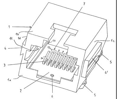
Figures 1 and 2 show two three-dimensional views of a
female connector according to the invention with a
holding element 1 which forms a holder 11 with the same
shape as conventional RJ45 female connectors, for a
plug. Figures 3 and 4 show two different installation
positions of this female connector on a base printed
circuit board 9.
The holding element 1 has an essentially cuboid basic
shape with a bottom surface la and top surface 1b, and
two parallel side surfaces lc, ld. The rearward area 1e
in the present case is inclined or designed in a prism
shape, in order to make it possible to mount the
connecting element on a base printed circuit board in
various installation positions (Figures 3 and 4).
The compensation printed circuit board 2 according to
the invention is arranged within the holding element 1,
in this case in the area of the bottom surface la. The
compensation printed circuit board 2 can, where
appropriate, replace the bottom surface la. Sprung
contact elements 3 which are bent in a hook shape are
located on the compensation printed circuit board 2,
and their contact surfaces 3a project into the holder
11 and are oriented such that they point obliquely to
the rear and away from the insertion opening for the
plug. As is shown in Figure 3, the length L of the
contact elements 3 is only a fraction (in this case
approximately one quarter) of the length of the female
connector measured in the insertion direction E, while
CA 02463792 2004-04-15
- 6 -
the contact elements according to the prior art
generally extend over the entire length of the female
connector. A compensation circuit 13 is also located on
the compensation printed circuit board 2, although it
is only indicated here. Figures 6a, b show one example
of a compensation circuit 13. The compensation circuit
13 connects the contact elements 3 to connections 7
which in this case are in the form of pins, and by
means of which electrical contact is made with the base
printed circuit board 9 in the application illustrated
in Figures 3, 4. The compensation printed circuit board
2 is guided in two side grooves 10 in the holding
element 1 and is fixed by means of a latching
connection 6, comprising a cut-out in the compensation
printed circuit board 2 and a latching tab in the
bottom surface. This ensures that the female connector
can be assembled easily'. The holding element is
preferably integral, in particular an injection-moulded
or die-cast part. The female connector may also have
additional metallic screening, for example surrounding
the holding element.
The holding element 1 has mounting elements 5 in the
form of latching tabs or feet, which are used for
mounting in corresponding cut-outs 14 in the base
printed circuit board 9. The mounting elements 5 are
arranged in different orientations with respect to the
bottom surface la, so that the female connector can be
installed in different positions. This allows the
insertion direction E of the plug to be matched to the
requirements on the installation side, for example
parallel ( Figure 3 ) or at an angle a ( Figure 4 ) to the
bottom surface 1a, which is generally aligned parallel
to the wall that holds the connecting socket.
A connecting strip 8, for example also in the form of a
connecting block, is connected to the base printed
circuit board 9 and, in this application, is used for
permanent connection of lines of a data cable, which is
CA 02463792 2004-04-15
generally laid such that it is stationary. The
electrical contact with the corresponding contact
element 3 within the female connector is made via line
connections, which are not shown, on the base printed
circuit board 9 and via the connections 7. The base
printed circuit board 9 may also have a further
compensation circuit in order to compensate for
crosstalk that occurs outside the female connector.
At the side, the holding element 1 has coupling
elements 4, 4' which are matched to one another, in
this case in the form of an undercut rail or a
dovetail-shaped attachment, which is used for coupling
two or more female connectors to one another. Figure 5
shows one example of a female connector arrangement
such as this.
Standard elements, for example double-sided FR4 printed
circuit board, may be used for the compensation printed
circuit board and for the base printed circuit board.
Figures 6a, b show one example of a compensation
circuit 13. The illustrations show the upper face and
lower face of the compensation printed circuit board 2
with the respective electronic components, in this case
line elements 15 and capacitors 16. In the present
case, one decoupling capacitor 16 is in each case
located between the line elements, which are associated
with the pin pairs 1/3, 3/5, 4/6 and 6/8. Typical
values for these capacitances are, for example, 0.81 pF
for the pairs 1/3 and 6/8, and 0.92 pF for the pairs
3/5 and 4/6 (at 250 MHz in each case). Considerably
higher capacitances and/or more complex circuits are
used for the previously known compensation circuits on
the printed circuit board, for example a decoupling
circuit with the following capacitances between the
stated pin pairs: pair 6/4: 2.1 pF; pair 5/3: 2.14 pF;
pair 6/8: 1.84 pF; pair 3/8: 1.4 pF; pair 1/3: 0.58 pF.
CA 02463792 2004-04-15
The dimensions of the compensation printed circuit
board 2 are matched to the size of the female
connector, and in the present case they are about 17 mm
long and 12 mm wide.