Sélection de la langue

Search

Sommaire du brevet 2463792 

Énoncé de désistement de responsabilité concernant l'information provenant de tiers

Une partie des informations de ce site Web a été fournie par des sources externes. Le gouvernement du Canada n'assume aucune responsabilité concernant la précision, l'actualité ou la fiabilité des informations fournies par les sources externes. Les utilisateurs qui désirent employer cette information devraient consulter directement la source des informations. Le contenu fourni par les sources externes n'est pas assujetti aux exigences sur les langues officielles, la protection des renseignements personnels et l'accessibilité.

Disponibilité de l'Abrégé et des Revendications

L'apparition de différences dans le texte et l'image des Revendications et de l'Abrégé dépend du moment auquel le document est publié. Les textes des Revendications et de l'Abrégé sont affichés :

  • lorsque la demande peut être examinée par le public;
  • lorsque le brevet est émis (délivrance).
(12) Brevet: (11) CA 2463792
(54) Titre français: CONNECTEUR FEMELLE ET DOUILLE DE CONNEXION POUR LA PRODUCTION D'UNE CONNEXION DE LIGNE DE DONNEES DE GRANDE PUISSANCE
(54) Titre anglais: FEMALE CONNECTOR AND CONNECTING SOCKET FOR PRODUCING A HIGH-POWER DATA LINE CONNECTION
Statut: Périmé et au-delà du délai pour l’annulation
Données bibliographiques
(51) Classification internationale des brevets (CIB):
  • H01R 13/66 (2006.01)
  • H01R 13/514 (2006.01)
  • H01R 24/58 (2011.01)
(72) Inventeurs :
  • EBERLE, ANDREAS (Liechtenstein)
  • NEFF, FRANZ (Liechtenstein)
  • DAUBA, HERBERT (Allemagne)
(73) Titulaires :
  • SETEC NETZWERKE AG
(71) Demandeurs :
  • SETEC NETZWERKE AG (Liechtenstein)
(74) Agent: GOWLING WLG (CANADA) LLP
(74) Co-agent:
(45) Délivré: 2010-08-03
(86) Date de dépôt PCT: 2002-10-23
(87) Mise à la disponibilité du public: 2003-05-08
Requête d'examen: 2007-08-08
Licence disponible: S.O.
Cédé au domaine public: S.O.
(25) Langue des documents déposés: Anglais

Traité de coopération en matière de brevets (PCT): Oui
(86) Numéro de la demande PCT: PCT/EP2002/011842
(87) Numéro de publication internationale PCT: EP2002011842
(85) Entrée nationale: 2004-04-15

(30) Données de priorité de la demande:
Numéro de la demande Pays / territoire Date
01125756.5 (Office Européen des Brevets (OEB)) 2001-10-29

Abrégés

Abrégé français

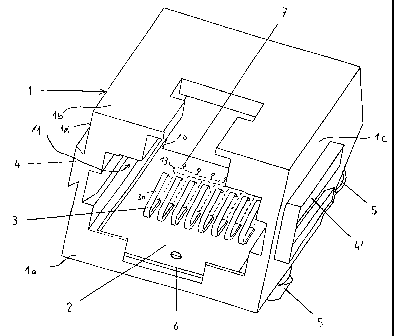
Prise femelle qui comporte un élément récepteur (1) pour une fiche mâle d'un câble de données comprenant une pluralité de lignes, et une pluralité d'éléments de contact (3) électriquement conducteurs qui, en cas d'utilisation, se trouvent en contact avec des lignes d'une fiche mâle introduite dans l'élément récepteur (1). Selon la présente invention, une carte de circuit imprimé de compensation (2) dotée d'un circuit de compensation (13) et placée dans l'élément récepteur (1) est destinée à réduire les influences perturbatrices, en particulier la diaphonie, les éléments de contacts (3) étant fixés sur ladite carte. La présente invention concerne en outre une prise de courant comportant une prise femelle de ce type.


Abrégé anglais


The invention relates to a socket comprising a receiving element (1) for the
plug of a data cable, comprising a plurality of lines, and a plurality of
electrically conductive contact elements (3) which enter into contact with
lines of a plug inserted into the receiving element (1) when used. According
to the invention, a compensation printed board (2) with a compensation circuit
(13) is provided in order to reduce disturbing influences, especially cross-
talk, and is arranged inside the receiving element (1), whereby the contact
elements (3) are fixed thereto. The invention also relates to a connector
comprising said socket.

Revendications

Note : Les revendications sont présentées dans la langue officielle dans laquelle elles ont été soumises.


-9-
1. Connecting socket for producing a high-power data
line connection between lines of a data cable, which is
laid permanently, and of a further data cable,
comprising at least one female connector, a base
printed circuit board (9) on which the at least one
female connector is mounted, and at least one
connecting strip (8) with contact elements for
connection of lines of the stationary data cable, with
the female connector having a holding element (1) for a
male connector of a data cable and having two or more
electrically conductive contact elements (3) which, in
use, make contact with lines of a male connector which
is inserted into the holding element (1), and with the
base printed circuit board (9) having line elements for
producing an electrically conductive connection between
contact elements of the connecting strip (8) and the
contact elements (3) of the female connector
characterized in that a compensation printed circuit
board (2) is arranged within the holding element (1) of
the female connector and contains a compensation
circuit (13) in order to reduce interference
influences, in particular crosstalk, and on which the
contact elements (3) are mounted, and in that the base
printed circuit board (9) contains a further
compensation circuit in order to reduce interference
influences.
2. Connecting socket according to Claim 1,
characterized in that in use, the compensation printed
circuit board (2) is located in the immediate physical
vicinity of a male connector, which is inserted into
the female connector on a data cable.
3. Connecting socket according to Claim 1 or 2,
characterized in that the holding element (1) has a
bottom surface (1a), a top surface (1b) and two side
surfaces (1c, 1d) which form a holder for a male

-10-
connector, with the compensation printed circuit board
(2) being arranged parallel to the bottom surface (1a)
of the holding element, and preferably in its immediate
physical vicinity.
4. Connecting socket according to Claim 3,
characterized in that the compensation printed circuit
board (2) is guided in grooves (10), and is preferably
fixed by means of a latching mechanism (6) within the
holding element (1).
5. Connecting socket according to one of the
preceding claims, characterized by at least one
mounting element (5), by means of which the female
connector can be mounted on a base printed circuit
board (9) such that the male connector can be inserted
into the holding element (1) parallel to the base
printed circuit board (9), or at a predetermined angle
(.alpha.) to it.
6. Connecting socket according to one of the
preceding claims, characterized in that the contact
elements (3) are curved like hooks and have a contact
surface (3a) which is oriented at an acute angle to the
compensation printed circuit board (2).
7. Connecting socket according to one of the
preceding claims, characterized in that the length of
the contact elements (3) is between 3 and 8 mm,
preferably between 4 and 6 mm.
8. Connecting socket according to one of the
preceding claims, characterized by at least one
coupling element (4, 4') which is arranged on the side
of the holding element (1) and by means of which at
least two female connectors can be preferably
detachably connected to form a common arrangement.

-11-
9. Connecting socket according to one of the
preceding claims, characterized in that the female
connector is mounted on the base printed circuit board
(9) such that the male connector can be inserted into
the holding element (1) parallel to the base printed
circuit board (9) or at a predetermined angle (.alpha.) to
it.
10. Connecting socket according to one of the
preceding claims, characterized by a housing which
covers the base printed circuit board (9) and the at
least one female connector, and has at least one
aperture for insertion of a male connector into the at
least one female connector.
11. Use of a female connector having a holding element
(1) for a male connector on a data cable, which has two
or more lines, having two or more electrically
conductive contact elements (3) which, in the
application, make contact with lines of a male
connector which is inserted into the holding element
(1), and having a compensation printed circuit board
(2), which contains a compensation circuit (13) for
reducing interference influences, in particular the
crosstalk, is arranged within the holding element (1)
and to which the contact elements (3) are attached in
order to produce a connecting socket according to one
of the preceding claims.

Description

Note : Les descriptions sont présentées dans la langue officielle dans laquelle elles ont été soumises.


CA 02463792 2004-04-15
Female connector and connecting socket for producing a
high-power data line connection
The invention relates to a female connector and
connecting socket for producing a high-power data line
connection to such a female connector according to
Claims 1 and 9.
In order to produce a data line connection from a
server to a terminal (channel) or between the
corresponding connecting socket (link) with a high data
transmission capacity, all the components of the
channel or link, in particular the data cables and
connecting sockets, have to satisfy specific minimum
requirements relating to their transmission
characteristics. The components are subdivided on the
basis of their transmission characteristics into
various categories of which, at the moment, categories
5, 5e and 6 are of particular interest. It is planned
to standardize the specifications for components in the
relevant categories. On the basis of a standardization
proposal such as this, cables in categories 5, 5e and 6
have to suppress the near end crosstalk or NEXT by
32.3, 35.3 or 44.3 dB at 100 MHz. For connecting
sockets of categories 5, 5e and 6, values of 40, 43 and
54 dB apply for NEXT losses at 100 MHz. The
requirements for classes 5, 5e and 6 can be satisfied
relatively well at the moment for cables, but no
satisfactory solution exists for connecting sockets,
particularly those in category 6.
Connecting sockets normally have at least one female
connector, for example an RJ45 female connector, with a
holding element for the plug of a data cable and two or
more elongated contact elements, which are bent in a
hook shape, extend over the majority of the length of
the holding element and, during use, make contact with
the lines of the data cable, or the corresponding
contact elements on the plug. The female connector is

CA 02463792 2004-04-15
- 2 -
mounted on a base printed circuit board, which contains
line connections to a connecting strip for a further
data cable, which is generally stationary. One end of
the hook-shaped contact elements of the female
connector is in each case passed out of the holding
element and is soldered directly to the base printed
circuit board, or to a line connection on it. In known
designs, the electrically conductive components are
located in the immediate .physical vicinity of one
another without any screening, and interfere with one
another. RJ45 female connectors have 8 contact elements
which are located alongside one another, for the 4
pairs of lines in the corresponding data cables. One
line pair is in each case associated with the contact
elements 112, 4/5 and 7/8, while a further line pair is
connected to the contact elements 3 and 6. Because of
this physical arrangement, the interference between the
pairs 3/6 and 4/5 is particularly severe.
In order to reduce interference, it is known for the
base printed circuit board to be equipped with a
compensation circuit which decouples individual lines
or line pairs from one another, fox example
capacitively. Connecting sockets with such compensation
circuits generally comply with the category 5 or 5e
requirements. However, an improvement by 11 dB at
100 MHz is required for the jump to category 6, and
this has not yet been achieved with the described
design.
A female connector with a holding element and a printed
circuit board integrated in it is known from
US 6,190,211. A compensation circuit is located on the
printed circuit board, in order to reduce interference.
The invention is thus based on the object of specifying
a female connector and a connecting socket with
improved transmission characteristics. The female
connector should preferably have the same geometry as

CA 02463792 2004-04-15
- 3 -
female connectors that are already in use, in
particular in accordance with RJ45, in order to be
compatible with conventional standard plugs.
The object is achieved by a female connector having the
features of Claim 1 and by a connecting socket having
the features of Claim 9. Advantageous developments of
the invention can be found in the dependent claims, in
the description and in the drawings.
The invention is based on the surprising knowledge that
even structures of less than 1/10 of the wavelength of
the relevant signals have an influence on the mutual
interference. Moving the compensation circuit from the
base printed circuit board into the immediate physical
vicinity of the contact elements of the female
connector leads to considerably better compensation, in
particular for the NEXT values. This effect is
reinforced by shortening the length of the contact
elements or of the signal paths from the contact
elements of the plug to the compensation circuit, or to
the connections of a further cable. The signals are
provided with compensation before they leave the female
connector, and need not be corrected, or can be
corrected in a less complex manner, on the base printed
circuit board.
According to the invention, the contact elements of a
female connector are attached to a compensation printed
circuit board, which contains a compensation circuit in
order to reduce interference influences, in particular
crosstalk influences, between lines, and which is
arranged within the holding element for the plug. The
contact elements in the female connector may be very
short since they extend only from the contact elements
of the plug to the compensation printed circuit board,
and need not be passed out of the female connector or
holding element, as in the case of the prior art. The
strength of the mutual interference between the signal

CA 02463792 2004-04-15
- 4 -
paths, in particular the mutual crosstalk, is reduced.
Finally, the compensation circuit on the compensation
printed circuit board may be simplified, for example by
using capacitors with smaller capacitances.
The compensation printed circuit board may be
integrated in any desired female connectors whose
holding element is particularly matched to plugs with a
form that is known per se.. This avoids compatibility
problems when changing to category 6 components.
Holding elements and female connectors which correspond
to the RJ45 shape are preferably used. The compensation
printed circuit board extends, for example, over the
bottom surface of the holding element or forms the
bottom surface, and is removable. Mounting elements are
preferably provided for mounting on the base printed
circuit board, and, in a particularly preferably form,
they allow mounting in various positions relative to
it.
In addition to at least one female connector according
to the invention, the connecting 'socket has a base
printed circuit board and a connecting strip. Further
elements may also be provided, for example in order to
form a preferably screened housing. The housing may be
designed in a known manner, for example according to
EP-A 0928052.
Exemplary embodiments of the invention will be
described in the following text and are illustrated in
the drawings in which, purely schematically:
Figures l, 2 show a female connector according to the
invention in a view obliquely from the
front and from the rear, respectively;
Figures 3, 4 show a section through a connecting
socket according to the invention with a

CA 02463792 2004-04-15
- 5 -
female connector in two different
installation positions;
Figure 5 shows two female connectors coupled to
one another;
Figures 6a,b show an example of a compensation
circuit.
Figures 1 and 2 show two three-dimensional views of a
female connector according to the invention with a
holding element 1 which forms a holder 11 with the same
shape as conventional RJ45 female connectors, for a
plug. Figures 3 and 4 show two different installation
positions of this female connector on a base printed
circuit board 9.
The holding element 1 has an essentially cuboid basic
shape with a bottom surface la and top surface 1b, and
two parallel side surfaces lc, ld. The rearward area 1e
in the present case is inclined or designed in a prism
shape, in order to make it possible to mount the
connecting element on a base printed circuit board in
various installation positions (Figures 3 and 4).
The compensation printed circuit board 2 according to
the invention is arranged within the holding element 1,
in this case in the area of the bottom surface la. The
compensation printed circuit board 2 can, where
appropriate, replace the bottom surface la. Sprung
contact elements 3 which are bent in a hook shape are
located on the compensation printed circuit board 2,
and their contact surfaces 3a project into the holder
11 and are oriented such that they point obliquely to
the rear and away from the insertion opening for the
plug. As is shown in Figure 3, the length L of the
contact elements 3 is only a fraction (in this case
approximately one quarter) of the length of the female
connector measured in the insertion direction E, while

CA 02463792 2004-04-15
- 6 -
the contact elements according to the prior art
generally extend over the entire length of the female
connector. A compensation circuit 13 is also located on
the compensation printed circuit board 2, although it
is only indicated here. Figures 6a, b show one example
of a compensation circuit 13. The compensation circuit
13 connects the contact elements 3 to connections 7
which in this case are in the form of pins, and by
means of which electrical contact is made with the base
printed circuit board 9 in the application illustrated
in Figures 3, 4. The compensation printed circuit board
2 is guided in two side grooves 10 in the holding
element 1 and is fixed by means of a latching
connection 6, comprising a cut-out in the compensation
printed circuit board 2 and a latching tab in the
bottom surface. This ensures that the female connector
can be assembled easily'. The holding element is
preferably integral, in particular an injection-moulded
or die-cast part. The female connector may also have
additional metallic screening, for example surrounding
the holding element.
The holding element 1 has mounting elements 5 in the
form of latching tabs or feet, which are used for
mounting in corresponding cut-outs 14 in the base
printed circuit board 9. The mounting elements 5 are
arranged in different orientations with respect to the
bottom surface la, so that the female connector can be
installed in different positions. This allows the
insertion direction E of the plug to be matched to the
requirements on the installation side, for example
parallel ( Figure 3 ) or at an angle a ( Figure 4 ) to the
bottom surface 1a, which is generally aligned parallel
to the wall that holds the connecting socket.
A connecting strip 8, for example also in the form of a
connecting block, is connected to the base printed
circuit board 9 and, in this application, is used for
permanent connection of lines of a data cable, which is

CA 02463792 2004-04-15
generally laid such that it is stationary. The
electrical contact with the corresponding contact
element 3 within the female connector is made via line
connections, which are not shown, on the base printed
circuit board 9 and via the connections 7. The base
printed circuit board 9 may also have a further
compensation circuit in order to compensate for
crosstalk that occurs outside the female connector.
At the side, the holding element 1 has coupling
elements 4, 4' which are matched to one another, in
this case in the form of an undercut rail or a
dovetail-shaped attachment, which is used for coupling
two or more female connectors to one another. Figure 5
shows one example of a female connector arrangement
such as this.
Standard elements, for example double-sided FR4 printed
circuit board, may be used for the compensation printed
circuit board and for the base printed circuit board.
Figures 6a, b show one example of a compensation
circuit 13. The illustrations show the upper face and
lower face of the compensation printed circuit board 2
with the respective electronic components, in this case
line elements 15 and capacitors 16. In the present
case, one decoupling capacitor 16 is in each case
located between the line elements, which are associated
with the pin pairs 1/3, 3/5, 4/6 and 6/8. Typical
values for these capacitances are, for example, 0.81 pF
for the pairs 1/3 and 6/8, and 0.92 pF for the pairs
3/5 and 4/6 (at 250 MHz in each case). Considerably
higher capacitances and/or more complex circuits are
used for the previously known compensation circuits on
the printed circuit board, for example a decoupling
circuit with the following capacitances between the
stated pin pairs: pair 6/4: 2.1 pF; pair 5/3: 2.14 pF;
pair 6/8: 1.84 pF; pair 3/8: 1.4 pF; pair 1/3: 0.58 pF.

CA 02463792 2004-04-15
The dimensions of the compensation printed circuit
board 2 are matched to the size of the female
connector, and in the present case they are about 17 mm
long and 12 mm wide.

Dessin représentatif
Une figure unique qui représente un dessin illustrant l'invention.
États administratifs

2024-08-01 : Dans le cadre de la transition vers les Brevets de nouvelle génération (BNG), la base de données sur les brevets canadiens (BDBC) contient désormais un Historique d'événement plus détaillé, qui reproduit le Journal des événements de notre nouvelle solution interne.

Veuillez noter que les événements débutant par « Inactive : » se réfèrent à des événements qui ne sont plus utilisés dans notre nouvelle solution interne.

Pour une meilleure compréhension de l'état de la demande ou brevet qui figure sur cette page, la rubrique Mise en garde , et les descriptions de Brevet , Historique d'événement , Taxes périodiques et Historique des paiements devraient être consultées.

Historique d'événement

Description Date
Représentant commun nommé 2019-10-30
Le délai pour l'annulation est expiré 2019-10-23
Lettre envoyée 2018-10-23
Requête pour le changement d'adresse ou de mode de correspondance reçue 2018-01-10
Inactive : CIB désactivée 2011-07-29
Inactive : CIB du SCB 2011-01-10
Inactive : CIB expirée 2011-01-01
Accordé par délivrance 2010-08-03
Inactive : Page couverture publiée 2010-08-02
Préoctroi 2010-05-14
Inactive : Taxe finale reçue 2010-05-14
Un avis d'acceptation est envoyé 2010-01-05
Inactive : Lettre officielle 2010-01-05
Lettre envoyée 2010-01-05
Un avis d'acceptation est envoyé 2010-01-05
Inactive : Approuvée aux fins d'acceptation (AFA) 2009-12-21
Modification reçue - modification volontaire 2009-09-28
Inactive : Dem. de l'examinateur par.30(2) Règles 2009-05-28
Modification reçue - modification volontaire 2007-10-11
Lettre envoyée 2007-08-22
Requête d'examen reçue 2007-08-08
Exigences pour une requête d'examen - jugée conforme 2007-08-08
Toutes les exigences pour l'examen - jugée conforme 2007-08-08
Lettre envoyée 2005-05-09
Inactive : Correspondance - Transfert 2005-04-20
Inactive : Transfert individuel 2005-04-07
Inactive : IPRP reçu 2004-06-25
Inactive : Page couverture publiée 2004-06-23
Inactive : Lettre de courtoisie - Preuve 2004-06-15
Inactive : Notice - Entrée phase nat. - Pas de RE 2004-06-11
Demande reçue - PCT 2004-05-13
Exigences pour l'entrée dans la phase nationale - jugée conforme 2004-04-15
Demande publiée (accessible au public) 2003-05-08

Historique d'abandonnement

Il n'y a pas d'historique d'abandonnement

Taxes périodiques

Le dernier paiement a été reçu le 2009-09-24

Avis : Si le paiement en totalité n'a pas été reçu au plus tard à la date indiquée, une taxe supplémentaire peut être imposée, soit une des taxes suivantes :

  • taxe de rétablissement ;
  • taxe pour paiement en souffrance ; ou
  • taxe additionnelle pour le renversement d'une péremption réputée.

Les taxes sur les brevets sont ajustées au 1er janvier de chaque année. Les montants ci-dessus sont les montants actuels s'ils sont reçus au plus tard le 31 décembre de l'année en cours.
Veuillez vous référer à la page web des taxes sur les brevets de l'OPIC pour voir tous les montants actuels des taxes.

Titulaires au dossier

Les titulaires actuels et antérieures au dossier sont affichés en ordre alphabétique.

Titulaires actuels au dossier
SETEC NETZWERKE AG
Titulaires antérieures au dossier
ANDREAS EBERLE
FRANZ NEFF
HERBERT DAUBA
Les propriétaires antérieurs qui ne figurent pas dans la liste des « Propriétaires au dossier » apparaîtront dans d'autres documents au dossier.
Documents

Pour visionner les fichiers sélectionnés, entrer le code reCAPTCHA :


Pour visualiser une image, cliquer sur un lien dans la colonne description du document. Pour télécharger l'image (les images), cliquer l'une ou plusieurs cases à cocher dans la première colonne et ensuite cliquer sur le bouton "Télécharger sélection en format PDF (archive Zip)" ou le bouton "Télécharger sélection (en un fichier PDF fusionné)".

Liste des documents de brevet publiés et non publiés sur la BDBC .

Si vous avez des difficultés à accéder au contenu, veuillez communiquer avec le Centre de services à la clientèle au 1-866-997-1936, ou envoyer un courriel au Centre de service à la clientèle de l'OPIC.


Description du
Document 
Date
(aaaa-mm-jj) 
Nombre de pages   Taille de l'image (Ko) 
Dessins 2004-04-14 6 93
Revendications 2004-04-14 3 121
Abrégé 2004-04-14 2 89
Description 2004-04-14 8 342
Dessin représentatif 2004-04-14 1 23
Description 2009-09-27 9 369
Revendications 2009-09-27 4 124
Dessin représentatif 2010-07-20 1 15
Avis d'entree dans la phase nationale 2004-06-10 1 192
Rappel de taxe de maintien due 2004-06-24 1 111
Demande de preuve ou de transfert manquant 2005-04-17 1 100
Courtoisie - Certificat d'enregistrement (document(s) connexe(s)) 2005-05-08 1 104
Rappel - requête d'examen 2007-06-26 1 118
Accusé de réception de la requête d'examen 2007-08-21 1 177
Avis du commissaire - Demande jugée acceptable 2010-01-04 1 162
Avis concernant la taxe de maintien 2018-12-03 1 183
PCT 2004-04-14 14 637
Correspondance 2004-06-10 1 27
PCT 2004-04-15 4 134
Correspondance 2010-01-04 1 32
Correspondance 2010-05-13 2 49