Note: Descriptions are shown in the official language in which they were submitted.
CA 02798105 2014-12-31
75089-111
1
Circuit for the Clocking of an FPGA
The present invention concerns a circuit for the clocking of an FPGA. FPGAs
with low
power consumption are known. In measurement technology FPGAs can be
employed, by way of example, which comprise a current load of around 80 pA. On
the other hand, applications in measurement technology require, by way of
example,
precise clocking, i.e. the deviation from the fundamental frequency should not
account for more than +1- 0.1 % or +1- 0.2 % as the case may be. Such precise
clocking with low power consumption cannot be readily provided by commercially
available oscillators. It would be possible to generate a very precise clock
signal with
a PLL circuit integrated into the FPGA, which produces a higher clock
frequency,
which is based on an external reference clock. However, such PLL-circuits have
the
disadvantage that their power consumption is too large. As they are, they
account for
a typical power consumption of around 1 mA, i.e. about 12 times the above
mentioned power consumption of the FPGA on its own. This makes the provision
of a
system clock by means of an integrated PLL-circuit unattractive. It is
therefore the
object of the present invention to provide a circuit, which overcomes the
disadvantages of the prior art.
According to an aspect of the invention, there is provided a circuit
comprising: an
FPGA, which comprises an FLL-circuit; a reference clock of a first frequency,
or a
reference clock input for the reception of a signal of a reference clock of a
first
frequency; a digitally controlled oscillator, which outputs a clocking signal
for said
FPGA, wherein: the FLL-circuit is designed in order to register a first number
of clock
signals from the digitally controlled oscillator during a second number of
periods of
the reference clock; the first number is larger than the second number, and,
in order
to give out a feedback signal to control the ratio between the first number
and the
second number, as the feedback signal acts on the frequency of the digitally
controlled oscillator; the frequency of the digitally controlled oscillator is
controlled via
at least one resistance value, on which the feedback signal acts; the
resistance value
is adjustable via a series of individual resistors, which, for the reduction
of the
CA 02798105 2016-01-07
75089-111
la
resistance, can be selectively bypassed with respect to ground, at least in
part; the
series of the resistors that can be selectively bypassed account for, not more
than
10% of the total value of the resistance; the series of resistors that can be
bypassed
comprises at least 10 individual resistors; and the frequency of the digitally
controlled
oscillator is, due to the feedback signal, not variable by more than 5%.
The inventive circuit comprises an FPGA, which comprises an FLL-circuit; a
reference clock of a first frequency, or a reference clock input for the
reception of a
signal of a reference clock of a first frequency;
a digitally controlled oscillator, which outputs a clocking signal for the
FPGA, wherein
the FLL-circuit is designed in order to register a first number of clock
signals from the
digitally controlled oscillator during a second number of periods of the
reference
clock, wherein the first number is larger than the
CA 02798105 2012-10-31
2
second number, and, in order to give out 'a feedback signal to control the
ratio
between the first number and the second number, as the feedback signal
acts on the frequency of the digitally controlled oscillator.
In a further embodiment of the invention, the frequency of the digitally
controlled oscillator is, due to the feedback signal, not variable by more
than
5%, in particular by not more than 2% and preferably by not more than 1%.
In a presently preferred embodiment of the invention, the number of clocking
signals from the digitally controlled oscillator is registered during one
period of
the reference clock. In this case, the second number is then 1. Evidently, the
second number can also take on another value, such as 2, 3, 4, or 5, for
example.
The ratio between the first number and the second number comprises a
preset or presettable desired value, which is larger than 10:1, preferably
larger than 100:1 and especially preferably not smaller than 500:1.
The frequency of the digitally controlled oscillator is controlled, according
to
an embodiment of the invention, via at least one resistance value, on which
the feedback signal acts.
In an embodiment of the invention, the resistance value is adjustable via a
series of individual resistors, which, for the reduction of the resistance,
can
beselectively bypassed with respect to ground, at least in part. The series of
the resistors that can beselectivelybypassed,account for, by way of example,
not more than 20%, and in particular not more than 10% of the total value of
the resistance. The series of resistors that can be bypassed, by way of
example, comprises at least 5, in particular at least 10 and preferably at
least
20 individual resistors.
CA 02798105 2012-10-31
3
The series of individual resistors, according to a further embodiment of the
invention, comprises at least one resistive element with a variable resistive
value. The variable resistance value can thereby in particular be varied
between a minimum value and a maximum value, wherein, in particular for
the case where the resistive elements that can be bypassed all comprise the
same resistive value, the maximum value equals the resistive value of the
resistive elements that can be bypassed. The minimum value is as small as
possible; in particular, it accounts for less than 5%, preferably less than 2%
and especially preferably less than 1% of the maximum value. In this way,
the total value of the resistance, which controls the digitally controlled
oscillator, can be adjusted in an almost continuous way by bypassing select
resistive elements and adjusting the in-between values by means of the
variable resistive element.
R total = ,Rn * R intifin :dual + a * R int-filth:tura
Wherein Ro is a fixed base resistance value that accounts for, by way of
example, 80% or more of the total resistance, and wherein Rindividual is the
resistive value of the individual resistive elements that can be bypassed,
That is
R total ¨ 0
R f nthuidu ai N
Wherein N ¨ 1 is the number of the resistors that can be bypassed,
Wherein i = 0, 1, ,N -1, and
Wherein a = 0 ... 1.
The parameter 'i'designates then the number of individual resistors that
contribute to the total resistance value, while the factor 'a' designates the
effective contribution of the continuously adjustable resistive element as a
fraction of its maximum resistance Rindividual=
For the case where no variable resistive element is provided, then:
CA 02798105 2012-10-31
4
Rtotal = 4- * Rindividual
applies in particular, where:
Rroral ¨ Ro
Rfncliviclual N
wherein N is the number of resistors that can be bypassed, and
wherein i = 0, 1, ... N.
In a further embodiment of the invention, the resistance value is adjustable
via a network of at least partially bypassable, individual resistors, wherein
the
network comprises resistors arranged in parallel and in series.
In a further embodiment of the invention, the first frequency of the reference
clockis not less than 10 Hz, in particular not less than 50 Hz, and especially
preferably not less than 100 Hz. The frequency of the reference clock is,
according to this further embodiment of the invention, not more than 1 kHz, in
particular not more than 500 Hz, and especially preferably not more than 250
Hz.
The FLL-circuit, according to a further embodiment of the invention, can
furthermore comprise a scaling component for the output of a third frequency
f3, wherein the third frequency f3 is given as a ratio, N:M, to the second
frequency f2, so that M * F3 = N * f2 =
The invention is described with the help of the illustrative embodiments in
the
following figures.
They show:
Fig. 1: a schematic illustration of the inventive circuit;
Fig. 2: a block circuit diagram for the control of a digitally controlled
oscillator,
by means of a chain of resistors; and
CA 02798105 2014-12-31
' 75089-111
Fig. 3: a block circuit diagram of the circuit, according to the invention,
with
control of a digitally controlled oscillator by means of an FPGA by means of a
chain of resistors.
5 The circuit 1 illustrated in Fig. 1 comprises an FPGA 2, a digitally
controllable
oscillator 3, a reference clock 4 with a low clock frequency, and an FLL-
circuit
5 (Frequency Locked Loop), wherein the FLL-circuit receives on the one hand
the low frequency inputfrom the reference clock 4 and the high frequency
inputfrom the digitally controlled oscillator 3. The reference clock and the
digitally controlled oscillator are external components that are connected to
the FPGA. Thus, the FLL-circuit controls the higher frequency output of the
digitally controlled oscillator with respect to the lower frequency signal of
the
reference clockby means of a countingmethod. In this, an edge triggered
counting of the higher frequency signal occurs during the window of time
preset by the reference clock, and this is then compared with a desired value.
The frequency of the digitally controlled oscillator is increased or decreased
depending on the result of the comparison. The digitally controlled oscillator
is an external, resistor controlled oscillator, with low energy consumption in
the presently preferred embodiment of the invention, by way of example, the
LTC 6906. This digitally controlled oscillator can generate a signal between
10 kHz and 1 MHz, wherein the current drawn, at a supply voltage of about
3.15 V and a signal frequency of around 300 kHz, is on the order of 20 pA.
The pin configuration of the digitally controlled oscillator 3 is illustrated
in
detail in Fig. 2. The pins of the digitally controlled oscillator 3 are used
in the
following way:
3-1: clock with a frequency of between 10 kHz and 1 MHz
3-2: circuit ground
3-3: voltage divider
3-4: control input
3 -6: voltage supply input
CA 02798105 2014-12-31
75089-111
6
The voltage divider input 3-3 is grounded, so that the clock 3-1 outputs an
unaltered signal frequency. A series circuit of resistive elements is provided
at the control input 3-4, which is chosen so that a desired value between
about 300 kHz and 330 kHz, in particular about 314 kHz, is outputted as a
clock signal. The chain of resistors comprises a number of resistive elements
=that cannot be bypassed and, when taken together, comprise a resistive value
of about 318 ka To this is connected a chain of 22, 680 0,resistors that can
be bypassed. The resistive elements can be bypassed by means of the
FPGA 2, wherein by making a connection to one of the control pins Control 0
to Control 21, a portion of the resistor chain is bypassed with respect to
ground. It is possible, in this way, to reduce the total of value of the
effective
resistance, in discrete steps, up to about 5%. The desired frequency is
reached, under ideal conditions, at 97.5% of the total value, so that
deviations
in the value of the resistance or in the oscillator due to, by way of example,
temperature changes or because of manufacturing tolerances, the frequency
can be increased or decreased by making a connection with another control
pin.Whether or not the control pin that is presently chosen is too high or
low, is
determined from the comparison of the desired value to the clock signal of the
digitally controlled oscillator during one period of the reference clock.
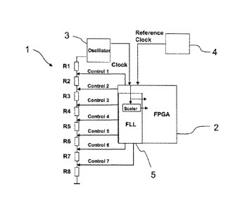
Fig. 3 shows an overview, wherein for the sake of simplicity, only 7 control
pins, control 1 to control 7, which can bypass part of the resistor chain, are
illustrated.
By way of example, the chain of resistors can be bypassed at the control pin
Control 4 as an initial default value, wherein, depending on deviations from
the desired value to the countedclock signal of the digitally controlled
oscillator, another control pin is activated in order to increase or lower the
clock frequency.
CA 02798105 2012-10-31
7
The energy consumption for the control of the control nodes and the FLL-
circuit accounts for about 10pA (at a voltage supply of 3.15 V), so that the
total current draw for the generation of a rapid and acceptably precise
clocking is around 30 pA at the present supply voltage. This represents a
decrease in the power consumption vis-a-vis the current PLL-circuits, which
comprise a current draw of about 1 mA at the present supply voltage, by a
factor of more than 30.
By nature, switching between discrete resistance values implies the result
that the clock frequency of the oscillator will comprise a certain amount of
jitter if the frequency is not randomly achieved by a preset resistor
configuration. In case the jitter is undesirable, the resistor chain can
comprise
an additional variable resistor, whose value can be continuously controlled.
Furthermore, instead of a row of resistors with many resistive elements of
equal value,a resistance network can be employed, with parallel and series
resistive circuit elements, with which other incremental values can be formed
as whole number multiples of a resistive element.
Further embodiments and possible variations of the invention present
themselves for persons skilled in the art in the context of the present
disclosure without deviating from the core of the invention.