Sélection de la langue

Search

Sommaire du brevet 2798105 

Énoncé de désistement de responsabilité concernant l'information provenant de tiers

Une partie des informations de ce site Web a été fournie par des sources externes. Le gouvernement du Canada n'assume aucune responsabilité concernant la précision, l'actualité ou la fiabilité des informations fournies par les sources externes. Les utilisateurs qui désirent employer cette information devraient consulter directement la source des informations. Le contenu fourni par les sources externes n'est pas assujetti aux exigences sur les langues officielles, la protection des renseignements personnels et l'accessibilité.

Disponibilité de l'Abrégé et des Revendications

L'apparition de différences dans le texte et l'image des Revendications et de l'Abrégé dépend du moment auquel le document est publié. Les textes des Revendications et de l'Abrégé sont affichés :

  • lorsque la demande peut être examinée par le public;
  • lorsque le brevet est émis (délivrance).
(12) Brevet: (11) CA 2798105
(54) Titre français: CIRCUIT POUR CADENCER UN FPGA
(54) Titre anglais: CIRCUIT FOR THE CLOCKING OF AN FPGA
Statut: Accordé et délivré
Données bibliographiques
(51) Classification internationale des brevets (CIB):
  • H03K 19/177 (2020.01)
  • H03L 07/181 (2006.01)
(72) Inventeurs :
  • SCHLACHTER, MARC (Allemagne)
  • GIRARDEY, ROMUALD (France)
(73) Titulaires :
  • ENDRESS+HAUSER GMBH+CO.KG
(71) Demandeurs :
  • ENDRESS+HAUSER GMBH+CO.KG (Allemagne)
(74) Agent: SMART & BIGGAR LP
(74) Co-agent:
(45) Délivré: 2017-04-04
(86) Date de dépôt PCT: 2011-04-14
(87) Mise à la disponibilité du public: 2011-12-08
Requête d'examen: 2012-10-31
Licence disponible: S.O.
Cédé au domaine public: S.O.
(25) Langue des documents déposés: Anglais

Traité de coopération en matière de brevets (PCT): Oui
(86) Numéro de la demande PCT: PCT/EP2011/055947
(87) Numéro de publication internationale PCT: EP2011055947
(85) Entrée nationale: 2012-10-31

(30) Données de priorité de la demande:
Numéro de la demande Pays / territoire Date
102010028963.9 (Allemagne) 2010-05-12

Abrégés

Abrégé français

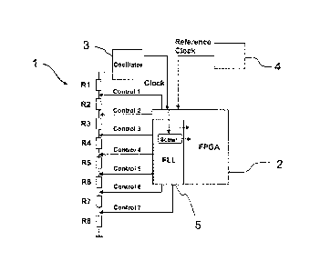
L'invention concerne un circuit (1), comprenant : un FPGA (2) (réseau prédiffusé programmable par l'utilisateur), qui présente une boucle FLL (5) (boucle à verrouillage de fréquence); un générateur d'horloge de référence (4) ayant une première fréquence, ou une entrée d'horloge de référence pour recevoir une horloge de référence de première fréquence; un oscillateur programmable (3) qui délivre un signal d'horloge pour le FPGA (2). La boucle FLL (5) est réalisée pour recenser un premier nombre de signaux d'horloge de l'oscillateur programmable (3) pendant un deuxième nombre de périodes de l'horloge de référence, le premier nombre étant supérieur au deuxième nombre, et pour délivrer un signal de rétroaction pour commander le rapport entre le premier nombre et le deuxième nombre, le signal de rétroaction agissant sur la fréquence de l'oscillateur programmable.


Abrégé anglais


Circuit1 comprising:an FPGA2, which comprises an FLL-circuit 5;a reference
clock 4 of a first frequency, or a reference clock input for the reception of
a
signal of a reference clock of a first frequency;a digitally controlled
oscillator
3, which outputs a clocking signal for the FPGA 2, wherein the FLL-circuit 5
is
designed in order to register a first number of clocking signals from the
digitally controlled oscillator4 during a second number of periods of the
reference clock, wherein the first number is larger than the second number,
and, in order to give out a feedback signal to control the ratio between the
first number and the second number, as the feedback signal acts on the
frequency of the digitally controlled oscillator.

Revendications

Note : Les revendications sont présentées dans la langue officielle dans laquelle elles ont été soumises.


8
CLAIMS:
1. A circuit comprising:
an FPGA, which comprises an FLL-circuit;
a reference clock of a first frequency, or a reference clock input for the
reception of a signal of a reference clock of a first frequency;
a digitally controlled oscillator, which outputs a clocking signal for said
FPGA, wherein:
the FLL-circuit is designed in order to register a first number of clock
signals from the digitally controlled oscillator during a second number of
periods of
the reference clock;
the first number is larger than the second number, and, in order to give
out a feedback signal to control the ratio between the first number and the
second
number, as the feedback signal acts on the frequency of the digitally
controlled
oscillator;
the frequency of the digitally controlled oscillator is controlled via at
least one resistance value, on which the feedback signal acts;
the resistance value is adjustable via a series of individual resistors,
which, for the reduction of the resistance, can be selectively bypassed with
respect to
ground, at least in part;
the series of the resistors that can be selectively bypassed account for,
not more than 10% of the total value of the resistance;
the series of resistors that can be bypassed comprises at least 10
individual resistors; and

9
the frequency of the digitally controlled oscillator is, due to the feedback
signal, not variable by more than 5%.
2. Circuit as claimed in claim 1, wherein:
the frequency of the digitally controlled oscillator is, due to the feedback
signal, not variable by more 2%.
3. Circuit as claimed in claim 1, wherein:
the second number is 1.
4. Circuit as claimed in claim 1, wherein:
the ratio between the first number and the second number comprises a
preset or presettable desired value, which is larger than 10:1
5. Circuit as claimed in claim 1, wherein:
the ratio between the first number and the second number comprises a
preset or presettable desired value, which is larger than 100:1
6. Circuit as claimed in claim 1, wherein:
the ratio between the first number and the second number comprises a
preset or presettable desired value, which is not smaller than 500:1
7. Circuit as claimed in claim 1, wherein:
the series of individual resistors comprises at least one resistive
element with a variable resistive value.
8. Circuit as claim in claim 1, wherein:
the resistance value is adjustable via a network of individual resistors
that can be at least partially bypassed,

10
wherein the network comprises resistors arranged in parallel and in
series.
9. Circuit as claimed in claim 1, wherein:
the first frequency of the reference clock is not less than 10 Hz.
10. Circuit as claimed in claim 1, wherein:
the first frequency of the reference clock is not less than 50 Hz.
11. Circuit as claimed in claim 1, wherein:
the first frequency of the reference clock is not less than 100 Hz.
12. Circuit as claimed in claim 1, wherein:
the frequency of the reference clock is not more than 1 kHz.
13. Circuit as claimed in claim 1, wherein:
the frequency of the reference clock is not more than 500 Hz.
14. Circuit as claimed in claim 1, wherein:
the frequency of the reference clock is not more than 250 Hz.
15. Circuit as claimed in any one of the claims 1 to 14, wherein:
the FLL-circuit can furthermore comprise a scaling component for the
output of a third frequency f3, wherein the third frequency f3 is given as a
ratio, N:M,
to the second frequency f2.

Description

Note : Les descriptions sont présentées dans la langue officielle dans laquelle elles ont été soumises.


CA 02798105 2014-12-31
75089-111
1
Circuit for the Clocking of an FPGA
The present invention concerns a circuit for the clocking of an FPGA. FPGAs
with low
power consumption are known. In measurement technology FPGAs can be
employed, by way of example, which comprise a current load of around 80 pA. On
the other hand, applications in measurement technology require, by way of
example,
precise clocking, i.e. the deviation from the fundamental frequency should not
account for more than +1- 0.1 % or +1- 0.2 % as the case may be. Such precise
clocking with low power consumption cannot be readily provided by commercially
available oscillators. It would be possible to generate a very precise clock
signal with
a PLL circuit integrated into the FPGA, which produces a higher clock
frequency,
which is based on an external reference clock. However, such PLL-circuits have
the
disadvantage that their power consumption is too large. As they are, they
account for
a typical power consumption of around 1 mA, i.e. about 12 times the above
mentioned power consumption of the FPGA on its own. This makes the provision
of a
system clock by means of an integrated PLL-circuit unattractive. It is
therefore the
object of the present invention to provide a circuit, which overcomes the
disadvantages of the prior art.
According to an aspect of the invention, there is provided a circuit
comprising: an
FPGA, which comprises an FLL-circuit; a reference clock of a first frequency,
or a
reference clock input for the reception of a signal of a reference clock of a
first
frequency; a digitally controlled oscillator, which outputs a clocking signal
for said
FPGA, wherein: the FLL-circuit is designed in order to register a first number
of clock
signals from the digitally controlled oscillator during a second number of
periods of
the reference clock; the first number is larger than the second number, and,
in order
to give out a feedback signal to control the ratio between the first number
and the
second number, as the feedback signal acts on the frequency of the digitally
controlled oscillator; the frequency of the digitally controlled oscillator is
controlled via
at least one resistance value, on which the feedback signal acts; the
resistance value
is adjustable via a series of individual resistors, which, for the reduction
of the

CA 02798105 2016-01-07
75089-111
la
resistance, can be selectively bypassed with respect to ground, at least in
part; the
series of the resistors that can be selectively bypassed account for, not more
than
10% of the total value of the resistance; the series of resistors that can be
bypassed
comprises at least 10 individual resistors; and the frequency of the digitally
controlled
oscillator is, due to the feedback signal, not variable by more than 5%.
The inventive circuit comprises an FPGA, which comprises an FLL-circuit; a
reference clock of a first frequency, or a reference clock input for the
reception of a
signal of a reference clock of a first frequency;
a digitally controlled oscillator, which outputs a clocking signal for the
FPGA, wherein
the FLL-circuit is designed in order to register a first number of clock
signals from the
digitally controlled oscillator during a second number of periods of the
reference
clock, wherein the first number is larger than the

CA 02798105 2012-10-31
2
second number, and, in order to give out 'a feedback signal to control the
ratio
between the first number and the second number, as the feedback signal
acts on the frequency of the digitally controlled oscillator.
In a further embodiment of the invention, the frequency of the digitally
controlled oscillator is, due to the feedback signal, not variable by more
than
5%, in particular by not more than 2% and preferably by not more than 1%.
In a presently preferred embodiment of the invention, the number of clocking
signals from the digitally controlled oscillator is registered during one
period of
the reference clock. In this case, the second number is then 1. Evidently, the
second number can also take on another value, such as 2, 3, 4, or 5, for
example.
The ratio between the first number and the second number comprises a
preset or presettable desired value, which is larger than 10:1, preferably
larger than 100:1 and especially preferably not smaller than 500:1.
The frequency of the digitally controlled oscillator is controlled, according
to
an embodiment of the invention, via at least one resistance value, on which
the feedback signal acts.
In an embodiment of the invention, the resistance value is adjustable via a
series of individual resistors, which, for the reduction of the resistance,
can
beselectively bypassed with respect to ground, at least in part. The series of
the resistors that can beselectivelybypassed,account for, by way of example,
not more than 20%, and in particular not more than 10% of the total value of
the resistance. The series of resistors that can be bypassed, by way of
example, comprises at least 5, in particular at least 10 and preferably at
least
20 individual resistors.

CA 02798105 2012-10-31
3
The series of individual resistors, according to a further embodiment of the
invention, comprises at least one resistive element with a variable resistive
value. The variable resistance value can thereby in particular be varied
between a minimum value and a maximum value, wherein, in particular for
the case where the resistive elements that can be bypassed all comprise the
same resistive value, the maximum value equals the resistive value of the
resistive elements that can be bypassed. The minimum value is as small as
possible; in particular, it accounts for less than 5%, preferably less than 2%
and especially preferably less than 1% of the maximum value. In this way,
the total value of the resistance, which controls the digitally controlled
oscillator, can be adjusted in an almost continuous way by bypassing select
resistive elements and adjusting the in-between values by means of the
variable resistive element.
R total = ,Rn * R intifin :dual + a * R int-filth:tura
Wherein Ro is a fixed base resistance value that accounts for, by way of
example, 80% or more of the total resistance, and wherein Rindividual is the
resistive value of the individual resistive elements that can be bypassed,
That is
R total ¨ 0
R f nthuidu ai N
Wherein N ¨ 1 is the number of the resistors that can be bypassed,
Wherein i = 0, 1, ,N -1, and
Wherein a = 0 ... 1.
The parameter 'i'designates then the number of individual resistors that
contribute to the total resistance value, while the factor 'a' designates the
effective contribution of the continuously adjustable resistive element as a
fraction of its maximum resistance Rindividual=
For the case where no variable resistive element is provided, then:

CA 02798105 2012-10-31
4
Rtotal = 4- * Rindividual
applies in particular, where:
Rroral ¨ Ro
Rfncliviclual N
wherein N is the number of resistors that can be bypassed, and
wherein i = 0, 1, ... N.
In a further embodiment of the invention, the resistance value is adjustable
via a network of at least partially bypassable, individual resistors, wherein
the
network comprises resistors arranged in parallel and in series.
In a further embodiment of the invention, the first frequency of the reference
clockis not less than 10 Hz, in particular not less than 50 Hz, and especially
preferably not less than 100 Hz. The frequency of the reference clock is,
according to this further embodiment of the invention, not more than 1 kHz, in
particular not more than 500 Hz, and especially preferably not more than 250
Hz.
The FLL-circuit, according to a further embodiment of the invention, can
furthermore comprise a scaling component for the output of a third frequency
f3, wherein the third frequency f3 is given as a ratio, N:M, to the second
frequency f2, so that M * F3 = N * f2 =
The invention is described with the help of the illustrative embodiments in
the
following figures.
They show:
Fig. 1: a schematic illustration of the inventive circuit;
Fig. 2: a block circuit diagram for the control of a digitally controlled
oscillator,
by means of a chain of resistors; and

CA 02798105 2014-12-31
' 75089-111
Fig. 3: a block circuit diagram of the circuit, according to the invention,
with
control of a digitally controlled oscillator by means of an FPGA by means of a
chain of resistors.
5 The circuit 1 illustrated in Fig. 1 comprises an FPGA 2, a digitally
controllable
oscillator 3, a reference clock 4 with a low clock frequency, and an FLL-
circuit
5 (Frequency Locked Loop), wherein the FLL-circuit receives on the one hand
the low frequency inputfrom the reference clock 4 and the high frequency
inputfrom the digitally controlled oscillator 3. The reference clock and the
digitally controlled oscillator are external components that are connected to
the FPGA. Thus, the FLL-circuit controls the higher frequency output of the
digitally controlled oscillator with respect to the lower frequency signal of
the
reference clockby means of a countingmethod. In this, an edge triggered
counting of the higher frequency signal occurs during the window of time
preset by the reference clock, and this is then compared with a desired value.
The frequency of the digitally controlled oscillator is increased or decreased
depending on the result of the comparison. The digitally controlled oscillator
is an external, resistor controlled oscillator, with low energy consumption in
the presently preferred embodiment of the invention, by way of example, the
LTC 6906. This digitally controlled oscillator can generate a signal between
10 kHz and 1 MHz, wherein the current drawn, at a supply voltage of about
3.15 V and a signal frequency of around 300 kHz, is on the order of 20 pA.
The pin configuration of the digitally controlled oscillator 3 is illustrated
in
detail in Fig. 2. The pins of the digitally controlled oscillator 3 are used
in the
following way:
3-1: clock with a frequency of between 10 kHz and 1 MHz
3-2: circuit ground
3-3: voltage divider
3-4: control input
3 -6: voltage supply input

CA 02798105 2014-12-31
75089-111
6
The voltage divider input 3-3 is grounded, so that the clock 3-1 outputs an
unaltered signal frequency. A series circuit of resistive elements is provided
at the control input 3-4, which is chosen so that a desired value between
about 300 kHz and 330 kHz, in particular about 314 kHz, is outputted as a
clock signal. The chain of resistors comprises a number of resistive elements
=that cannot be bypassed and, when taken together, comprise a resistive value
of about 318 ka To this is connected a chain of 22, 680 0,resistors that can
be bypassed. The resistive elements can be bypassed by means of the
FPGA 2, wherein by making a connection to one of the control pins Control 0
to Control 21, a portion of the resistor chain is bypassed with respect to
ground. It is possible, in this way, to reduce the total of value of the
effective
resistance, in discrete steps, up to about 5%. The desired frequency is
reached, under ideal conditions, at 97.5% of the total value, so that
deviations
in the value of the resistance or in the oscillator due to, by way of example,
temperature changes or because of manufacturing tolerances, the frequency
can be increased or decreased by making a connection with another control
pin.Whether or not the control pin that is presently chosen is too high or
low, is
determined from the comparison of the desired value to the clock signal of the
digitally controlled oscillator during one period of the reference clock.
Fig. 3 shows an overview, wherein for the sake of simplicity, only 7 control
pins, control 1 to control 7, which can bypass part of the resistor chain, are
illustrated.
By way of example, the chain of resistors can be bypassed at the control pin
Control 4 as an initial default value, wherein, depending on deviations from
the desired value to the countedclock signal of the digitally controlled
oscillator, another control pin is activated in order to increase or lower the
clock frequency.

CA 02798105 2012-10-31
7
The energy consumption for the control of the control nodes and the FLL-
circuit accounts for about 10pA (at a voltage supply of 3.15 V), so that the
total current draw for the generation of a rapid and acceptably precise
clocking is around 30 pA at the present supply voltage. This represents a
decrease in the power consumption vis-a-vis the current PLL-circuits, which
comprise a current draw of about 1 mA at the present supply voltage, by a
factor of more than 30.
By nature, switching between discrete resistance values implies the result
that the clock frequency of the oscillator will comprise a certain amount of
jitter if the frequency is not randomly achieved by a preset resistor
configuration. In case the jitter is undesirable, the resistor chain can
comprise
an additional variable resistor, whose value can be continuously controlled.
Furthermore, instead of a row of resistors with many resistive elements of
equal value,a resistance network can be employed, with parallel and series
resistive circuit elements, with which other incremental values can be formed
as whole number multiples of a resistive element.
Further embodiments and possible variations of the invention present
themselves for persons skilled in the art in the context of the present
disclosure without deviating from the core of the invention.

Dessin représentatif
Une figure unique qui représente un dessin illustrant l'invention.
États administratifs

2024-08-01 : Dans le cadre de la transition vers les Brevets de nouvelle génération (BNG), la base de données sur les brevets canadiens (BDBC) contient désormais un Historique d'événement plus détaillé, qui reproduit le Journal des événements de notre nouvelle solution interne.

Veuillez noter que les événements débutant par « Inactive : » se réfèrent à des événements qui ne sont plus utilisés dans notre nouvelle solution interne.

Pour une meilleure compréhension de l'état de la demande ou brevet qui figure sur cette page, la rubrique Mise en garde , et les descriptions de Brevet , Historique d'événement , Taxes périodiques et Historique des paiements devraient être consultées.

Historique d'événement

Description Date
Inactive : CIB attribuée 2021-03-16
Inactive : CIB en 1re position 2021-03-16
Inactive : COVID 19 - Délai prolongé 2020-03-29
Inactive : CIB expirée 2020-01-01
Inactive : CIB enlevée 2019-12-31
Représentant commun nommé 2019-10-30
Accordé par délivrance 2017-04-04
Inactive : Page couverture publiée 2017-04-03
Préoctroi 2017-02-17
Inactive : Taxe finale reçue 2017-02-17
Un avis d'acceptation est envoyé 2017-01-04
Lettre envoyée 2017-01-04
Un avis d'acceptation est envoyé 2017-01-04
Inactive : Q2 réussi 2016-12-23
Inactive : Approuvée aux fins d'acceptation (AFA) 2016-12-23
Modification reçue - modification volontaire 2016-11-25
Inactive : Dem. de l'examinateur par.30(2) Règles 2016-05-27
Inactive : Rapport - CQ réussi 2016-05-26
Modification reçue - modification volontaire 2016-04-11
Modification reçue - modification volontaire 2016-01-07
Inactive : Dem. de l'examinateur par.30(2) Règles 2015-07-08
Inactive : Rapport - Aucun CQ 2015-06-26
Requête pour le changement d'adresse ou de mode de correspondance reçue 2015-01-15
Modification reçue - modification volontaire 2014-12-31
Inactive : Dem. de l'examinateur par.30(2) Règles 2014-07-09
Inactive : Rapport - Aucun CQ 2014-06-23
Inactive : Page couverture publiée 2013-01-08
Inactive : Demandeur supprimé 2012-12-19
Lettre envoyée 2012-12-19
Inactive : Acc. récept. de l'entrée phase nat. - RE 2012-12-19
Inactive : CIB attribuée 2012-12-19
Inactive : CIB en 1re position 2012-12-19
Demande reçue - PCT 2012-12-19
Exigences pour l'entrée dans la phase nationale - jugée conforme 2012-10-31
Exigences pour une requête d'examen - jugée conforme 2012-10-31
Toutes les exigences pour l'examen - jugée conforme 2012-10-31
Demande publiée (accessible au public) 2011-12-08

Historique d'abandonnement

Il n'y a pas d'historique d'abandonnement

Taxes périodiques

Le dernier paiement a été reçu le 2016-03-22

Avis : Si le paiement en totalité n'a pas été reçu au plus tard à la date indiquée, une taxe supplémentaire peut être imposée, soit une des taxes suivantes :

  • taxe de rétablissement ;
  • taxe pour paiement en souffrance ; ou
  • taxe additionnelle pour le renversement d'une péremption réputée.

Les taxes sur les brevets sont ajustées au 1er janvier de chaque année. Les montants ci-dessus sont les montants actuels s'ils sont reçus au plus tard le 31 décembre de l'année en cours.
Veuillez vous référer à la page web des taxes sur les brevets de l'OPIC pour voir tous les montants actuels des taxes.

Historique des taxes

Type de taxes Anniversaire Échéance Date payée
Taxe nationale de base - générale 2012-10-31
Requête d'examen - générale 2012-10-31
TM (demande, 2e anniv.) - générale 02 2013-04-15 2013-03-25
TM (demande, 3e anniv.) - générale 03 2014-04-14 2014-03-13
TM (demande, 4e anniv.) - générale 04 2015-04-14 2015-03-11
TM (demande, 5e anniv.) - générale 05 2016-04-14 2016-03-22
Taxe finale - générale 2017-02-17
TM (brevet, 6e anniv.) - générale 2017-04-18 2017-03-29
TM (brevet, 7e anniv.) - générale 2018-04-16 2018-03-30
TM (brevet, 8e anniv.) - générale 2019-04-15 2019-04-01
TM (brevet, 9e anniv.) - générale 2020-04-14 2020-04-06
TM (brevet, 10e anniv.) - générale 2021-04-14 2021-04-05
TM (brevet, 11e anniv.) - générale 2022-04-14 2022-04-04
TM (brevet, 12e anniv.) - générale 2023-04-14 2023-04-03
TM (brevet, 13e anniv.) - générale 2024-04-15 2023-12-13
Titulaires au dossier

Les titulaires actuels et antérieures au dossier sont affichés en ordre alphabétique.

Titulaires actuels au dossier
ENDRESS+HAUSER GMBH+CO.KG
Titulaires antérieures au dossier
MARC SCHLACHTER
ROMUALD GIRARDEY
Les propriétaires antérieurs qui ne figurent pas dans la liste des « Propriétaires au dossier » apparaîtront dans d'autres documents au dossier.
Documents

Pour visionner les fichiers sélectionnés, entrer le code reCAPTCHA :


Pour visualiser une image, cliquer sur un lien dans la colonne description du document. Pour télécharger l'image (les images), cliquer l'une ou plusieurs cases à cocher dans la première colonne et ensuite cliquer sur le bouton "Télécharger sélection en format PDF (archive Zip)" ou le bouton "Télécharger sélection (en un fichier PDF fusionné)".

Liste des documents de brevet publiés et non publiés sur la BDBC .

Si vous avez des difficultés à accéder au contenu, veuillez communiquer avec le Centre de services à la clientèle au 1-866-997-1936, ou envoyer un courriel au Centre de service à la clientèle de l'OPIC.


Description du
Document 
Date
(aaaa-mm-jj) 
Nombre de pages   Taille de l'image (Ko) 
Revendications 2012-10-30 3 77
Description 2012-10-30 7 276
Dessin représentatif 2012-10-30 1 8
Abrégé 2012-10-30 1 18
Description 2014-12-30 8 308
Revendications 2014-12-30 3 79
Description 2016-01-06 8 308
Revendications 2016-01-06 3 80
Dessins 2012-10-30 3 27
Dessin représentatif 2017-02-28 1 7
Abrégé 2017-03-05 1 18
Accusé de réception de la requête d'examen 2012-12-18 1 189
Rappel de taxe de maintien due 2012-12-18 1 113
Avis d'entree dans la phase nationale 2012-12-18 1 231
Avis du commissaire - Demande jugée acceptable 2017-01-03 1 164
PCT 2012-10-30 14 413
Demande de l'examinateur 2015-07-07 4 241
Changement à la méthode de correspondance 2015-01-14 2 63
Modification / réponse à un rapport 2016-01-06 6 183
Modification / réponse à un rapport 2016-04-10 2 65
Demande de l'examinateur 2016-05-26 4 258
Modification / réponse à un rapport 2016-11-24 3 113
Taxe finale 2017-02-16 2 77