Language selection

Search

Patent 3013265 Summary

Third-party information liability

Some of the information on this Web page has been provided by external sources. The Government of Canada is not responsible for the accuracy, reliability or currency of the information supplied by external sources. Users wishing to rely upon this information should consult directly with the source of the information. Content provided by external sources is not subject to official languages, privacy and accessibility requirements.

Claims and Abstract availability

Any discrepancies in the text and image of the Claims and Abstract are due to differing posting times. Text of the Claims and Abstract are posted:

  • At the time the application is open to public inspection;
  • At the time of issue of the patent (grant).
(12) Patent Application: (11) CA 3013265
(54) English Title: MULTIPLE DEGREE OF FREEDOM MEMS SENSOR CHIP AND METHOD FOR FABRICATING THE SAME
(54) French Title: PUCE DE CAPTEUR MEMS A MULTIPLES DEGRES DE LIBERTE ET SON PROCEDE DE FABRICATION
Status: Report sent
Bibliographic Data
(51) International Patent Classification (IPC):
  • B81B 7/02 (2006.01)
  • G01C 19/574 (2012.01)
  • G01D 21/02 (2006.01)
  • G01L 9/00 (2006.01)
  • G01P 15/08 (2006.01)
  • G01P 15/18 (2013.01)
  • G01R 33/028 (2006.01)
(72) Inventors :
  • BOYSEL, ROBERT MARK (Canada)
(73) Owners :
  • MOTION ENGINE INC. (Canada)
(71) Applicants :
  • MOTION ENGINE INC. (Canada)
(74) Agent: ROBIC AGENCE PI S.E.C./ROBIC IP AGENCY LP
(74) Associate agent:
(45) Issued:
(86) PCT Filing Date: 2016-03-17
(87) Open to Public Inspection: 2016-09-22
Examination requested: 2021-03-16
Availability of licence: N/A
(25) Language of filing: English

Patent Cooperation Treaty (PCT): Yes
(86) PCT Filing Number: PCT/CA2016/050303
(87) International Publication Number: WO2016/145535
(85) National Entry: 2018-07-31

(30) Application Priority Data:
Application No. Country/Territory Date
62/134,832 United States of America 2015-03-18

Abstracts

English Abstract

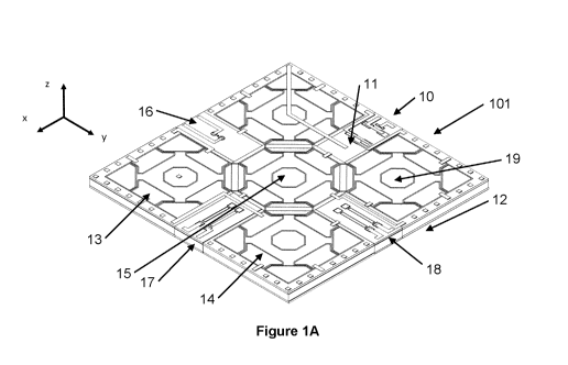
A single Micro-Electro-Mechanical System (MEMS) sensor chip is provided, for measuring multiple parameters, referred to as multiple degrees of freedom (DOF). The sensor chip comprises a central MEMS wafer bonded to a top cap wafer and a bottom cap wafer, all three wafer being electrically conductive. The sensor comprises at least two distinct sensors, each patterned in the electrically conductive MEMS wafer and in at least one of the top and bottom cap wafer. Insulated conducting pathways extend from electrical connections on the top or bottom cap wafers, through at least one of the electrically conductive top cap and bottom cap wafers, and through the electrically conductive MEMS wafer, to the sensors, for conducting electrical signals between the sensors and the electrical connections. The two or more distinct sensors are enclosed by the top and bottom cap wafers and by the outer frame of MEMS wafer.


French Abstract

L'invention concerne une puce de capteur de système micro-électro-mécanique (MEMS) unique, destinée à mesurer de multiples paramètres, désignés comme des multiples degrés de liberté (DOF). La puce de capteur comprend une plaquette de MEMS centrale liée à une plaquette de couverture supérieure et à une plaquette de couverture inférieure, les trois plaquettes étant électriquement conductrices. Le capteur comprend au moins deux capteurs distincts, chacun doté d'un motif dans la plaquette de MEMS électriquement conductrice et dans la plaquette de couverture supérieure et/ou la plaquette de couverture inférieure. Des chemins conducteurs isolés s'étendent depuis des raccords électriques sur les plaquettes de couverture supérieure ou inférieure, à travers la plaquette de couverture supérieure et/ou la plaquette de couverture inférieure électriquement conductrices et à travers la plaquette de MEMS électriquement conductrice, jusqu'aux capteurs, afin de conduire les signaux électriques entre les capteurs et les raccords électriques. Les deux capteurs distincts ou plus sont enserrés par les plaquettes de couverture supérieure et inférieure et par le cadre externe de la plaquette de MEMS.

Claims

Note: Claims are shown in the official language in which they were submitted.


41
CLAIMS
1. A single Micro-Electro-Mechanical System (MEMS) sensor chip for measuring
multiple parameters, referred to as multiple degrees of freedom (DOF), the
sensor
chip comprising:
an electrically conductive MEMS wafer having first and second sides and an
outer frame;
an electrically conductive top cap wafer having an inner top cap side and an
outer top cap side, the inner top cap side being bonded to the first side of
the
MEMS wafer;
an electrically conductive bottom cap wafer having an inner bottom cap side
and an outer bottom cap side, the inner bottom cap side being bonded to the
second side of the MEMS wafer,
at least one of the outer top cap side and the outer bottom cap side
comprising
electrical connections;
at least two distinct sensors, each patterned in the electrically conductive
MEMS wafer and in at least one of the top and bottom cap wafer, said sensors
being operative to sense at least two distinct parameters, respectively, along
at
least one of mutually orthogonal X, Y and Z axes; and
insulated conducting pathways extending from said electrical connections,
through at least one of the electrically conductive top cap and bottom cap
wafers,
and through the electrically conductive MEMS wafer, to said sensors, for
conducting electrical signals between said sensors and the electrical
connections,
said sensors being enclosed by the electrically conductive top and bottom cap
wafers and by the outer frame of the electrically conductive MEMS wafer.
2. The single MEMS sensor chip according to claim 1, wherein at least one of
said
sensors is hermetically sealed within said electrically conductive top and
bottom
cap wafers and by the electrically conducting MEMS wafer.

42
3. The single MEMS sensor chip according to claims 1 or 2, wherein one of said

sensors is a pressure sensor.
4. The single MEMS sensor chip according to any one of claims 1 to 3, wherein
one
of said sensors is 3-DOF magnetometer.
5. The single MEMS sensor chip according to any one of claims 1 to 4, wherein
one
of said sensors is an inertial sensor including at least one bulk proof mass
suspended in a cavity by flexible springs patterned in the electrically
conductive
MEMS wafer, the flexible springs enabling the bulk proof mass to move relative
to
the outer frame along the x, y and x axes, the cavity being defined by the
inner top
cap side and by the inner bottom cap side of the electrically conductive top
and
bottom cap wafers, and by sidewalls patterned in the electrically conductive
MEMS wafer.
6. The single MEMS sensor chip according to claim 5, wherein said inertial
sensor
comprises a 3-DOF accelerometer and one of said at least two distinct
parameters
is an acceleration of the MEMS sensor chip, wherein the at least one bulk
proof
mass comprises an accelerometer proof mass, the 3-DOF accelerometer
comprising accelerometer electrodes patterned in at least one of the
electrically
conductive top and bottom cap wafers, the accelerometer electrodes facing the
accelerometer proof mass and being operable to detect a translational motion
of
the accelerometer proof mass, indicative of the acceleration of the MEMS
sensor
chip along the X, Y and Z axes.
7. The single MEMS sensor chip according to claims 5 or 6, wherein said
inertial
sensor comprises a 3 DOF angular rate sensor and one of said at least two
distinct parameters is an angular rate of the MEMS sensor chip; wherein the at

least one bulk proof mass comprises at least one angular rate sensor proof
mass,

43
suspended in a corresponding angular rate cavity; the 3-DOF angular rate
sensor
comprising angular rate sensor electrodes patterned in at least one of the
electrically conductive top and bottom cap wafers, the angular rate sensor
electrodes facing the angular rate sensor proof mass and being operable to
drive
the angular rate proof mass and to detect a rocking motion of the angular rate

sensor proof mass, indicative of the angular rate of the MEMS sensor chip
about
the X, Y and Z axes.
8. The single MEMS sensor chip according to any one of claims 5 to 7, wherein
one
of said sensors is a pressure sensor and one of said parameters is a pressure,

said pressure sensor comprising :
a pressure sensor membrane patterned in the MEMS wafer and suspended
over at least one pressure sensor cavity, and
one or more pressure sensor electrode(s) patterned in at least one of the
electrically conductive top and bottom cap wafers and facing pressure sensor
membrane, the pressure sensor electrode(s) being operable to detect a
deflection
of said pressure sensor membrane, indicative of a variation of the pressure in
the
MEMS sensor chip.
9. The single MEMS sensor chip according to any one of claims 5 to 8, wherein
one
of said sensors is a 3-DOF magnetometer, and one of said parameters is a
magnetic field, the 3DOF magnetometer comprising:
two in-plane or X and Y magnetometers including :
resonant membranes, patterned in the MEMS wafer and aligned
with the X and Y axis respectively; and
magnetometer electrodes associated with the resonant
membranes and patterned in one of the electrically conductive top and
bottom cap wafers, the magnetometer electrodes being operatively
coupled to the resonant membranes, to detect motion of resonant

44
membranes along the Z axis, indicative of a component of a magnetic
field along the X or Y axis; and
one out-of-plane or Z magnetometer, including:
a comb structure patterned in the MEMS wafer, to detect a
motion of the comb sensor along one of the X or Y axis, indicative of a
component of a magnetic field along the Z axis,
whereby in use, alternating current is injected in the X, Y and Z
magnetometers, a Lorentz force acting on the resonant membranes
and/or comb structure in response to the magnetic field Image.
10. The single MEMS sensor chip according to any one of claims 1 to 9, wherein
the
electrically conductive MEMS, top cap and bottom cap wafers are made of an
electrically conductive silicon-based semiconductor material.
11. The single MEMS sensor chip according to any one of claims 1 to 9, wherein
the
electrically conductive MEMS wafer is a silicon-on-insulator (SOI) wafer, said
SOI
wafer including a device layer, a handle layer, and an insulating layer
sandwiched
between the device and handle layers.
12. The single MEMS sensor chip according to any one of claims 1 to 11,
wherein at
least one of the electrically conductive top cap and bottom cap wafers is an
SOI
wafer.
13. The single MEMS sensor chip according to claim 5 to 7, wherein the
pressure of
said cavity of the inertial sensor is under vacuum.
14.The single MEMS sensor chip according to claim 6, wherein the at least one
angular rate sensor proof mass comprises four different angular rate proof
masses, each suspended in corresponding angular rate sensor cavities.

45
15. The single MEMS sensor chip according to claim 8, wherein the at least one

pressure sensor cavity comprises first and second pressure sensor cavities,
the
first pressure sensor cavity being in fluid communication with an outside
atmosphere via a vent, and the second pressure sensor cavity being at a
predetermined pressure.
16. The single MEMS sensor chip according to claim 8 or 15, wherein the at
least one
pressure sensor cavity is circular, enabling a drum-like deflection of the
pressure
sensor membrane over its corresponding cavity.
17. The single MEMS sensor chip according to claim 9, wherein the resonant
membranes of the 3-DOF magnetometer includes longitudinal strips.
18. The single MEMS sensor chip according to claim 9 or 17, wherein the
electrically
conductive MEMS wafer is an SOI wafer comprising a handle layer and device
layer, the resonant membranes and the comb structure are patterned in the
device
layer of the electrically conductive MEMS wafer, the resonant membranes and
the
comb structure being suspended over magnetometer cavities etched in the handle

layers.
19. The single MEMS sensor chip according to claim 8, 15, or 16, wherein the
conductive MEMS wafer is an SOI wafer comprising a handle layer and device
layer, the pressure sensor membrane are patterned in the device layer of the
electrically conductive MEMS wafer, the pressure sensor membrane being
suspended over the pressure sensor cavity etched in the handle layer.
20. The single MEMS sensor chip according to any one of claims 1 to 19,
wherein at
least some of the insulated conducting pathways extend through the thickness
of
the electrically conductive top cap, MEMS or bottom cap wafers and have

46
sidewalls coated with an insulating material, said channel being filled with a

conducting material.
21. The single MEMS sensor chip according to any one of claims 1 to 4, wherein
each
of said at least two distinct sensors comprises electrodes patterned on the
inner
side of the electrically conductive top and bottom cap wafers and in the
electrically
conductive MEMS wafer, the electrodes being delineated by trenches filled with
an
insulating material.
22. The single MEMS sensor chip according to claim 21, wherein each of said
electrodes is connected to one of said electrical connections by way of a
corresponding one of the insulating conducting pathways.
23. The single MEMS sensor chip according to claim 1, said single MEMS sensor
chip
being a 10-DOF sensor chip wherein said at least two distinct sensors
comprises
a 3-DOF accelerometer, a 3-DOF angular rate sensor, a 1-DOF pressure sensor
and a 3-DOF magnetometer.
24. The single MEMS sensor chip according to claim 1, said single MEMS sensor
chip
being a 9-DOF sensor chip wherein said at least two distinct sensors comprises
a
3-DOF accelerometer, a 3-DOF angular rate sensor and a 3-DOF magnetometer.
25. The single MEMS sensor chip according to claim 1, said single MEMS sensor
chip
being a 7-DOF sensor chip wherein said at least two distinct sensors comprises
a
3-DOF accelerometer; a 3-DOF angular rate sensor, and a pressure sensor.

Description

Note: Descriptions are shown in the official language in which they were submitted.


CA 03013265 2018-07-31
WO 2016/145535 PCT/CA2016/050303
1
MULTIPLE DEGREE OF FREEDOM MEMS SENSOR CHIP AND METHOD FOR
FABRICATING THE SAME
TECHNICAL FIELD
The general technical field relates to Microelectromechanical Systems (MEMS)
Packaging, and more particularly to a method of fabricating a MEMS sensor with
a
hermetic package using Silicon-on-Insulator (S01) wafers.
BACKGROUND
Micro-electro-mechanical systems (MEMS) are an increasingly important enabling
technology. MEMS inertial sensors are used to sense changes in the state of
motion
of an object, including changes in position, velocity, acceleration or
orientation, and
encompass devices such as accelerometers, gyroscopes, vibrometers and
inclinometers. Broadly described, MEMS devices are integrated circuits (ICs)
containing tiny mechanical, optical, magnetic, electrical, chemical,
biological, or other,
transducers or actuators. MEMS devices can be manufactured using high-volume
silicon wafer fabrication techniques developed over the past fifty years for
the
microelectronics industry. Their resulting small size and low cost make them
attractive
for use in an increasing number of applications in a broad variety of
industries
including consumer, automotive, medical, aerospace, defense, green energy,
industrial, and other markets.
MEMS devices, in particular inertial sensors such as accelerometers and
angular rate
sensors or gyroscopes, are being used in a steadily growing number of
applications.
As the number of these applications grow, the greater the demand to add
additional
functionality and more types of MEMS into a system chip architecture. Due to
the
significant increase in consumer electronics applications for MEMS sensors
such as
optical image stabilization (01S) for cameras embedded in smart phones and
tablet
PCs, virtual reality systems and wearable electronics, there has been a
growing

Representative Drawing
A single figure which represents the drawing illustrating the invention.
Administrative Status

For a clearer understanding of the status of the application/patent presented on this page, the site Disclaimer , as well as the definitions for Patent , Administrative Status , Maintenance Fee  and Payment History  should be consulted.

Administrative Status

Title Date
Forecasted Issue Date Unavailable
(86) PCT Filing Date 2016-03-17
(87) PCT Publication Date 2016-09-22
(85) National Entry 2018-07-31
Examination Requested 2021-03-16

Abandonment History

Abandonment Date Reason Reinstatement Date
2019-03-18 FAILURE TO PAY APPLICATION MAINTENANCE FEE 2020-03-13

Maintenance Fee

Last Payment of $277.00 was received on 2024-03-07


 Upcoming maintenance fee amounts

Description Date Amount
Next Payment if small entity fee 2025-03-17 $100.00
Next Payment if standard fee 2025-03-17 $277.00

Note : If the full payment has not been received on or before the date indicated, a further fee may be required which may be one of the following

  • the reinstatement fee;
  • the late payment fee; or
  • additional fee to reverse deemed expiry.

Patent fees are adjusted on the 1st of January every year. The amounts above are the current amounts if received by December 31 of the current year.
Please refer to the CIPO Patent Fees web page to see all current fee amounts.

Payment History

Fee Type Anniversary Year Due Date Amount Paid Paid Date
Registration of a document - section 124 $100.00 2018-07-31
Reinstatement of rights $200.00 2018-07-31
Application Fee $400.00 2018-07-31
Maintenance Fee - Application - New Act 2 2018-03-19 $100.00 2018-07-31
Maintenance Fee - Application - New Act 3 2019-03-18 $100.00 2020-03-13
Reinstatement: Failure to Pay Application Maintenance Fees 2020-04-01 $200.00 2020-03-13
Maintenance Fee - Application - New Act 4 2020-04-01 $100.00 2020-03-13
Request for Examination 2021-03-17 $204.00 2021-03-16
Maintenance Fee - Application - New Act 5 2021-03-17 $204.00 2021-03-16
Maintenance Fee - Application - New Act 6 2022-03-17 $203.59 2022-03-07
Maintenance Fee - Application - New Act 7 2023-03-17 $210.51 2023-03-16
Continue Examination Fee - After NOA 2023-08-08 $816.00 2023-08-08
Continue Examination Fee - After NOA 2023-12-28 $816.00 2023-12-28
Maintenance Fee - Application - New Act 8 2024-03-18 $277.00 2024-03-07
Owners on Record

Note: Records showing the ownership history in alphabetical order.

Current Owners on Record
MOTION ENGINE INC.
Past Owners on Record
None
Past Owners that do not appear in the "Owners on Record" listing will appear in other documentation within the application.
Documents

To view selected files, please enter reCAPTCHA code :


To view images, click a link in the Document Description column. To download the documents, select one or more checkboxes in the first column and then click the "Download Selected in PDF format (Zip Archive)" or the "Download Selected as Single PDF" button.

List of published and non-published patent-specific documents on the CPD .

If you have any difficulty accessing content, you can call the Client Service Centre at 1-866-997-1936 or send them an e-mail at CIPO Client Service Centre.


Document
Description 
Date
(yyyy-mm-dd) 
Number of pages   Size of Image (KB) 
Reinstatement / Maintenance Fee Payment 2020-03-13 1 54
Maintenance Fee Payment 2020-03-13 1 47
Maintenance Fee Payment 2021-03-16 1 33
Request for Examination 2021-03-16 4 102
Description 2018-07-31 40 1,877
Examiner Requisition 2022-05-06 4 228
Amendment 2022-09-06 26 1,087
Description 2022-09-06 42 2,757
Claims 2022-09-06 8 481
Abstract 2018-07-31 1 83
Claims 2018-07-31 6 236
Drawings 2018-07-31 16 1,164
Representative Drawing 2018-07-31 1 46
International Search Report 2018-07-31 7 308
Declaration 2018-07-31 1 42
National Entry Request 2018-07-31 10 279
Cover Page 2018-08-09 1 3
Notice of Allowance response includes a RCE / Amendment 2023-12-28 6 177
Maintenance Fee Payment 2024-03-07 1 33
Amendment 2024-03-18 96 4,096
Description 2024-03-18 54 3,616
Claims 2024-03-18 33 1,946
Examiner Requisition 2024-04-04 4 201
Notice of Allowance response includes a RCE / Amendment 2023-08-08 41 1,706
Description 2023-08-08 44 2,864
Claims 2023-08-08 21 1,246
Prosecution Correspondence 2023-10-05 5 143
Office Letter 2023-10-16 1 183