Sélection de la langue

Search

Sommaire du brevet 3013265 

Énoncé de désistement de responsabilité concernant l'information provenant de tiers

Une partie des informations de ce site Web a été fournie par des sources externes. Le gouvernement du Canada n'assume aucune responsabilité concernant la précision, l'actualité ou la fiabilité des informations fournies par les sources externes. Les utilisateurs qui désirent employer cette information devraient consulter directement la source des informations. Le contenu fourni par les sources externes n'est pas assujetti aux exigences sur les langues officielles, la protection des renseignements personnels et l'accessibilité.

Disponibilité de l'Abrégé et des Revendications

L'apparition de différences dans le texte et l'image des Revendications et de l'Abrégé dépend du moment auquel le document est publié. Les textes des Revendications et de l'Abrégé sont affichés :

  • lorsque la demande peut être examinée par le public;
  • lorsque le brevet est émis (délivrance).
(12) Demande de brevet: (11) CA 3013265
(54) Titre français: PUCE DE CAPTEUR MEMS A MULTIPLES DEGRES DE LIBERTE ET SON PROCEDE DE FABRICATION
(54) Titre anglais: MULTIPLE DEGREE OF FREEDOM MEMS SENSOR CHIP AND METHOD FOR FABRICATING THE SAME
Statut: Rapport envoyé
Données bibliographiques
(51) Classification internationale des brevets (CIB):
  • B81B 7/02 (2006.01)
  • G01C 19/574 (2012.01)
  • G01D 21/02 (2006.01)
  • G01L 9/00 (2006.01)
  • G01P 15/08 (2006.01)
  • G01P 15/18 (2013.01)
  • G01R 33/028 (2006.01)
(72) Inventeurs :
  • BOYSEL, ROBERT MARK (Canada)
(73) Titulaires :
  • MOTION ENGINE INC. (Canada)
(71) Demandeurs :
  • MOTION ENGINE INC. (Canada)
(74) Agent: ROBIC AGENCE PI S.E.C./ROBIC IP AGENCY LP
(74) Co-agent:
(45) Délivré:
(86) Date de dépôt PCT: 2016-03-17
(87) Mise à la disponibilité du public: 2016-09-22
Requête d'examen: 2021-03-16
Licence disponible: S.O.
(25) Langue des documents déposés: Anglais

Traité de coopération en matière de brevets (PCT): Oui
(86) Numéro de la demande PCT: PCT/CA2016/050303
(87) Numéro de publication internationale PCT: WO2016/145535
(85) Entrée nationale: 2018-07-31

(30) Données de priorité de la demande:
Numéro de la demande Pays / territoire Date
62/134,832 Etats-Unis d'Amérique 2015-03-18

Abrégés

Abrégé français

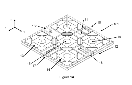
L'invention concerne une puce de capteur de système micro-électro-mécanique (MEMS) unique, destinée à mesurer de multiples paramètres, désignés comme des multiples degrés de liberté (DOF). La puce de capteur comprend une plaquette de MEMS centrale liée à une plaquette de couverture supérieure et à une plaquette de couverture inférieure, les trois plaquettes étant électriquement conductrices. Le capteur comprend au moins deux capteurs distincts, chacun doté d'un motif dans la plaquette de MEMS électriquement conductrice et dans la plaquette de couverture supérieure et/ou la plaquette de couverture inférieure. Des chemins conducteurs isolés s'étendent depuis des raccords électriques sur les plaquettes de couverture supérieure ou inférieure, à travers la plaquette de couverture supérieure et/ou la plaquette de couverture inférieure électriquement conductrices et à travers la plaquette de MEMS électriquement conductrice, jusqu'aux capteurs, afin de conduire les signaux électriques entre les capteurs et les raccords électriques. Les deux capteurs distincts ou plus sont enserrés par les plaquettes de couverture supérieure et inférieure et par le cadre externe de la plaquette de MEMS.


Abrégé anglais

A single Micro-Electro-Mechanical System (MEMS) sensor chip is provided, for measuring multiple parameters, referred to as multiple degrees of freedom (DOF). The sensor chip comprises a central MEMS wafer bonded to a top cap wafer and a bottom cap wafer, all three wafer being electrically conductive. The sensor comprises at least two distinct sensors, each patterned in the electrically conductive MEMS wafer and in at least one of the top and bottom cap wafer. Insulated conducting pathways extend from electrical connections on the top or bottom cap wafers, through at least one of the electrically conductive top cap and bottom cap wafers, and through the electrically conductive MEMS wafer, to the sensors, for conducting electrical signals between the sensors and the electrical connections. The two or more distinct sensors are enclosed by the top and bottom cap wafers and by the outer frame of MEMS wafer.

Revendications

Note : Les revendications sont présentées dans la langue officielle dans laquelle elles ont été soumises.


41
CLAIMS
1. A single Micro-Electro-Mechanical System (MEMS) sensor chip for measuring
multiple parameters, referred to as multiple degrees of freedom (DOF), the
sensor
chip comprising:
an electrically conductive MEMS wafer having first and second sides and an
outer frame;
an electrically conductive top cap wafer having an inner top cap side and an
outer top cap side, the inner top cap side being bonded to the first side of
the
MEMS wafer;
an electrically conductive bottom cap wafer having an inner bottom cap side
and an outer bottom cap side, the inner bottom cap side being bonded to the
second side of the MEMS wafer,
at least one of the outer top cap side and the outer bottom cap side
comprising
electrical connections;
at least two distinct sensors, each patterned in the electrically conductive
MEMS wafer and in at least one of the top and bottom cap wafer, said sensors
being operative to sense at least two distinct parameters, respectively, along
at
least one of mutually orthogonal X, Y and Z axes; and
insulated conducting pathways extending from said electrical connections,
through at least one of the electrically conductive top cap and bottom cap
wafers,
and through the electrically conductive MEMS wafer, to said sensors, for
conducting electrical signals between said sensors and the electrical
connections,
said sensors being enclosed by the electrically conductive top and bottom cap
wafers and by the outer frame of the electrically conductive MEMS wafer.
2. The single MEMS sensor chip according to claim 1, wherein at least one of
said
sensors is hermetically sealed within said electrically conductive top and
bottom
cap wafers and by the electrically conducting MEMS wafer.

42
3. The single MEMS sensor chip according to claims 1 or 2, wherein one of said

sensors is a pressure sensor.
4. The single MEMS sensor chip according to any one of claims 1 to 3, wherein
one
of said sensors is 3-DOF magnetometer.
5. The single MEMS sensor chip according to any one of claims 1 to 4, wherein
one
of said sensors is an inertial sensor including at least one bulk proof mass
suspended in a cavity by flexible springs patterned in the electrically
conductive
MEMS wafer, the flexible springs enabling the bulk proof mass to move relative
to
the outer frame along the x, y and x axes, the cavity being defined by the
inner top
cap side and by the inner bottom cap side of the electrically conductive top
and
bottom cap wafers, and by sidewalls patterned in the electrically conductive
MEMS wafer.
6. The single MEMS sensor chip according to claim 5, wherein said inertial
sensor
comprises a 3-DOF accelerometer and one of said at least two distinct
parameters
is an acceleration of the MEMS sensor chip, wherein the at least one bulk
proof
mass comprises an accelerometer proof mass, the 3-DOF accelerometer
comprising accelerometer electrodes patterned in at least one of the
electrically
conductive top and bottom cap wafers, the accelerometer electrodes facing the
accelerometer proof mass and being operable to detect a translational motion
of
the accelerometer proof mass, indicative of the acceleration of the MEMS
sensor
chip along the X, Y and Z axes.
7. The single MEMS sensor chip according to claims 5 or 6, wherein said
inertial
sensor comprises a 3 DOF angular rate sensor and one of said at least two
distinct parameters is an angular rate of the MEMS sensor chip; wherein the at

least one bulk proof mass comprises at least one angular rate sensor proof
mass,

43
suspended in a corresponding angular rate cavity; the 3-DOF angular rate
sensor
comprising angular rate sensor electrodes patterned in at least one of the
electrically conductive top and bottom cap wafers, the angular rate sensor
electrodes facing the angular rate sensor proof mass and being operable to
drive
the angular rate proof mass and to detect a rocking motion of the angular rate

sensor proof mass, indicative of the angular rate of the MEMS sensor chip
about
the X, Y and Z axes.
8. The single MEMS sensor chip according to any one of claims 5 to 7, wherein
one
of said sensors is a pressure sensor and one of said parameters is a pressure,

said pressure sensor comprising :
a pressure sensor membrane patterned in the MEMS wafer and suspended
over at least one pressure sensor cavity, and
one or more pressure sensor electrode(s) patterned in at least one of the
electrically conductive top and bottom cap wafers and facing pressure sensor
membrane, the pressure sensor electrode(s) being operable to detect a
deflection
of said pressure sensor membrane, indicative of a variation of the pressure in
the
MEMS sensor chip.
9. The single MEMS sensor chip according to any one of claims 5 to 8, wherein
one
of said sensors is a 3-DOF magnetometer, and one of said parameters is a
magnetic field, the 3DOF magnetometer comprising:
two in-plane or X and Y magnetometers including :
resonant membranes, patterned in the MEMS wafer and aligned
with the X and Y axis respectively; and
magnetometer electrodes associated with the resonant
membranes and patterned in one of the electrically conductive top and
bottom cap wafers, the magnetometer electrodes being operatively
coupled to the resonant membranes, to detect motion of resonant

44
membranes along the Z axis, indicative of a component of a magnetic
field along the X or Y axis; and
one out-of-plane or Z magnetometer, including:
a comb structure patterned in the MEMS wafer, to detect a
motion of the comb sensor along one of the X or Y axis, indicative of a
component of a magnetic field along the Z axis,
whereby in use, alternating current is injected in the X, Y and Z
magnetometers, a Lorentz force acting on the resonant membranes
and/or comb structure in response to the magnetic field Image.
10. The single MEMS sensor chip according to any one of claims 1 to 9, wherein
the
electrically conductive MEMS, top cap and bottom cap wafers are made of an
electrically conductive silicon-based semiconductor material.
11. The single MEMS sensor chip according to any one of claims 1 to 9, wherein
the
electrically conductive MEMS wafer is a silicon-on-insulator (SOI) wafer, said
SOI
wafer including a device layer, a handle layer, and an insulating layer
sandwiched
between the device and handle layers.
12. The single MEMS sensor chip according to any one of claims 1 to 11,
wherein at
least one of the electrically conductive top cap and bottom cap wafers is an
SOI
wafer.
13. The single MEMS sensor chip according to claim 5 to 7, wherein the
pressure of
said cavity of the inertial sensor is under vacuum.
14.The single MEMS sensor chip according to claim 6, wherein the at least one
angular rate sensor proof mass comprises four different angular rate proof
masses, each suspended in corresponding angular rate sensor cavities.

45
15. The single MEMS sensor chip according to claim 8, wherein the at least one

pressure sensor cavity comprises first and second pressure sensor cavities,
the
first pressure sensor cavity being in fluid communication with an outside
atmosphere via a vent, and the second pressure sensor cavity being at a
predetermined pressure.
16. The single MEMS sensor chip according to claim 8 or 15, wherein the at
least one
pressure sensor cavity is circular, enabling a drum-like deflection of the
pressure
sensor membrane over its corresponding cavity.
17. The single MEMS sensor chip according to claim 9, wherein the resonant
membranes of the 3-DOF magnetometer includes longitudinal strips.
18. The single MEMS sensor chip according to claim 9 or 17, wherein the
electrically
conductive MEMS wafer is an SOI wafer comprising a handle layer and device
layer, the resonant membranes and the comb structure are patterned in the
device
layer of the electrically conductive MEMS wafer, the resonant membranes and
the
comb structure being suspended over magnetometer cavities etched in the handle

layers.
19. The single MEMS sensor chip according to claim 8, 15, or 16, wherein the
conductive MEMS wafer is an SOI wafer comprising a handle layer and device
layer, the pressure sensor membrane are patterned in the device layer of the
electrically conductive MEMS wafer, the pressure sensor membrane being
suspended over the pressure sensor cavity etched in the handle layer.
20. The single MEMS sensor chip according to any one of claims 1 to 19,
wherein at
least some of the insulated conducting pathways extend through the thickness
of
the electrically conductive top cap, MEMS or bottom cap wafers and have

46
sidewalls coated with an insulating material, said channel being filled with a

conducting material.
21. The single MEMS sensor chip according to any one of claims 1 to 4, wherein
each
of said at least two distinct sensors comprises electrodes patterned on the
inner
side of the electrically conductive top and bottom cap wafers and in the
electrically
conductive MEMS wafer, the electrodes being delineated by trenches filled with
an
insulating material.
22. The single MEMS sensor chip according to claim 21, wherein each of said
electrodes is connected to one of said electrical connections by way of a
corresponding one of the insulating conducting pathways.
23. The single MEMS sensor chip according to claim 1, said single MEMS sensor
chip
being a 10-DOF sensor chip wherein said at least two distinct sensors
comprises
a 3-DOF accelerometer, a 3-DOF angular rate sensor, a 1-DOF pressure sensor
and a 3-DOF magnetometer.
24. The single MEMS sensor chip according to claim 1, said single MEMS sensor
chip
being a 9-DOF sensor chip wherein said at least two distinct sensors comprises
a
3-DOF accelerometer, a 3-DOF angular rate sensor and a 3-DOF magnetometer.
25. The single MEMS sensor chip according to claim 1, said single MEMS sensor
chip
being a 7-DOF sensor chip wherein said at least two distinct sensors comprises
a
3-DOF accelerometer; a 3-DOF angular rate sensor, and a pressure sensor.

Description

Note : Les descriptions sont présentées dans la langue officielle dans laquelle elles ont été soumises.


CA 03013265 2018-07-31
WO 2016/145535 PCT/CA2016/050303
1
MULTIPLE DEGREE OF FREEDOM MEMS SENSOR CHIP AND METHOD FOR
FABRICATING THE SAME
TECHNICAL FIELD
The general technical field relates to Microelectromechanical Systems (MEMS)
Packaging, and more particularly to a method of fabricating a MEMS sensor with
a
hermetic package using Silicon-on-Insulator (S01) wafers.
BACKGROUND
Micro-electro-mechanical systems (MEMS) are an increasingly important enabling
technology. MEMS inertial sensors are used to sense changes in the state of
motion
of an object, including changes in position, velocity, acceleration or
orientation, and
encompass devices such as accelerometers, gyroscopes, vibrometers and
inclinometers. Broadly described, MEMS devices are integrated circuits (ICs)
containing tiny mechanical, optical, magnetic, electrical, chemical,
biological, or other,
transducers or actuators. MEMS devices can be manufactured using high-volume
silicon wafer fabrication techniques developed over the past fifty years for
the
microelectronics industry. Their resulting small size and low cost make them
attractive
for use in an increasing number of applications in a broad variety of
industries
including consumer, automotive, medical, aerospace, defense, green energy,
industrial, and other markets.
MEMS devices, in particular inertial sensors such as accelerometers and
angular rate
sensors or gyroscopes, are being used in a steadily growing number of
applications.
As the number of these applications grow, the greater the demand to add
additional
functionality and more types of MEMS into a system chip architecture. Due to
the
significant increase in consumer electronics applications for MEMS sensors
such as
optical image stabilization (01S) for cameras embedded in smart phones and
tablet
PCs, virtual reality systems and wearable electronics, there has been a
growing

Dessin représentatif
Une figure unique qui représente un dessin illustrant l'invention.
États administratifs

Pour une meilleure compréhension de l'état de la demande ou brevet qui figure sur cette page, la rubrique Mise en garde , et les descriptions de Brevet , États administratifs , Taxes périodiques et Historique des paiements devraient être consultées.

États administratifs

Titre Date
Date de délivrance prévu Non disponible
(86) Date de dépôt PCT 2016-03-17
(87) Date de publication PCT 2016-09-22
(85) Entrée nationale 2018-07-31
Requête d'examen 2021-03-16

Historique d'abandonnement

Date d'abandonnement Raison Reinstatement Date
2019-03-18 Taxe périodique sur la demande impayée 2020-03-13

Taxes périodiques

Dernier paiement au montant de 277,00 $ a été reçu le 2024-03-07


 Montants des taxes pour le maintien en état à venir

Description Date Montant
Prochain paiement si taxe applicable aux petites entités 2025-03-17 100,00 $
Prochain paiement si taxe générale 2025-03-17 277,00 $

Avis : Si le paiement en totalité n'a pas été reçu au plus tard à la date indiquée, une taxe supplémentaire peut être imposée, soit une des taxes suivantes :

  • taxe de rétablissement ;
  • taxe pour paiement en souffrance ; ou
  • taxe additionnelle pour le renversement d'une péremption réputée.

Les taxes sur les brevets sont ajustées au 1er janvier de chaque année. Les montants ci-dessus sont les montants actuels s'ils sont reçus au plus tard le 31 décembre de l'année en cours.
Veuillez vous référer à la page web des taxes sur les brevets de l'OPIC pour voir tous les montants actuels des taxes.

Historique des paiements

Type de taxes Anniversaire Échéance Montant payé Date payée
Enregistrement de documents 100,00 $ 2018-07-31
Rétablissement des droits 200,00 $ 2018-07-31
Le dépôt d'une demande de brevet 400,00 $ 2018-07-31
Taxe de maintien en état - Demande - nouvelle loi 2 2018-03-19 100,00 $ 2018-07-31
Taxe de maintien en état - Demande - nouvelle loi 3 2019-03-18 100,00 $ 2020-03-13
Rétablissement: taxe de maintien en état non-payées pour la demande 2020-04-01 200,00 $ 2020-03-13
Taxe de maintien en état - Demande - nouvelle loi 4 2020-04-01 100,00 $ 2020-03-13
Requête d'examen 2021-03-17 204,00 $ 2021-03-16
Taxe de maintien en état - Demande - nouvelle loi 5 2021-03-17 204,00 $ 2021-03-16
Taxe de maintien en état - Demande - nouvelle loi 6 2022-03-17 203,59 $ 2022-03-07
Taxe de maintien en état - Demande - nouvelle loi 7 2023-03-17 210,51 $ 2023-03-16
Taxe pour la poursuite de l'examen - après l'AA 2023-08-08 816,00 $ 2023-08-08
Taxe pour la poursuite de l'examen - après l'AA 2023-12-28 816,00 $ 2023-12-28
Taxe de maintien en état - Demande - nouvelle loi 8 2024-03-18 277,00 $ 2024-03-07
Titulaires au dossier

Les titulaires actuels et antérieures au dossier sont affichés en ordre alphabétique.

Titulaires actuels au dossier
MOTION ENGINE INC.
Titulaires antérieures au dossier
S.O.
Les propriétaires antérieurs qui ne figurent pas dans la liste des « Propriétaires au dossier » apparaîtront dans d'autres documents au dossier.
Documents

Pour visionner les fichiers sélectionnés, entrer le code reCAPTCHA :


Pour visualiser une image, cliquer sur un lien dans la colonne description du document. Pour télécharger l'image (les images), cliquer l'une ou plusieurs cases à cocher dans la première colonne et ensuite cliquer sur le bouton "Télécharger sélection en format PDF (archive Zip)" ou le bouton "Télécharger sélection (en un fichier PDF fusionné)".

Liste des documents de brevet publiés et non publiés sur la BDBC .

Si vous avez des difficultés à accéder au contenu, veuillez communiquer avec le Centre de services à la clientèle au 1-866-997-1936, ou envoyer un courriel au Centre de service à la clientèle de l'OPIC.


Description du
Document 
Date
(yyyy-mm-dd) 
Nombre de pages   Taille de l'image (Ko) 
Rétablissement / Paiement de taxe périodique 2020-03-13 1 54
Paiement de taxe périodique 2020-03-13 1 47
Paiement de taxe périodique 2021-03-16 1 33
Requête d'examen 2021-03-16 4 102
Description 2018-07-31 40 1 877
Demande d'examen 2022-05-06 4 228
Modification 2022-09-06 26 1 087
Description 2022-09-06 42 2 757
Revendications 2022-09-06 8 481
Abrégé 2018-07-31 1 83
Revendications 2018-07-31 6 236
Dessins 2018-07-31 16 1 164
Dessins représentatifs 2018-07-31 1 46
Rapport de recherche internationale 2018-07-31 7 308
Déclaration 2018-07-31 1 42
Demande d'entrée en phase nationale 2018-07-31 10 279
Page couverture 2018-08-09 1 3
Réponse à l'avis d'acceptation inclut la RPE / Modification 2023-12-28 6 177
Paiement de taxe périodique 2024-03-07 1 33
Modification 2024-03-18 96 4 096
Description 2024-03-18 54 3 616
Revendications 2024-03-18 33 1 946
Demande d'examen 2024-04-04 4 201
Réponse à l'avis d'acceptation inclut la RPE / Modification 2023-08-08 41 1 706
Description 2023-08-08 44 2 864
Revendications 2023-08-08 21 1 246
Correspondance de la poursuite 2023-10-05 5 143
Lettre du bureau 2023-10-16 1 183