Note : Les descriptions sont présentées dans la langue officielle dans laquelle elles ont été soumises.
lZ6Z~7~
27780-1
B KGROUND OF' T~IE INVENTION_
1. Technical Field
The present inven-ti.on relates to the field oE clock
systems or digital telecommunications systems and particularly to
a clock regenerator whose phase is corrected through a phase
locked loop.
2. Description of the Prior Art
In digital communications technology there are o~ten
used, besides passive clock regenerators or clock extractors,
active clock regenerators which opera-te with an additional
oscillator signal.
SUMMARY OF THE INV~NTION
By the present invention, a specific solution for an
active clock regenerator is indicated which operates relatively
quickly and has an especially good jitter tolerance.
According to a broad aspect of the invention, there is
provided a clock regenerator comprising a programmable divisor
circuit which is connected to -the output of an oscillator and
having as an output a regenerated signal; a comparator circuit
having a received input eye signal for transforming said input eye
signal into input pulses; a phase detector Eor comparing the
regenerated signal with the input pulses by means of an oscill.ator
signal from said oscillator and which provides a lead signal and a
l.ag signal, said phase detector being configured as a phase locked
loop having an oscillator frequency of approximately N times
higher than the regenerated requency; and a loop filter control-
- 2 -
2~l~7':-~
27780~1
led by the lead and lag signals, wherein the loop f;.lter comprises
a first logic circuit which delivers an information siynal, a
reset signal and control signals; a second logi.c circuit which
receives the lead and lag signals and the information signal to
indicate the sign and, the direction of the counting status and
which provides a counter clock signal and a count direction si.gnal
for a counter having a reset input for receiving the signal, and
wherein said first logic circuit has an input connected to the
output of the counter, and wherein the regenerated signal has at
least one delayed signal delayed by L/~ periods where L is a low
integer, to derive from the delayed signal a pulse window having
at least three zones; and output signals of the phase detector
represent which zone includes the edge of the input signal; and
first logic circuit for controlling the programmable divisor such
that, when the edges of the input pulses fall in the most central
zone of the three zones, the counter counts toward zero and no
correction of the output signal is initiated, and wherein the
status of said counter is stored in said first logic circuit.
In -the following, the invention will be explained more
specifically by a description of embodiments with reference to
drawings.
- 2a -
..~,
~ .
BPIEF DESC~IPTION C~F ~IE DRawI~lGs
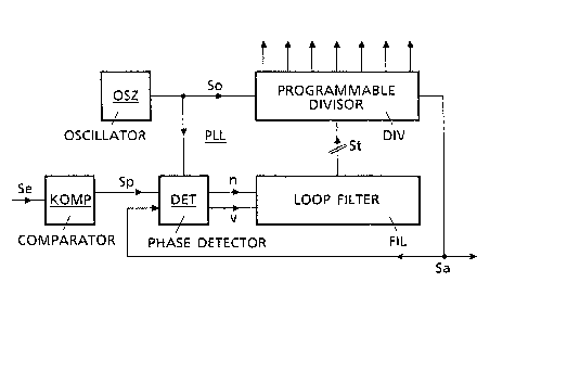
Fig. 1 shows the circuit diagram o~ a clock regenerator
according to the invention;
Flg. 2 shows the circuit diagram of a loop Filter for such a
clock regenerator;
Fig. 3 shows a timing diaaram for various signals; and
Fig. 4 shows the circuit diagram of a phase detector for such a
clock regenerator.
DETAILED DESCRIPTIûN
The clock regenerator according to Fig. 1 comprises a
programmable divisor DIV, which is connected to the output o~ an
oscillator OSZ, and whose output signal Sa has a frequency fa which
is smaller than the ~requency fo of the oscillator signal So by
approximately the factor N. The clock reaenerator further comprises
a comparator circuit KOMP, where a received eye signal Se transforms
into pulses Sp, as well as a phase detector DET and a loop filter
FIL whose output signal St controls the divisor DIV. The phase
detector DET compares the signals Sp and Sa by means of the signal
~5~ So and delivers two signals n and v, with which the loop filter is
controlled.
The clock regenerator according to FigO 1 is constructed in
principle like a phase locked loop (PLL) circuit, so that the
principle of its operation is known.
The loop filter accordinn to Fig. 2 comprises a counter C and
two logic circuits LOGl and LCG2, of which the second receives the
~21~
signals n and v, and the first delivers the control signal St as
well as an information signal m ~or the control of circuit LOG2 and
a reset sianal r for counter C. On the input side, circuit LO~l is
connected to the various outputs of counter C, the clock input El of
which receives a first output signal 9 while its count direction
input E2 receives a second output signal h of circuit LOG2.
The clock regenerator accordina to Fig. l and 2 operates as
follows:
The programmable divisor DIv normally divides the output
frequency fo of oscillator OSZ (Fig. 1~ by N, to obtain a clock
signal Sa which has approximately the same frequency fa as the
frequency fe of arriving sianal Se. The phase detector DET compares
the phase of the synthesized pulses Sa with those of the pulses Sp
obtained at the output of the comparator circuit KûMP and tests how
much the edges of signal Sa arrive before or after the edges of
signal Sp.
For this purpose the clock signal Sa undergoes in the phase
detector DET a delay of any desired duration, which may also be
zero. The resulting clock signal Sal (Fig. 3) is then further
delayed in such a way that there results a clock signal Sa2 delayed
by L/N periods relative to clock si~nal Sal, where L is a small
integer, preferably L = l. Thus there results the pulse window
shown in
Fig. 3, with four zones I, II, III an~ IV, as follows:
Zone I Sal = û and Sa2 = O
Zone II Sal = l and Sa2 = O
Zone III Sal = l and Sa2 = l
Zone IV Sal = O and Sa2 = l
-- 4 --
7~
Every time an ascending edge o~` the signal Sp arrives, whic~ may
be jittered, pulses n and v are generated, namely, depending on the
zone I, II, III or IV in which the edge is located, accordin~ to the
following Ru~e I:
Zone I n = l and v = O
Zone II n = l and v = l
Zone III n = O and v - l
Zone IV n = O and v = O
Here, n = O or v = O means that at the moment there is no pulse,
and n = l or v = l means that at the moment there is a pulse, for
example, a half bit wide. From the pulses n, v and m are ~enerated
by the circuit LOG2 the clock pulse ~ as well as the signal h
serving to control the counting direction. The counter status of
counter C is recognized by the circuit lOGl, so that for a positive
counting status, for example, the signal m has the value m = l.
The counter C starts to count at a value O and counts according
to the following Rule II:
With every pulse v = l, the counter C counts in a positive
direction by a value X, for example, from ~6 to +7 or from -3 to -2,
with X = l. With every pulse n = l, the counter counts in negative
direction by a value X, for example from -6 to -7 or from ~3 to +2,
with X = l. When simultaneously v = l and n = l, the counter counts
by a value Y toward zero, for example from ~6 to +5 with Y = l at m
-l or from -6 to -5 at m = O. If no edge arrives, v = O and n = O
simultaneously, and the counter does not count.
As long as the counter status has not reached a value ~K or -K,
the control si~nal St receives the information that the divisor DIV
(rig. 1) is tc divide by N. When the counter status reaches the
.~ i2~'7~
value +K, the control signal St brin~s it about that the divisor DIV
divides by (N -~ l) instead of by N, as a result of which the
~rquency ~a of clock signal Sa becomes smaller; but when the counter
status reaches the value -K, the control s:ignal St brings it ahout
that the divisor DIV divides by (N - l) instead of by N, as a result
of which the frequency fa of clock signal Sa becomes greater. In
the last two cases, however, a change of the signal r is caused at
the same time, by which the counter C (Fig. 2) is set to zero.
The clock regenerator according to the invention brings about a
rapid correction of the phase difference if the clock signals Sa and
Sp are not in phase9 and at the same time it prevents unnecessary
and disturbing corrections when the clock signals Sa and Sp are in
phase. Furthermore the clock regenerator functions satisfactorily
also when clock signal Sp is jittered.
If all jittered pulse edges fall in zone II, that is, if n = l
and v = l, the counter C counts toward zero, and no correction is
brought about. If there are more pulses in zone III (with n = 0 and
v = l) than in zone II (with n = l and v = l), the counter status
approaches the threshold +K faster, the grater the proportion of
pulses lying in zone III is. If there are more pulses in zone I
(with n = l and v = 0) than in zone II, the counter status
approaches the threshold -K faster, the greater the proportion of
pulses lying in zone I is. If there are pulses only in zone III,
the counter status immediately rises to the threshold +K; if there
are pulses only in zone I, it counts immediately up to the threshold
-K~
The phase detector shown in Fig. 4 comprises two multivibrators
FFl and FF2 which are responsible for the delay of pulse signal Sa2,
as ~/ell as four additional multivibrators FF3, FF4, FF5 and FF6, a
NAN0 gate ~ and t~o AND gates Ul and U2, which serve to realize Rule
..1.i~tj2:1 7'1~ `
I. In Fig. 3 are shown the pulses n and v, which result in the case
that the edge of signal Sp falls in zone I, II, or III. For zone IV
there applies ~or a detector accordinq to Fig. 1, n= O and v _ C.
As 7one IV is irrelevant, other detectors may be used where n , O,
v = 1 or n - 1, v = O.
Lastly let it be noted that with every correction the clock
signal Sa is readjusted in phase, for example, by l/rl period, but it
will then run away again faster the greater the deviation is between
the frequencies fe and fo/N. Hence clock signal Sa is subject to a
systematic jitter of the magnitude 1/N period. However, the method
according to the invention proves advantageous because without the
two clock signals Sal and Sa2, a systematic jitter of the maonitude
~ instead of l/N period would result.
~ 6
As a variant of the invention, the counter C may be such that it
counts in larger steps than X = 1 if the counter status is closer to
one of the thresholds +K or -K respectively. For this purpose there
may be provided, for example, five, seven or more zones. ~esides,
the divisor DIV can be designed to deliver a plurality of signals of
a frequency fa, 2fa, 4fa, ... and/or (i/j) fa, e.g. (6/5) fa. Other
embodiments and variations of embodiments should be deemed within
the scope of those ordinarilly skilled in the art and the invention
should only be considered limited by the scope of the claims which
~5 follow.