Note : Les descriptions sont présentées dans la langue officielle dans laquelle elles ont été soumises.
:~26~
IMPROVED MODEM CONTROLLER
This application is a division of Canadian
Serial No. 521,043, filed October 21, 1986.
3~b~ ~ r
The pre~ent inventi on relate~ to tha3!
control and operation of mode~a~ and particularly
di~clo~es an improved modem con~roller which allc~
all configuration parameter~ 'co be qelected by using
an a~ynchronou~ data terminAl r~ther than ~witches,
and provides ~3witching and ~toring of operating
parameters in re~ponse to variou~ input~, including
f luctuation~ in power ~upply input voltage .
B~ekqround of ~he Inv~tlos~ ,
2$ The rapid growth in the use of digital
co~puting machines creat-ed a need for a data
communicatioll~ device which would enable digital
computing machine~ to communicate with each other
over standard voice-grade telephone line~. The
answer to thi~ need came in the form of a data
modulator-demodulator device~ commonly called a
mode~n.
Modem~ are fr~quen~ly required to be able
to acco~odate a variety of modulation ~chemes, b~t
rate~ " and d~ta ormats, antl to operate in either
half-duplex or full-duplex mode. Alqo, m~ny modern
intelligent modem~ provide automatlc answer ing of
incoming call~, and both dual tone multiple frequency
( "tone dialing" ) and rotary pulse dl2lling of
S user-selected telephone numbers. The~e modulation
scheme~, bit rate~, data format~" and other feature~
are oten referred to a~ operating parameter~. A
particular combina~ion of operating para~eter~ may be
convenien~ly referred to ~ a configur~t~on pro:ElleO
A typical modem will ha~e al read orlly
memory (RO~) with a factory ~etting of so~e of the
operating parameters, commonly c~lled def ault
~ettings, but not a complete conf lguration prof ile .
A ROM i~ programmed by the manuf2lcturer and
15 "remember~" the default ~etting~ even when power is
turned off for an extended 'cislle. ~he remainder oiE
the operating parameter~ are ~et by using internal
and external ~witches. The internnl ~witche~ are
u~ually not easily acce~sible. The typlcal modem
will al~o allow the u~er, by u~ing hi~ data terminal,
to override the default ~ettings and command the
modem to u~e anvther par.tial set of operating
parameter~, commonly called active parameter~, which
are ~tored in a volatile memory. A volatile memory
25 will "forget~ it~ content~ if the power i~ turned of f .
Therefore, some modems have a battery which provide~
power to the memory for a short time in the event
that 'che main power i~ turned off. The remainder of
the operating parameters are again ~et by the same
30 internal and external ~witche~.
Neither the P~OM nor the volati le me~nory
stores a complete configura'cion profile. The
operating parameters norm~lly set by internal
~witche~ are one~ which are unlikely to change often
35 ana/or are determined by the other equipment with
1~6~
which the modem i~ u~ed. Some of the operating
parameter~ which are typically set by internal
~witche~ are: whether the mode~ r2sponds to the data
terminal ready ~ignal; whether the modem send3 re~ult
S and error code~ as English word~ number~, or not ~t
all; whether or slot the modem echoe~ the data back to
the data t~rminal O whether or not the modem will
an~wer all incomirlg call; whether or not the llnodem
will advise the dat~ terminal if the carrler i8
pre~en~ on the ~3lephone l~ne whg~t type of ~lephone
cireuit the modem 1~ connected to; and whether th~
~nodem i~ in an intelligeslt or dumb de.
Some o the op~rating parame~er~ which ar~
typically Yet by axternal 3wltches ar~: ~anu~l re~et
lS of the modem; high ~peed or low ~peed com~unicat~on~
self -test of the modem-to ~elephone line interf ace
circuits; te~ting of the devlce connected to the
other end of Jche telephone lin~9
Some of the op~rating parameter3 which are
typically ~tored in the read only memory a~ factory
default ~etting~ are- a modem operating speed of
0-300, 600, 1200 or 2400 bit3 per ~es:ond; 7 or a bits
per chalracter; odd" even, or no parity; number of
~top bit~ per character; selection of automatic
an~wer; the number of ring3 before the modem will
pick up the telephone line; tone or pulse dialing;
~hether or not a line feed ~ignal i~ sent af ter a
carriage return ~ignal; hvw long the modem wait~ for
a dial tone before dialing a de~ired telephone
number; how long the modem will wait for a carrier
~lgnal after it has dialed the telephone nulaber;
wh~ther or not, and how long ~ to pau8~ during
dialing; how long the modem will w~it after the
carrier di~appear~ before it hang~ up the telephone
line: ~pe~ker volume; and other option~.
~6~9~
In many r.~odem~, many oiE thes2 operatiny
parameterY can be temporarily changed by commands
from the data termin~l . Assume that a modem C0l? ld
~tore a co~plete conf iguration prof ~ le ln the ROM and
al~o in the volatil~ ry. Al~o as~u~e that a u~er
ha~ ~tored a desired configuratlon proile in the
volatlle memory., If the AC power i~ re~oved for an
extended tin~, the ba'ctery backup ~ill f~il. Also,
batterie3 have a llmlted llfetl~ and will
permanently fail after soma period of ti~. I the
AC power is removed for an extellded tlm~, or if the
battery ba~kup ha~ f~iled from aging and the AC po~er
i8 removed for any period of ti~ he volatile
memory will fail and the u~3es'~ desire~ conf~guratlon
prof ile will be 109t .
The default ~etting ln the ROM would ~t111
exi~t, but 'che u~er may have to ~ake nuinerou~ program
and switch ~etting change~ on hls data terminal,
which may be a compliter, in oxder to match the
default setting~ 30 thak the da~ca terminal and the
modem can co~munic~ e~ The u~er would then command
the modem to change lts operating parameters from the
default ~e~ting tc> the de~ired opera~c~ng parameter~.
EIowever, the data terminal i~ now ~et for the default
9etting8 ans~ the modem i~ set for the desired
op~rating parameter~. Since th~ parameter~ are
different, the data ~erminal and the modem cannot
co~municate. The u~er mu~t therefore now reverse the
numerous program and ~witch ~etting change~ on hi3
dal:a 'cerminal to change it bac~c to the de~ ired
operating paramet~r~ ~o that the datæ terminal and
the modem can communic~te~ Thi~ i~ cle~rly a
ti~-cs:~nsuming and tediou~ procedure.
~ypical modem ther~f ore su f er ~ f r o~ two
3~ di!qadvantage~: ~o~e of the oper~tlng parameter~ are
;Z9~
, selected by usin~ ~witche3, ~ome of which are not
conveniently acce~ible: and the programmable
opera~ ing parameter~ which are stored in a volatile
me~ory will be lo~t if the battery backup fail or if
S tlhe AC power is removed for an extended perlod of
tl me. There i~ therefore a need for a modem which
allows a configuration proflle to be programmed using
only a d~ta terminal ~nd without l~ing any switches,
and whi<:~h ~tores ~ configuration profile in a
progr~m~able memory which is nonvola~ and
the~efore does not forget the conf iguration profil~
when power i~ removed, evell for an extended time.
P~ modern lntelligent modem is a digital
co~puting ~achine, containing a m~croproce~or whlch
control3 many opera1:ions, and i~ therefore, to some
degree, ~en~itive . o voltage fluctua ion~ on the
output of the modem power ~upply. A tran~ ient on the
AC power line which i8 ~evere enough to a~fect the
output of the modem power ~upply may disrupt the
orderly operation of the microproce~or, thereby
¢au~ing the mode~ ~o generate erroneou~ dalta, to
change the configura'cion profile, to become locked up
~unre~pon~ive 'co com~nds), or to cease operationO
There is therefore a need for a modem which will
re~pond in a predictable manner to transients which
are ~e~rere enough to adver~ely affect it3 operation.
P~ modem is al,qo a data communicat ions
device. Therefore, one port of a modem is connected
to a telephone line and the other port i~ connected
to a data terminal, typically by an RS-232C cable in
a length suited to meet the partlcul~r u~er ' 8
equipment placementO The telephone line and the
RS-232C cable act as antenn~ and couple electrical
noi~e into the modem~ A modem will ha~Te some
f ~lter i ng to preven~ thi~ noi~e from belng coupled to
the internal modem wiring, but a particularly inten~e
burst of noise may overwhelm the f ilters . Thi~ i4
frequently the ca~e with di~charge of ~tat~c
electricity. In ~uch a case the orderly operation of
5 the microproces~or and/or other ~en~itive ~:omponents
may be di~rslpted, thereby causing the moclem to
generate erroneou~ data, to change the conf~guration
profile, to become locked up lunrespon9ive to
commands ), or to ce~qe operationO
A typical m~nner of correc1:~ng ~uch
problems is to turn o~Ef the ~C power to the ~od~,
~ait until the modem power ~upply has discharged, ~nd
then turn the AC power on agai~. ~his i~ a
time~con~uminq procedure, e~;pecia!llly if the laod~
revert~ to t~le defaul'c set ing if power i~ turn~d off.
~l~o, in ~ome in~tallatlon~, ~uch aa ~odem~ installed
in computer peripheral expan~ion 310t8, there i~ no
convenient manner of turning off the AC pow~r to the
modem. In the event of lockup for these modems, the
entire computer must be turnqd o~f to allow the
~ystem to recover. There i8 therefore a ne~d for a
modem which will respond to a particular signal even
in ca~es where the modem i8 locked up an~ otherwi~e
unre~ponsive to co~mand~ i~sued by the data terminal.
A modern lntelligent ~ynchronous and
a~ynchronous modem operate~ in one of three mode~: a
~ynchronous communication~ mode in which the modem
act~ a~ a data communications device; an asynchronous
on-line communications mode in which the modem again
act~ a~ a data communicatiQns device; and an
asynchronous command mode in which the modem
in~erpret~ data from ~.he d~ta terminal a~ ~ommands ~o
the modem.
While the ;node~ i~ in the a~ynchronous
command mode the u~er u~es the data term~nal or
~9~
compu'cer to ~elect the operating parameters, perform
call Ret up functlons ~uch as di~ling, answering,
etc., and to ~elect one of the two communicatlon
modes. Thereaftex, the operation of the modem i~
controlled by the data ter~in~l. A typical method of
allowing the data terminal to control the modem
operation is by u~lng the dat~a 'cer~in~l ready (DTlR)
signal from the data terminal. If the DTR signal 1
ac~ive ( true ), the d~ta ter~inal 1~ either s~ndlng
data to the modem for the mode~ to tr~n~mit ov~r th~
tel~phone line ~ or i~ accepti~g data from the modem
~h~ch the mc3dem has received over the telephone lin~.
Xf the DTR ~ignal i~ ~na~::tive ~al~e~, the data
ter;ltinal i~ ~e~ding a co~and to the modem. Other
appropr iate ~ ignal~ f rom the data termirlal may al~o
be u~ed for thi~ purpose.
If the Dl~R ~ignal i~ u~ed, then if the data
ter~inal ready (DTP~) 31gnal i inactive, tha modem
responds by going into the aaynchronou~ command state~
If the DTR signal i~ active, 'che modem responds by
switching 'co the u~er-selected fir3t or ~ecoad mode,
act~ a~ a data communicatis:~n~ device, and is
otherwi~e unrespon~ive to command~ from the data
terminal .
E~owever, in ~ome application~ the data
terminal may erroneously tran~mit data at a time when
the DTR signal is inactlve~ When this occur~, the
mod~m interprets the d~ta a~ a command . I f the data
corre~ponds to a command to change tha operating
parameter~ the modem may be forced into a 3tate in
which it can no longer com~unicate with the data
termin~l or computer to which it i~ attached until
the correct operating para~neters ar~ reprogra~uned.
Th~ ca~ be time~-~onsuming and c~n ba a ~a~or problem
3 ;, if the modem i~ used in a commercial ~nvironment
where the data terminal operator i3 not trained or
equipped to program modem~ . Therefore, a ser vice
technician may have ~co be called to reprogram the
proper operating parameters into the rnodem.
A typical method of pr~venting this from
happen ing i ~ to have a ~witch wbich prevent~ the
mode~ from responding to any program commands fro~
the data terminal. Thi switch i8 often c211ed a
l'du~b mode~ switch . ~owever, ~itches are sub ~ect to
contac~ corrosion and to being changed ~nadvertently.
Furthermore, it i~ not de~rable to be 2Ible
to place the modem in the dlu~b m~d~ by a progra
command from the data termlnal ~ ce, once ~ hs
command i~ given ~ the modem will ~gnor~ all further
commands, including a com~and to exit fro~ ~he dsmb
mode. The modem would therefore be permanently
locked in the dumb mode and it w~uld be impos~ble to
make any neces~ary changes in the oper~t ing
parameters in the future unle3~ it will exit the dumb
2~ mode when the power i~ turned o~f.
There i~ therefore a need for a modem wh~Lch
ha~ a provis ion for placing the modem lnto the dumb
mode without using ~witche which may be
inadvertently changed.
~5
Sux~r~_of the Present Inven_~ion
The present invention provides an improved
modem controller which fulfill3 the above cited need~
and overcomes the problem~ and limitatlons described
3 o above .
Broadly stated, the presen~ invention
provides a microprocessor control for a modem which
allow~ a user to progrAm a eomplete configuration
prof ile usirlg only an asynchronoll~ data terminal and
without setting any switches ~ provide~ iEor the
- automatic or selectable storage in a nonvolatile
memory of a complete, user-selected configuration
profile to be used as the power up default, or
primary, configuration profile in lieu of the factory-
set default configuration profile. It further allows
the user to program and use a complete active
configuration profile which may be different than the
factory-set default configuration profile or the user-
selected, stored configuration profile.
Also broadly stated, the present invention
provides a microprocessor control for a modem which
resets the modem to a known configuration profile and
operating mode by resetting the microprocessor,
automatically whenever there is a severe transient on
the AC power line, and also upon a user-initiated
negative transition of the data terminal ready signal,
even in cases when electrical noise, static, or other
events would cause a prior art modem to become locked
up and otherwise unresponsive to commands from the
data terminal.
More particularly, one aspect of the
invention being claimed provides initialization
apparatus for the automatic forcing of a modem into a
predetermined operating state in the event of
excessive transients on the output voltage of the
power supply of the modem, comprising in combination
power supply means for providing operating voltage and
current to the modem, high pass filter means connected
to the power supply means for providing a filtered
transient output signal, comparator means responsive
to the filtered transient output signal and to a first
predetermined reference voltage for providing a reset
pulse of a predetermined minimum duration, and control
means for controlling the operation of the modem and
responsive to the reset pulse for forcing the control
- means and the modem into the predetermined operating
state independent of the present operating state of
the control means and the modem.
Still further, the present invention
provides a microprocessor control for a modem which
allows the user to reversibly place the modem into the
dumb mode in a manner which is highly resistant to
inadvertent or wrongful attempts to remove the modem
from the dumb mode, and which also prevents data
terminal errors from changing the operating parameters
of the modem.
More particularly, the invention herein
claimed also pertains to a modem of the type which can
be selectively placed in an intelligent mode of
operation wherein the modem is responsive to
predetermined command signals provided at an input
port and alternately placed in a dumb mode of
operation wherein the modem functions as a data
transfer device nonresponsive to the predetermined
command signals as operational commands. The
improvement provides apparatus for selectively placing
the modem in the dumb mode, comprising in combination
a connecting means selectively connecting a first
conductor to ei.ther a second conductor or a third
conductor, the second conductor being at a fi~rst
predetermined voltage and the third conductor being at
a second predetermined voltage, control means
connected to the first conductor and responsive to the
voltage on the first conductor for rendering the
control means and the modem responsive to the commands
when the voltage is the first predetermined voltage
and rendering the control means and the modem
nonresponsive to the commands when the voltage is the
second predetermined voltage. The connecting means
and the first, second and third conductors are inside
the cabinet of the modem so that the connecting means
3~
11
- and the conduc-tors cannot be accessed without removing
the cabinet.
More particularly described, the invention
as disclosed uses a microprocessor to store a user-
selected set of operatin~ parameters, that is - a
complete configuration profile, in a nonvolatile
memory, thereby eliminating the need for internal and
external switches to set the operating parameters.
Using a standard asynchronous data terminal, the user
sends a complete set of the desired operating
parameters to the microprocessor. The microprocessor
stores these operating parameters in its internal
registers. If the user deems the selected
configuration profile to be worthy of saving, he then
commands the microprocessor to store the configuration
profile into the volatile memoxy. Then, if th~ AC
power fails, the configuration profile will be
automatically transferred from the volatile memory to
the nonvolatile memory, where it is permanen-tly
stored.
The u ~er therefor~ ha~ thr~e coZ~ te
configuration profile3 ~t his dispos~l~ the factory
set default configura~ion profile, the configuration
profile which he has ~tored in the nonvol~tlle
memory, and an active configuration which Day. be
ei'cher of the above configuration profiles,, or a new
configuration profile which he ~elects u~ing hi~ data
terminal .
Also more particularly described, the
present invention prc)vides for the automatic te~ting
of the nonvolatile memory and provides for the
automatic recall of the complete configllration
profile from the nonvolatile memory if the
nonvolatile memory pa~se~ the te~t, and for the
automatLc recall of the factory 3et default
csnfiguration profile if the nonvolatile memory fail~
the te~t.
12
- Also more particularly described, the
present invention uses electronic components other
than the microprocessor to monitor the voltage
fluctuations on the modem power supply and, if
selected by the user, to monitor the state of a
particular signal from the data terminal. If the
voltage fluctuations on the modem power supply exceed
a predetermined safe level, or if the particular
signal changes to a particular state, then the
electronic components will automatically reset ~he
microprocessor and other modem circuits to a user-
selected state. This allows the user to easily regain
control of the modem, without shutting off its power,
in the presence of A~ power fluctuations, electrical
noise, or a static discharge which would cause a prior
art modem to operate improperly or lock upO
Also more particularly described, the
present invention uses a movable internal ~umper wire
to selectively connect two contacts to instruct the
microprocessor as to whether the modem should be in
the dumb mode. The microprocessor determines the
placement of the jumper wire when power is turned on,
and also when a configuration profile stored in the
nonvolatile memory is recalled for use as the active
configuration profile.
Various other aspects of the invention will
become apparent from the detailed description herein
of a preferred embodiment of the invention.
Brief Description of the Drawing
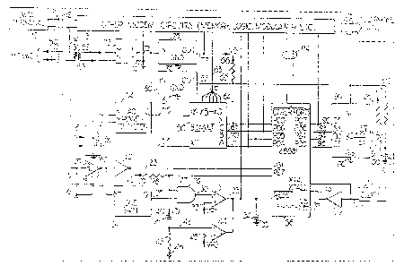
The drawing figure is a schematic diagram
of the preferred embodiment of the present invention.
Detailed Description
Turning to the drawing, the preferred
embodiment of the present invention will now be
described. The figure is a schematic diagram of the
present invention in a modem.
;3
- The preferred embodlment is included in a
modem 12 cons~ruc~ed around a microproce~:~or 36~ In
the preferred embodiment micEoprocessor 36 is the
Z8681, which is the eight ~egahertz ver~ion of the Z8
5 microproce~sor. De~ails of the oper~ti on and
internal structure of the microproces~or 36 ~re
available in 'cl~e literature ~upplied by the
manufacturer, Zilog, Inc. of cupertlno, Cqlifornia.
kSicroproce~sor 36 interfaces with other devices
lO through four eight-bit ports de~ignated by the
manuacturer as ports 0 through 3. This port
notation, along with the bit number, i8 used in
the figure to c~pecify a particular terminal o
microprocessor 36. For example, the de~ign~tion P20
15 refers to port number 2, bit number 0.
Before beg1ns~ing the de~ailed description
of the present inven~ion the environment of the
preferred embodiment will be d~3cribed. An external
data terminal 10 0 which may be a digital computing
20 machine or som~ oth~r digital device, communicates
with and is connected to the modem 12 by an RS-232C
interface ll. The modem 12 is also connec'ced to a
subscriber telephone line llS so that data may be
exchanged with some remote deviceO It will be
25 appreciated that the nu~ber of conductors in
telephone line 115 will be two or more, depending
upon the particular u~er ' s telephone sy~3tem. The
modem 12 con~rerts data from an RS-232C format to a
format ~u itable for tran~mis-~ion over a elephone
30 line 115, and vice ver~a.
I n~ ide t he modem 1~, the RS-232C ~us 11 and
the 'celephone line ll5 are conn~cted ~.o the other
modem circuits 13~ ït will be apprec:iated ~hat the
14
_ other modem circuits 13 compri~e~ for example, ~ignal
input and output conditioning and i~olation circuit~,
voltage regulator~ and filter~, pha~e locked loops,
modulators, demodulator~, ~t~tus indicator~,
S frequency yn~he~izers, and ~ read only me~ory ~ROM~
whir~ contains the fac~ory def~ult setting~ and ~l~o
the operating in~truction~ for microproces~or 36.
Microproces~or 36, hereinafter called
proce~Yor 36, co~municate~ with ~nd controls the
other modem circuit-q 13 by conductors 67, 70, 71, 92,
a ~ix conductor bu~ 63, and multiconductor bu~ 114.
~he number of conductor3 in bu~ 114 will neces~arily
depend on how many of ~he o~her por~ of proce~or 36
are required to implement the desired mode~ functions.
Exemplary details of how other func~ion~ of a modem
may be controlled by a microproce~sor ~uch ~g
proce~sor 36 may be found in U.S. Patent No~.
4,431,867 and 4,504,802 ~hich ar2 a ~igned to the
a~ignee of the pre3ent invention.
The proce~sor 36 i9 driven by a 7.9872 M~z
clock 110 which i~ connected by conductor 111 to the
XTAL1 terminal of proces~or 36 and to the input of an
inverter 112~ The output of the inverter 112 i~
connected hy conductor 113 to the X~AL2 termlnal o
processor 36.
At thi~ point a di~cussion of the function
o the data terminal ready (DTR) Rignal i~
appropriate~ The RS-232C bus 11 contain~ among other
conductor~ a DTR conductor 14. A data terminal 10
will place a ~true~ or active ~ignal on DTR conductor
14 when the data terminal i8 ready to exohange data
ov~r telephone line 115 via mode~ 12. If the DTR
signal i9 ~false~ or inac ive then the data terminal
10 i~ not ready to exchange data but may, if the data
terminal 10 ha~ asynchronous operation cap~bility, be
~z~
ready to 1~ue commands to the modem 12. The
re~pons~ of the modem 12 to the DTR sign~l i9
program~ed by the u~er frosn a~ynchronous data
terminall 10. Methods of accompli~hing thls are well
5 kno~m.
If the data t~r~inal 10 i3 a synchronous
datzl t~rm~ n~l a f al~a-to-true tranait~on of the DTR
sign~:l may isl~truct the ~ode~ 12 to go off-hook, dial
a ~elephone number ~ and the!n ~n~er èb~ ~yne~rol~ssus
10 mod~" The modem 12 will then be unre~pon~iv~ to
com~andl~ and will function as a d~ta com~unic~tlon21
devi~2 ~h~ch transfers d~ta bet~e~n the data lerminal
10 and the telephor~e line 115.
A true-to-false ~ran~it~on of l~he DTR
15 signal may then in~truct the modem to go on-hook arld
ent~r the a~ynchronou~ co~and mode. As i8 explained
below, the pre~ent ~nvention al~o per~l~ a
true-to-fal~e tran31tion of the DTR sign~l to
instruct the modem 12 to enter the ~dumba
a~ynchronous mode wherein ~he mode~ 12 i~
unre~pon31ve to com~and~ fro~ the data terminal.
If the data t~rminal 10 ig an a~ynchronous
data terminal then a fal~e-to-true transition of the
DTR ~lgnMl, occurring subsequent to a dial command
sent ~ro~ the data terminal 10, in~truct~ the modem
12 to coll3plete the telephone connection and enter the
asyns:bronotl~ data mode. ~he modem 12 will then be
unreapon~ive to commands and will function as a data
communication~ device which transfers data between
the data terminal 10 and the telephone l~ne 115. The
true-to-false tran~i~ion of th~3 DTR ~ignal m~y then
instruct the modem 12 to go on hook and ch~lnge from
the asynchronous on-line data tran3fer mode to the
a~ynchronous command modeO A~ i9 explained below,
the pre~ent invention al~o per~its a true-to-false
4~
16
tran~ition of the D1'R signal to instruct the modem to
enter the "dunlb" a3ynchronous mode.
A modem generally detect~ a change in the
DTR signal by periodically ~ampling it. However, if
5 electrical noi~e or a ~tatic dlsch~rge has caused the
microproces~or to lock up then the modem wlll ns:~t be
able to sample ~he l)TP~ signal and will s~ay locked up.
The pref rred embod$men'c use~ ~lectronic hardware
exlternal to processor 36 ~o detect ~he true-to-alse
10 change in the DTR signal and rese~ ml~:roproces~or 36.
This allows the user to regaln s:olltrol of the modem.
The data terminal ready ( DTR ) ~ ignal
conductor 14 of R5-232C bus 11, 18 connected to one
terminal of a capacitor 15 and to the input of an
15 inverting l~ne receiver 20. The response control of
lin~ receiver 20 i~ connected to one terminal of a
capacitor 17 by line 18. The other terminal~ of
capacitors 15 and 17 are connected b~ conductor 16 lto
the system ground. Capacitor 15 is a high frequency
20 noi~e suppre~sor and capacitor 17 shapes the respon~e
o line receiver ;20'7 Lin2 receiver ~0 converts the
DTR signal Otl conductor 14 from PcS-232C level~ to, in
the preferred embodiment, CMOS loyic voltage le~rel~.
The output of line receiver 20 i~ a negate~
2~ DTR signal and i~ connected by conductor 21 to the
input of inverter 22 and 'co the trigger input of a
po3 itive_adge_tr iggered, non-retr iggerabl~ one-shot
24 . The output of invert~r ~2 is the DTR ~ ignal and
i~ connected to the P31 input of proces~or 36 by
30 conductor 23. Proce~sor 36 can therafore detect the
false-to-true transition of the DTR signal by
periodically ~ampling the DTR signal on conauctor 23.
One-~hot 24 ha~ a period of approximately
2. 3 milliseconds . This period i8 not critic~l but,
35 a3 will be di~cu~sed belowJ must be long enough to
17
allo~ comparator 31 to discharge capacitor 34 and
cau~e a re~et of proce~sr)r 36. Methods of
construction of one-shot 24 are well known.
~ true-to-fal~e transltion of the DTR
s Rignal on eonduc~or 14 wlll be a fal~e-to-true ~lgnal
on conductor 21, thereby 'criggering one-~hot 24. $he
ta output of one-~ho~c 2~ i8 connec~ed by conductor ~5
to one input o a two-input A~aD-gate 26. The other
input o~ ~ND-gate 26 i~ connected by conductor 27 to
one terminal of a pullup re ~tor 28 ansl to ~he P27
ou~cput of proce3~0r 36. The other ter~ln 1 of pullup
resi~'cor 28 i~ connected to a loglcal 1 by conductor
29 .
If the u~er has programmed the modem 12 to
ignore the DTR ~ignal then proce~or 36 ~ill pla~e
logical 0 onto co~ductor 27, thereby disabling
AND-gate 26 and preventing the ou~put of one-~hot 24
from cau~ing a ra~et of processor ~. Conversely, if
the u~er ha~ programmed the mode~ 12 to be re~ponsive
to the DTR signal then proces~or 36 will place a
logical 1 on conductor 27, thereby enabling ~ND-gate
26 and allowiny a reset to occur.
The output of AND-gate 26 i~ connected by
conductor 30 to the inverting input of open collector
co~parator 31. The non-inverting input of comparator
31 i~ connected by conductor 32 to a f irst voltage
reference~ U~l. Voltage VRl is ~uch th~t a logical 1
on conductor 30 cau~e~ the output of comparator 31 to
be a lo~ical 0, and a logical 0 on conductor 30
cause~ the output of comparator 31 to be an open
circuit . In the pre~erred embodiment, the log ical
voltage i8 f ive volts and VRl 1~ approx~nately 2 .1
volt~ .
~he OUtp~lt of comparator 31 is connecte~ by
conductor 33 to ~he oth@r mode~ circuit~ 13, the
~z~
18
output of comparator 44, one terminal of a capacitor
34, and the negated re~'c lnput of proces~or 36. 'rhe
other terminal of capacitor 34 i~ connected to ground
by conductnr 35.
s If the DTP~ ~ignal on conductor 14 change~
from a true to a fal~e, the neg~ted DTR signal on
-onductor 21 wlll change from a logical 0 to a
logi~al 1, triggering one-~hot 24, and cau~ing it~ Q
output to become a logical 1 for ~pproxlma~ly 2 . 3
milli~cond~ . I f the u~er h~ progr~l~med the ~ode~
12 to be re~pon~3; ve to DTR commands, then the P27
output of proce3~0r 36 on conductor 2 7 wi 11 be a
logical 1, which enable~ AND-gat~ 26. 3ince the Q
output of one-~hot 24 i~ ~ logic~l 1, the output of
~ND-gate 26 will be a logical one, and 'che output of
comparator 31 on cor~ductox 33 will be a logical 0,
thereby discharging cap~citor ~4 9 and re~etting
proce~sor 36~ Approxi~ately 2.3 millisecond~ later
the Q output of one-shot 24 will revert to a logical
0, thereby cau~ing tha outpu~ of comparator 31 to
become an open circuit.
Proce~or 36 ha3 an internal lûO kilohm
resi~tor 37 connec'ced between the negated re~et input
and the ~upply voltz~ge V50 Therefore, once the
output of comparator 31 ha~ become an open ~ircuit
capacitor 34 will begin charging through internal
re~i~tor 37. When the voltage across capacitor C34
ha3 risen to approximately 3.1 volts, the reset of
proc,~ssor 36 will end. In the preferred embodiment
capacitor 34 i~ 3.3 microfarad~ This value i5 not
critical but must, together with the internal
re~istance at the RE:SET input, provide a time
constant which i~ long enough to allow processor 36
and the other modem circults 13 to re~et~ and short
enough that the modem 12 is not disabled or an
~2~Z~
19
excessive period. In the preferred embodiment,
true-to~false change in the DTR ~ignal on conductor
14 will cau~e proGessor 36 to be held in a re.~et
condltioll for approximately 0 . 3 seconds .
It will be appreciated tha'c an open
zollector comparator ~uch a3 c:omparator 31 cannot
in~tantaneously discharge a large capacitor ~uch as
capacitor 34. It will therefore be under~tood that
the 2. 3 millisecond period of one-~ho'c 24 waa chosen
to allow the output of comp~rator 31 to rema:Ln ~ n a
s:onducting ( logical 01 3ta~e for a ~ufficient ti~e to
di~charge capacitor 34 .
Upon termination of t~e re~ perlod,
proces~or 36 read~ the conf 1gurat~on settlngs in
memory 90 and tes'c~ or the pre~ence of ~umæer 61 on
plug 60 to determine what ope~a ing state the modem
12 ~hou ld be placed in . From the abov~ discu~sion it
will be ~een that the u~er may program the modem 1
so that a true-to-false tran~ition of the DTR ~ignal
on cs~nductor 14 i~ detected without using proce~sor
36 to monitor the ~tatus of the DTR ~iyna}.
Processor 36 i~ of a type which requ ire~
its initialization rou'cin~ to re3ide within the fir~t
256 bytes of execu table code . This 256 byte~ of code
contain~ in~truc'cions for conf iguring the proces~or
36. It al~o contains instruction~ which read and
test the memory device 90, read the factory default
configuration profile in the read only memory in the
other modem circu its 13 if the memory device 90 i~
defective or mi~ing, read the location of the jumper
61, and perform any other in~'cructions ~ce~sary to
complete the initialization oi~ the modem 12.
A~ praviou~ly ~tatad, the negated re~et
ioput of proce~sor 36 and one terminal of capacitor
34 are al~o connected to the output of opsn collector
~2~
comparator 44 by conductor 33. The inverting input
of comparator 44 i~ connected by conductor 42 to one
terminal o~ capacitor 41 ~nd one terminal of resistor
43. The other terminal of cspacitor 41 is connected
s to the supply voltage V5 by conduc~or 40. The other
terminal of resi~tor 43 i~ connec~d to ground by
conductor 46. The non-inver ing input of comparator
44 is connected to a ~econd voltage referenc~ VR2 by
conductor 45.
It will be appreci~ted that capacitor 41
couple~ ti~e-varyi~g voltaqe~ from the power supply
voltage V5 to the inverting input of co~parator 44.
If ~upply voltage VS i3 a ~teady D.C. voltage the
volta~e on the inverting i~put of ~omparator ~4 will
be zero. Thi~ i~ below the lev~l of reference
voltage VR2 so the output of comparator 4~ w~ll be an
open circuit.
~ owever, power supply noi~e, ripple, ~nd
the power-on-transient voltage~ will be coupled by
capacitor 41 onto conductor ~2. If the e voltages
exceed voltage ~R2 then ~he output of comparator 44
will be a logical 0, there~y di~charging capacitor 34
and re~etting processor 36. In the preferred
embodiment t referance voltage VR2 i~ 0.2 volts. This
voltage i~ not critical but should be large enouyh to
prevent inconsequential noi~e and ripple from
re~etting processor 3S, and ~mall enough to cause
processor 36 to be reset when power is on and
significant noise or ripple is present which would
cause the modem 12 to operate in an unreliable or
erxoneous manner.
From the above discu~ion it will be
understood that proc~s~or 3S and the other modem
circuits 13 are automatically re~etJ wi~hout user
invention, when power i~ ~ir~t turned on, and al80
~2~
whenever the noi~e and ripple on the power supply i~
~ignificant enough to adver~ely affect the
re 1 i ab i 1 i ty of oper at i on of the modem .
It will also be understood that, ~ince
comparatvrs 31 and 44 sre in parallel ~ the output~ of
both comparators mu8t be an ope~ circuit to allow
proce~or 36 to change froDt the reset condi'tion to an
operatirlg conditionO
Data terminal 10 is connected to the other
modem circuits 13 by an RS-232C in~erface cable 11.
The other modem cir~uit~ 13 are ~:onnected to
proce~sor 36 by a multiconductor bus 114, conductor
92, conductors 67, 70, 71, and, through the
multiplexer 56, by conductor 63. One ~killed in the
srt will realize that the user will typically u~e an
asyrlchronous data term~nal 10 to ~end the
configuration parameter~ to the mod~m 12 over the
RS-232C interface 11~ It will al~o be reali2ed that
the~e configuration parameters are initially stored
in the internal registers of processor 36.
Proces~or 36 i8 al~o connected to a memory
device 90. In the preferred embodiment the memory
device 90 ;8 an X2444, manufsctured by Xicor~ of
Milpitas, California, The X244~ i8 a serial
input-~erial output memory device which ha~ a 16
bit-by-16 bit nonvolatile electrically alterable read
only memory (EAROM) overl~id onto a 16 bit-by-16 bit
volatile random access memory (RAM)~
T h e m e m o r y d e v i c e 9 0 s e r v e 3 a ~ a
non-volatile RAM and is therefore referred to as a
NOVR~M. It operates as follows. The NOVRAM 90 has,
ex~luding the power supply and ground terminal3, five
input termin~ls and one output tPrminalO The chlp
enable (CE ) input ( line 95 ~ i~ held at a logical 1
35 when ~ending in~trUctionC or d~ta to~ or r~ceiving
~L2~
_ information from, the NOVRAM 90. In~tructions to,
and any data to be s~ored in, the NOVRAM 90 are
provided, in ~erial format, to the data input (DI)
terminal (line 92). Data fro~ the NOVRAM g0 i8
provided, in serial format, on ~he data output (DO)
termin~l (line 94). Instructions and/or data are
clocked into/out of ~he NOVRAM 90 ~y the shift clock
~SR~ terminal connected to line 93~
The NOVRA~ 90 h~ a e~en-word inqtruction
~et. The six instructions of pri~ry intere~t for
the preferred embodiment write data into and read
data out of a particular RAM addre~, set and clear
the E~ROM write enable latch, ~ransfer (~tore) th~
RAM data into the EAROM, and transfer (recall~ the
EAROM data into the RAM. A logical 0 on the negated
recall (R~ put terminal (line 97) will al~o c~u~e
the data in the EAROM to be transferred in~o the RAM.
Furthermore, if the EAROM write enable latch ha~ been
~et, a logical 0 on the negated store ( ST ) input
terminal (line 103) will cau~e the data in th~ RAM to
be tran~ferred into the ~AROM. Additional details on
NOVRAMs ~uch a~3 the x24~a4 are available in literature
available from ~he manufac'curer~ of ~uch devicefl and
are known to tho~e skilled in th~ art.
Processor 36 is connected to the NOVRAM ~0
as follows. The P35 output o~ proce~or 36 i~
connected to the chip enable input o NOVRAM 90 by a
conductor 95. The proce~or 36 place~ a logical 1
onto the conductor 95 when proces~or 36 i~ sending
instruction~ or data to, or receiving data from, the
NOVRAM 90, and place~ a lo9ical O onto the conductor
95 otherwise.
The P07 output of proces~or 3~ is connected
to the data input of NOVR~M 90 by conductor g~. The
processor 36 provldes instruction~ and dat~, i.e. -
~Z9~
23
operzltlng parameter3, to the NOVRAM 90 over conductor
92. Proce~sor 36 is also connected to the other
modem circuits 13 by conductor 92 and can communicate
with the other modem circults 13 over conductor 92
S when the chip enable conductor 9S i~ in a logical 0
state O
The P24 input of the proces~or 36 i9
connected to 'che data output ter~ nal of the NOVRAM
by a ccnductor 94. Data, i.e~ - operatin~
paraane~ers, ~1:ored in the NOVRAM 90 ~re tran~ferred
to the proces~or 36 over the conductor 94.
The P36 output of proce~or 36 i~ connected
to the shift clock input of l~OVR~M 90 by conductor 93;
The shift clock frequency mu~t be 1.0 M~lz or les~ for
the X icor X24 4 4 .
In the preferred embodiment the YCC
terminal of the NOVR~ 9û i8 connected by a conductor
82 to a f ive-volt power supply f ilter and regulator
8û. The rem21inder of the ::ircuits in the modem 12
are connected to another f ive-volt power ~upply
filter and regulator 75, the output of which appears
on conductor 77. The di~charge time constant of the
power supply 80 i~ approxima'cely 10 milliseconds
greater than the dischar~e time constant of the power
~upply 75. The charging time constant of the power
supply 80 is less than or equal to the charging time
con~tant of the power supply 75.
The negated recall input (RE ) of the NOVRP.M
90 is connected by a conductor 97 to one end of a
capacitor 100 and to one end of a resi3tor 102. The
other end of resistor 102 i~ onnected by cond~lctor
82 'co the output of the power supply 80. The other
end of the capacitor 100 i3 connected to ground by a
conductor lOlo Resistor 102 ~nd capacitor 100 are
selected to provide a time constant of approximately
~Z6~
~4
_ thirty micro~econds. When A.C. power is first
applied to the modem 12, the negated recall input of
the NOVRAM 90 will be held low for a brief period
after power ha~ been applied to the NO~RAM 90. The
logical O on the negated recall input in~truct~ the
NOVRAM 90 to tran~fer the lnfor~ation contained in
the ~AROM into the RAM. There~or~, when the ArC~
power i~ fir~t applled, the configuratlon profile
which the u~er had pre~iously ~tor~d 1~ no~ rec~lled
into the RAM of ~he NOVR~M 90. It will be
appreciated that the proce~or 36 can th~ eopy into
its internal regi~ter3 the configuration profile now
stored in the NOVRAM' 3 volatile RA~.
One skilled in the art ~ill appreciate tha~
the end o~ re~i~tor 102 conne~ed ~o the output of
power ~upply 80 can~ in~ead, be connect~d to the
output of power supply 75 ~f power supply 75 ch~rge~
at the same rate or a slo~er rate than power ~upply
80.
When a NOVRA~ 90 is manuf~ctured, the
manufacturer will typically, a~ par of the te~t~ng
proces~, load at least the fir~t regi~ter of the
EAROM with alternatill~ 1 ' 8 and O'~. ~oweYer, as i9
explained below, if the proce~or 36 ha~ previou~ly
~tored a user-~elected configuration into the EAROM~
it will al~o have loaded the first regi~ter of the
EAROM with a predetermined bit pattern which i~
different than the alternating 1'~ and 0'~ bit
pattern.
In the preferred embodiment, after a re~et
of the proces~or 36 ha~ been completed, the proces~or
36 will read the content~ of the first regi~ter of
the RAM section of NOVRAM 90.
If th~ fir~t reglster of the RAM of the
NOVRAM 90 contains the pred~ter~$ned blt pa~tern then
the proces~or 36 wi 11 copy into it~ internal
regi~ters the content~ of the remaining RP~M
register3, which i~ the u~er programmed configuration
profile, and use th~3 profile a the active
s configur~tion profile. E~owever, if the irst
reg~ster of the RAM does rlot contain the
predetermined bit pzll:tern9 the proce~or 36 will then
load the factory set de~ault configuration profile
from the ROM in the oth~r mode~ circuit~ 13 into it~
internal regi~ter~, and u~e thi~ prof~ le ~8 the
active conf iguration prof ile .
The proce~3~or 36 will therefore in~ tially
use, as ~he active confi~uration profile, ~he
u~er-programmed configura!ltion profile in the E:AROM if
the content~ of the f ir~t RAI~ regi~ter are the
predetermined bit pa~tern and9 other~ise, the
processor 36 will u3e the factory ~et default
conf iguration prof ile in the RûM.
It will be appres:iated that te~ting the
fir~t regi~ter of the RA~ of the NOVRAM 90 also
allow~ the processor 36 to det~ct a defective or
mis~ing NOVRAM 90. Under those circumstance~,
prOCe~380r 36 al80 ~elect~ the actory ~et defsult
con~igurat10n profile.
It will be apprQciated that the uqer can
u~e an asynchronou~ data terminal lO to s~lect the
active configuration profile from the factory
~et default configuration profile, the
user-programmed conf iguration prof ile stored in the
EAROM of the NOVRAM 90, or may generate a new active
conf iguration prof ile .
The output~ of a ~tep-down tran~former 51
are connected to the input~ of the AC power detactor
54 by conductor~ 52 and 53. The Q output of AC power
detactor 54 i!3 a logical 1 when ~C power i9 present,
26
and a logical 0 when the AC power i~ removed or fail~O
Me~hod~ of constructing an AC power detector 54 are
well known. The Q output of the AC power detector 54
is connected by a conductor 55 to the X6 input of an
8-to-1 multiplexer 56. The X output of the
multiplexer 56 is connected by a conductor 6 4 to the
P20 input of the proce~sor 36 and to the V5 ou put of
the power 5upply 75 by a re~istor 65 and a conduc~or
66 .
A~3~ume that the user, using the data
terminal 10 ~ commands the processor 36 to copy the
active configuration profile in it8 internal
regi~ter~ into the NOVRAE~!I 90. Proces~or 36 will
place a logical 1 on the chip enable conductor 95,
place a clock signal on the shift clo¢k conductor
93, and send a command, in serial dsta formAt, over
the data input conductor 92, which instruct~ the
NOVRAM 90 to store the next 16 bits of data in a
desi~nated register in the RAM o ~he NOVRAM 90~
Prc)ces~or 36 repea'c~ this sequence until the complete
configuration profile has been ~tored in the 16
regiYters in the RAM o~ the NOVRAM 90. Proces~or 36
will al~o cause the above referenced predetermlned
bit pattern to be loaded into the fir3t register of
the RAM~
Processor 36 then, through multiplexer 56,
tests the Q output of the AC power detector 54. If
the Q output is a logical 1, the processor 36, in the
manner described above, send~ a command to the NOVRAM
30 90 to ~et the write enable latch, and then a command
to copy the content~ of the RAM into the ~AROM. The
u~er has thereby cau~ed a new configuration profile
to be ~tored in the EAROM. Also, the predetermined
bit pattern is now stored in the fir3t register of
the ~AROM,
~z~
I f, however, the Q output of AC power
detector 54 is a logical 0/ indicating that the ~C
power ha~ failed, the processor 36 send~ to the
~aovRAM 90 only a command to se'c the write enable
latch. The negated stvre input of the NOVRAM 90 is
connected to the output V5 of ~he power supply 75
through a re~i~ter 104 and a conductor 105.
Therefore, as the output V5 of power supply 75 . alls,
l~he negated ~tore input of the Nl:)~FtAM 90 will bacs~me
a loglcal 0. Since the proce~sor 36 h~a 3~t the
write enable latch of the NOVRA~ 90, a logical O on
the negated ~tore input instructs the NOVRA~ 90 to
copy the contents of the RPPt into the 13AROM.
Therefore, the user-programmed conf iguratis~n prof ile
and the predetermined bit pattern will be ~aved in
the 13AROM of the NOVRA~q 90 even ~f a power Eailure
occurs .
It will be apprecia'ced that the
in~truction~ which direct proce~sor 36 to perform
2~ these function~ are contained in the read only memory
~ROM ) of the other modem circuits 13 .
NOVRAM 90 Eequires ten milli~econd~ to copy
the contents o~ the RAM into the EAROM. Therefore,
a~ previously ~tated, the NOVRAM 90 has a separate
power ~3upply 80 which ha3 ~ di~charge tlme con~tant
which is at least ten milli~econd~ greater than the
time constant of the power ~upply 75. This
arrangement therefore provides the NOVRAM 90 with the
necessary operating power for an additional ten
milli econds af ter the QUtpUt of the main power
supply 75 falls and the negated ~tore ~ignal on
conductor 103 ha~ become a legical 0~
Altern~te embodiment~ of the present
invention may be con~tructed ~o th~t ln the event of
an AC power failure, the modem 12 retains the
~2~i2~
28
. conf iguration profile in u~e at the time of the power
failure. In uch embodiments the ROM in circuit~ 13
i3 programmed 50 that the proces30r 36 periodically
samples the Q output of the AC power detector 54.
If the processor 36 detect~ a logical 0 on the Q
output of the AC power detector 54, then proce~sor 36
set~ the write enable l~tch of the NOVRAM. Thi~
cau~e~ the ~onteslt~ of the RAM ~ectlon of memory 90
to be tran~ferred to the ~AR~M when line 103 goe~
1~ low.
From the foregoing it will be ~pprec~ated
that the following t~ming constralnt~ are u~ed in the
emobidments described aboveO In the event o~ a power
ailure, the ou~put of AC power detector 54 go~8 ~
first. The outputs of power supply regul~tor~ ~5 and
80 al30 begin to dropO Proce~or 36 i5 programmed ~o
that it~ polling of the input~ to mult~plexer 56 18
at a ~ufficient rate so that det~ction of a logical 0
output from power detector 54 and execution of the
20 pro~ram steps nece~ary to write a comm~nd 'co NOVRAM
90 setting the write enable latch will occur before
the output of main power supply 75 falls to a point
at which the processor 36 will no longer operate.
Once this is accompli~hed, NOVRAM 90 no
25 longer care~ if the main power ~upply ha~ di~charged
to ~ point at which it can no longer operate
processor 36. The di~charge time con~tant of
regulator 80 is longer than the corresponding
discharge time cons~ant of main supply regulator 75
3~ by a period at lea~t equal to the time' required by
NOVRAM 90 to make its RAM-to-E~ROM tran~fer in
response to an active Rtore ~ST) input ~ignal,
Therefore, in the ~econd embodimsnt
deYcribed above, the time constrain~ are ~uch th~t
35 the coniguration profile in u3e at the time of pow~r
~Z6;~
29
Eailure is alwayq ~tored in the EAROM section of
NOVRAM 90, allowing it to be recalled when pawer i~
re3tored. In the preferred embodiment, the
con~traint~ make ~ure th~t once a configuration
5 prof i le ha~ been ~tored in the NOVRAM R~ ~ection in
respon~e 'co a u~er comm~nd, it will dependably be
tran~ferred to the E:AROM sec~tion even if ~ powex
fail7lre occur3 ju~t after proces~or 36 ~rrite~ data to
the RAM ~ection.
Some u~ers, after f ~ rst programming the
slesired configuration profile lnto the EAROM of the
NOVRAM 90, with an a~ynchronou~ data terminzll 10,
will use the modem 12 exclu3ively with a de~ignated
da~a terminal 10 and will hav~ l~ttle or no need to
15 later change the u~er-progra~ea config~aration
profi1e. In ~uch a ca~e, or in a ~a~e wher~ the user
i~ not concerned if the modem 12 fail~ ~o ~tore the
new conf iguration profile if the ~C power fails, then
the AC power detector 54 may }:e omitted. In this
20 ca~e, the negated store pullup resis'cor 104 would be
connec'ced to the outpu'c o the NO~7RAM 90 power ~upply
80 instead of to the V5 output of the power ~upply
75 .
If the modem 12 i~ cons'cructed in this
25 modified manner, the negated ~tore input of the
NOVRAI~ 90 will fall with ~he output of the power
~upply sn ~o a ~tore operation will not be effected.
The NOVRAM 90 will effect a ~tore operation only if
the proce~or 36 i~ues to the NOVRAM 90 both a
command to ~et the write enable latch of the NOVRAM
90 and a ~tore com~and.
An alternate embodiment of the pre~ent
invention use~ s~nly an electrically alterable read
only memory (EAROM) for the me~ory 90. In Ithi~ case,
35 the memory 90 i~ preferably embodled in the form of
~i2~
the NMC9346/COP495 memory, manufactured by National
Semiconductor Corporation of San'ca Clara, California.
The NMC9346/COP495 ha~ only an EAROM, and no RAM. An
implementation of the present invention uslng the
NMC9346/COP495 would be a~ ~hown in the figure
except that conduc'cors 97, 101, 103 and 105,
re~l~tors 102 and 104, and c~pacitor 100 are deleted.
Since thelr only purpose i5 to enable RAM~to-EAROM
and EAROM-to-RAM data transfer~, and ~ince the
NMC93416/COP495 doe~ no'c have a RP~M, these component
are not requ ired in the alternate embodim~n~. Al~o,
the maximum frequency of the shift clock ~ignal SS~)
i~ 250 kEIz. The principle~ of operation of the
N~C9346/COP~l95 are the ~ame a~ for th~ Xicor X2444.
Details on the NMC9346/COP495 are ~upplied in
li erature available from the manufacturer.
If the alternate embodiment is used and it
is desired that the current configuration profile be
automatically stored if a power failure occurs, then
power supply 75 mu3t have sufficient ~torage capacity
to permit the proce~or 36 to ~tore the complete
conf iguration profile into the memory 90 before the
output of power ~upply 75 drop~ to a point where the
pr oc e3 ~or 36 fails to function reliably.
Furthermore, the power supply 80 muRt maintain the
proper operating voltage for the memory 90 for at
lea~t 10 millisecond~ after the la~t store command.
The X7 input of multiplexer 56 i~ connected
by conductor 57 to the number 2 pin of a connector 60.
The number l pin of connestor 50 i~ connec~ed to
ground by conductor 62. The number 3 pin of
connector 60 i~ an open circuit. Jumper wire 61 can
be used to connect together either pin~ l and 2 of
connector 6û, or pin~ 2 and 3 of connector 60.
35 During the initialization period after th~
h940
termination of a re~et ~ignal on conductor 33,
proce~sor 36 sampleq the position of jumper wire 61
by commanding multiplexer 56 to connect its X7 input
~conductor 57) to its x output (conduc~or 64).
If jumper wire 61 connects pin~ 1 and 2 of
connector 60~ conductor 57 ~ill be connected to
ground and the X output of mult~plex~r 56 will be a
logical O, which command~ proces~or 36 to operate ~he
modem 12 in the "dumb~ mode. When the modem 12 i~ ~ n
the dumb mode it op~rate0 a~ a data tran~fer device
and iR unrespon~ive to commands from dat~ terminal
10, with the selectable exception of re~ponding in a
preprogranuned manner to change~ in the l)TR slgnal on
conductor 14. When the ~odem 1? ia in th~ dumb mode
the active- configuration param~ters are the
configuration para~ter~ preprogrammed into ~h~
NOVRAM 90 and cannot be chang~d. It will be
under~tood that the configur~tion parameter~ and the
response to the DTR signal on conductor 14 must have
been programmed using a data terminal 10 before the
modem 12 wa~ placed in ~he dumb mode.
If jumper wire 61 doe~ not connect pins 1
and 2 of connector 60, when processor 36 command~
multiplexer 56 to conn~ct it~ X7 input to its X
output, conductor 57 will ~ee an open circuit and
pullup re~istor 65 will pull conductors 57 and 64 to
a logic 1. This command~ proce~or 36 to operate
modem 12 in its intelligent mode.
When the modem 12 is in the intelligent
30 mode and i s also in the asynchronou~ state, processor
36 re~ponds to command~ from data terminal lO,
thereby allowing the user to change the conf iguration
parameter~ .
It wi ll be appreciated that the use of a
connector 60 and a jump~r wire 61 in~ide a modem 12
~26;~
ha~ ~everal advantage3. Assume, for example, that a
software command from data terminal were to be used
to command a modem to operate in the dumb mode. Once
the command is given, the modem cannot be commanded
to operate in the intelligent mode becau~e, once in
the dumb mode, the modem ignore~ all programming
commands f rom the data terminal. The s~od~m would
therefore be permanently locked in~o the dumb mode.
Of course, a switch could be used to ~elect
dumb/smart operal~ion. ~oweYer, in a co~mercial u~e
erlvironment where the modem 12 is just proyrammed
with an a~ynchronous data ter~inal and thereafter
u~ed only with a ~ynchronou~ data terminal, an
operatnr ma~Y inadvertently or mi~guidedly change the
~witch setting from dumb mode to ~mart mode. A later
data transfer could then erron20u~1y ~e interpreted
a~ a com~and to change the ~onfiguration. This would
render the modem u~eles~ until the configuration
parameters were reprogrammed, causing 108t time and
pos~ibly lost data.
~ n internal switch would reduce but not
entirely eliminate the above problem. Furthermore,
switche~ are susceptible to contact corro~ion from
atmospheric elements, thereby creating the
pos~ibility that contact corro~ion could create an
open circuit, thereby causing the modem to
unexpectedly enter its intelligent mode, with the
con3equences described above. The use of a connecter
60 and a jumper wire 61 therefore avoids these
problem~.
From the foregoing it will be appreciated
that the pre~ent inYention provides signif icant
improve~ent~ and advantages over prior modems. The
pre~ent invention provide~ for the automatic ~torage
and recall of a complete u~er-programmed
configuration profile in a nonvolatile memory, for
the automatic testing of the nonvolatile memory, and
for automatically ~witching to a factory set default
configuration profile ln the event that the
s nonvolatile me~ory i~ mis~ing, defective, or has not
been programmed with a conf iquratlon prof ile . The
pre~ent invention al~o automatically re~ets the m~dem
to a known operating ~tate if disruptive tran~ients
appear on the po~er ~upply or if a neg~tive
10 tran8ition of the D~R ~ignal occur~. The preRent
invention also provides a ~imple, effective method of
placing the modem into a dumb opera~il g mode ~o that
a defective da~a terminal canllot affec~ the
user -programmed active cc>nf iguration prof ile .
While thi~ invention h~a been described i~a
det2lil with particular re~erence to the pref~rred
embodiment thereof, it will be appreciated that,
because of the teachings contained herein~ numerous
variations and modif ications within the spirit and
20 scope of the pre~ent invention may ~ugge~t th~m~elves
to tho~e skilled in the art. Accordingly, thi~
invention i~ to be limited only by ~che claim~ below.