Note : Les descriptions sont présentées dans la langue officielle dans laquelle elles ont été soumises.
- 1 - 2~lO~-80~8
"Camera for recording television, photographic or cinematographic
images".
The invention relates to a camera for recording tele-
vision, photographic or cinematographic images, including a solid-
state image sensor designed as a charge transfer device comprising
a pick-up member, a storage member and a parallel-in, series-out
shift register member coupled to at least one sensor output termi-
nal, sai.d storage and shift register members being shielded from
incident light and said pick-up member being shielded over a strip
Erom incident light, said camera having a control circuit for the
image sensor for obtaining a-t the sensor output terminal a picture
signal having a periodical picture information associated with a
scene to be recorded and a dark current information originating
from below the said strip, said picture signal being obtained
after a picture information lntegration period in the pick-up
member and a charge transfer period for the transfer bet~een pick-
up member and storage member.
A camera of -this type, particularly for television has
been described in an English language -technical publicati.on
no. 150 of the Philips Electronic Components and Materials
Division, issued on 11 January 1985, in which the solid-state
image sensor is designed as a so-called frame-transfer sensor
which i.s mentioned as an attractive alternative to the television
camera tube. In the case of a colour recording based on -three
primary colours, the shift register member has three parallel
shift registers each applying a picture signal corresponding to a
colour to one o:E three output terminals. The dark current
6~3
- 2 - 2~)10~-805~
information originating from below -the said shieLding strip in the
pick-up member occurs in all three picture signals.
Apart from an embodiment of the control circui-t for the
image sensor, the said publication does not provide any circuit
information relating to the required adjustments in the camera.
Such adjustments are aimed at, for example, camera lens focusing,
picture signal black level setting for which the dark curren-t
information is utilized, white balance setting in colour recording
with three picture signals, e-tc.
It is an object of the invention to provide a camera
including the described solid-state image sensor with automatic
adjustments influencing the normal picture signal generation as
little as possible and being periodically performed in the correct
manner. To this end a camera according to -the invention is
characterized in that beyond the said picture information integra-
tion period and subsequent charge trans-fer period and after an
adjustment action information integration period in -the pick-up
member the control circuit for the image sensor is operative Eor
obtainlng at the sensor output terminal a signal having sequen-
tially the adjustment action information and the associated dark
current information.
Thus it is achieved that with an accceptable decrease of
the picture information integration period the result of the
adjustment action can be determined in an accurate manner from the
obtained adjustment action information and its own a~sociated dark
current information. In fact, as is required for performing a
current black-level clamping, this dark current lnformation of its
~, ~ .,
.5
~ 3 - ~010~-~058
own i.s more or l.ess proportional to -the period when the adjustment
action inEormation is present in the pick-up memberO It is then
possible within a ma~imum possible period to select the integra-
tion period for the adjustment action information in a flexible
manner and as desired, ~hilst its own dark current information is
automatically obtained.
An embodiment of a camera according to the invention in
which a desired information addition is present after the adjust-
ment action information integration period and which leads to a
minimum possible decrease of the picture information integration
period is characterized in that in the camera having a time signal
genexator comprising the control circuit for applying distinct
clock pulse signals to various outputs for the informati.on trans-
fer in and between the parts of the image sensor, the pick-up
member and the storage member are coupled to distinct clock pulse
outputs during a transfer period with an information -transfer
between the pick-up member and the storage member, said period
succeeding the adjustment action information integration period,
the frequency of the clock pulses for the information transfer in
the pick-up member being a factor higher than that in the. storage
member during at least part of the transfer period, the informa-
tion between the pick-up member and the storage member being
transferred under the control of the clock pulses for the informa-
tion transfer in the storage member.
In this case the information may be added for the
adjustment action information and for the dark current information
to -the same or a different extent dependent on a constant or
changing factor, respectively.
- ~ - 20:L0~-805~
In order to generate a picture signal and a signal with
the adjustment action information, which do not disturb each
other, an embodiment of a camera is characterized in that the
camera has a period setting circult through which the control
circuit for the image sensor is operative for generating the pic-
ture information or for genera-ting the adjustment action informa~
tion, both with the associated dark current information genera-
tion, said period setting circuit having an inpu-t for applying a
television field or picture synchronising signal, respectively.
In order to obtain an optimally separate signal proces-
sing relating to the picture information and the adjustment action
information, an embodiment of the camera is chara~teri~ed in that
at least one sensor output terminal is alternately coupled to a
first black level control circuit for the picture signal and to a
second black level control circuit for the signal comprising -the
adjustment action information and the associated dark current
information.
In order to per~orm a given camera adjustment an embocli-
ment of the camera i9 characterized in that a focus control
circuit succeeds the second black level control circuit for the
said signal for automatically adjusting an optical lens system
present at the camera and being positioned in front of the pick-up
member of the image sensor.
For a further camera adjustment an embodimen-t of the
camera is characterized in that in the camera suitable for colour
recording a white balance control circuit succeeds the second
black level control circuit for the said signal, which white
~i2~
- 5 - 2010~-~058
ba]ance con-trol circuit has a storage circui-t for the ampllfica-
tion factors for an adjustable amplifier which succeeds the first
black level control circuit for -the picture signal.
The invention will be described in greater detail by way
of example with reference to -the accompanying drawing in which
Fig. 1 is a block diagram of an embodiment o~ a camera
according to the invention,
Fig. 2 shows some diagrams as a function of time to
illustrate the invention,
Fig. 3 shows in greater detail an embodiment o-f a black
level control circuit suitable for the camera according to Fig. 1,
and
Fig. 4 shows a suitable detailed embodiment of a white
balance control circuit.
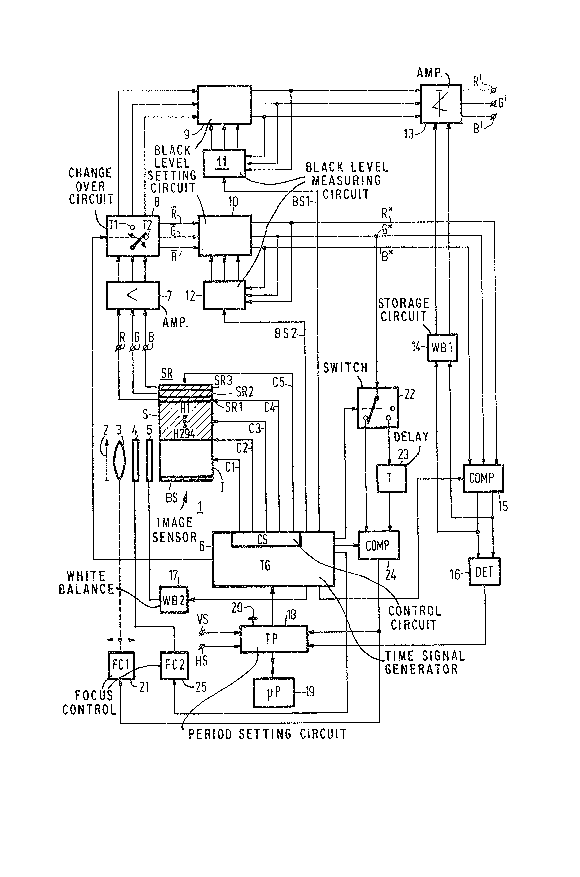
In the camera according to the inven-tion, which is shown
in a block diagram in Fig. 1, reference numeral 1 denotes a solid-
state image sensor, which, as is illustrated by means of a block
diagram, is in the form of a charge transfer device, ~ore specifi-
cally as what is commonly referred to as a frame transfer device.
The sensor 1 is in the form of an in-tegrated circuit comprising a
pick-up member I, an adjacent storage member S, which is shielded
from light, and adjacent thereto a parallel-in series-out shift
register member SR, which is also shielded from light and has
three output shift registers SRl, SR2 and SR3. The light shields
are shaded in Fig. 1 in which furthermore the pick-up member I is
provided with a strip-shaped shield BS. The cons-truction and the
operation under the control of clock pulse signals to be applied
.~
; r7
- 6 - 2010~-~058
is described in de-tail in United States Patent no. 3,~2~,337. The
pick-up member I and the storage member S are constructed from
pick-up and storage elemen-ts, respecti~ely, which are arranged in
rows and columns, a charge trans-fer occurring periodically in -the
column direction in -the members I and S and between them. In Fig.
l, ~l...H294 in the storage member S denotes that it is assumed to
comprise 294 rows of storage elements, which corresponds to 294
television lines H. The pick-up member I is also of a construc-
tion having 29~ rows of pick-up elemen-ts. Instead of providing
the row of storage elements Hl in the storage member S, it is
alternatively possible to use the shift register member SR for
that purpose as described in said Patent.
Instead of the described construction of the sensor 1
with the adjacent members I, S and SR, a storage member S arranged
in the integrated circuit under the pick-up member I may be used.
In this situation it should be ensured -that light incident on the
pick-up member I does not reach the storage member S and the shift
register member SR. The charge transfer from the pick-up member I
to the storage member S can now be effected directly from each
pick-up element to the subjacent storage element, whereafter the
charge transfer can be effected in the column direction in the
storage member S to the shift register member SR. It should be
noted that no charge trans,er between the pick-up elements in the
column direction is t'nen required. In the case in which this
feature is indeed present, it will become apparent from the
further course of this description that such a situation has i-ts
advantages.
"r .
- 7 - 20lO~-8058
A further example of a construction of the sensor 1 is
that in which the shift reglster SR i5 in the form of the base of
a comb which is shielded from light and whose teeth constitute
the storage member S. The pick-up elements of the pick-up member
I are arranged in columns between the teeth of the s-torage member
S. In this example the pick-up elements may have also a direct
charge transfer to the adjacent, associated storage elements. A
sensor having such a construction is sometimes referred to as an
inter-line transfer device. If also here it is possible to trans-
fer charge between the pick-up elements of the columns of the
pick-up member I, this will have apparent advantages.
For simplicity of description of the camera shown in
Fig. 1, the description will be based on the construction of the
sensor 1 in the form of the frame transfer device shown. To
control t~e sensor 1 it receives clock pulse signals denoted by
Gl, C2 to C5, which causes output terminals R, G and B of the
sensor 1, which are coupled to the outputs of the shift registers
SR1, SR2, and SR3, respectively, to carry a colour picture signal
corresponding to red (R), green ~G) and blue ~B) coloured light
components oriyinating from a scene to be recorded. For ~he sake
of simplicity supply voltages for the sensor 1 and for further
components in the camera of Fig. 1 are not shown. Further more
for the sake of simplicity of Fig. 1 connection leads are shown
singularly, but they may have a multiple design in practice and
may comprise signal processing circuits.
According to Fig. 1 the scene information to be dis-
~6'~;5
- 8 - 2010~-8058
played originates ~rom a scene which is shown as an arrow and is
denoted by 2. Light coming ~rom the scene 2 is projected onto the
pick-up member I of the sensor l via an optical. lens-system 3
which for the sake of simplicity is shown as a single lens and
opti.cal partial blocking devices 4 and 5. The devices ~ and 5 may
be in the form oE rotating disc shu-tters or of electronically
controlled shutters which comprise, for example, liquid crys-tals.
Depending on a voltage to be applied across the crystal, the
crystal either entirely or partially transmits or blocks light.
When a scene is recorded the light originating from the
scene 2 results in the scene forming an image on the pick-up
member I of the sensor l. It is assumed that a colour strip
filter is present in front of the pick-up member I in one o~ the
known manners, which filter has strips transmitting red, green and
blue light. During a scene recording period the photons of -the
incident light produce an electric charge integration in each of
-the pick-up elements of the pick-up member I. q'he pick-up period
is identical to a l;.gh-t in-tegration period. To process the scene
information obtained by integration or accumulation in the pick-up
member I the clock pulse signals Cl to C5 are supplied by a time
signal generator (TG) denoted by 6, more specifically a control
circuit CS present therein for the image sensor l. For a detailed
structure of the various clock pulse signals reference is made to
the said publication as an example. To emphasize a control of the
sensor l in a form deviating from one aspect of the present inven-
tion, the clock pulse signals for the control of the charge trans-
~er in the members I, .S and SR (signals Cl, C3 and C5) and between
- g - 20104--805
the members I ancl S, S and SR (signals C2 and C~) are shown
separately. Under t~e control oE these clock pulse signals the
sensor 1 supplies the colour picture signals R, G and B represent-
ing a scene information to be displayed. In the case in which the
signals R, G and B, after having been submitted to further signal
processing opera-tions which are customary for television, are used
Eor television reproduction, the camera shown in Fig. 1 operates
as a television cameraO ~nother possibility is to process the
signals R, G and B into a signal suitable ~or cinematographic
reproduction so that the camera shown in Fig. 1 forms part of a
cine film camera as a pick-up member. A further possibility is to
process the signals R, G and B to form a photograph or a slide so
that the camera of Fig. 1 ~orms part of a photographic camera as
its pick-up member. Independent of the specific camera construc-
tion the camera shown in Fig. 1 may operate for black-white or
colour recording. In the case of colour display a plurality of
sensors 1 may be present instead of the embodiment shown in Fig. 1
with a colour strip filter and the three shift registers SRl, SR2
and S~3.
~ccording to Fig. 1 the colour picture signals R, G and
B are applied to a pre-amplifier 7 succeeded by a change-over
circuit 8. The time signal generator 6 applies a switching signal
to a circuit input of the circuit 8 so that its output are alter-
nately coupled to the signal inputs. It is assumed that during a
switching period Tl, the amplified colour signal R, G and B are
passed on to a black level setting circuit deno-ted by 9 and tha-t
they are passed on during a switching period T2 to a black level
- 10 - 20lO~-~058
setting circuit lO. In Fig. ~ which for the purpose oE illustrat-
ing the operation oE the camera according to Fig. 1 shows some
time diagrams as a func-tion of time t, the periods Tl and ~2 are
plotted. Fig. 1 shows that the circuit 10 receives colour signals
R, G and B for which a possible time diagram for a colour signal
R, G or B in Fig. 2 is denoted by R/G/B.
Together with a black level measuring circui-t 11, the
black level setting circuit 9 constitutes a black level control
circui-t (9,11) intended for the picture signals. The circui-t
~9,11) is operative with a Eeedback, whilst a dark current gating
pulse BSl for the picture signal is applied in known manner from
the time signal generator 6 to the measuring circuit 11. Fig. 2
shows a possible time diagram for the gating pulse BSl. Similarly
the black level setting circuit 10 and a black level measuring
circuit 12 to which a dark current gating pulse BS2 (Fig. 2) is
applied from the generator 6 constitute a black level control
circuit (10, 12) which is however, intended for the signal R/G/B
(Fig. 2) comprising an adjustment ac-tion information. Fig. 3
shows a pos~ible embodiment of a black level control circuit (9,
11) and/or (10, 12) more particularly ~or the latter. While a
signal R, G or R (the signal R/G/B of Fig. 2) is supplied, the
circuit 10 supplies a signal RX, Gx or Bx which is denoted
b~ RX/Gx/B~ in Fig. 3.
An adjustable amplifier 13 applying signals R' G' and B'
to three outputs succeeds the black level control circuit (9, 11)
for the picture signal. It will be evident Erom the following
description -that the signals Rl, G' and B' are adjusted picture
signals which have been adjusted as an example for a focus setting
o~
- 11 - 2010~-8058
FC and a whlte balance setting Ws.
For the white balance setting ws two inputs of -the
adjustable amplifier 13 are connected to outputs o~ a storage
circui-t (W~l) denoted by 14 for -the a~plification factors in the
adjustable amplifier 13. Together with a comparison circuit 15
(COMP) to which the signals RX, Gx and sX are applied and a
detection circuit 16 (DET) succeeding it, the storage circuit 1
consti-tutes a white balance con-trol circuit (14, 15, 16), a
possible more detailed embodiment of which is shown in Fig. 4. A
signal which is not ~urther indicated is applied from the time
signal generator 6 to the comparison circuit 15 to determine the
period of operation of -the white balance control so as to achieve
an optimum white balance setting WB which is detected by the
circuit 16. In this case the semi-blocking device 5 which is
controlled through a control circuit 17 (WB2) from the time signal
generator 6 can be used. The device 5 can alternately pass light
originating from the scene 2 in an unimpeded manner and via a
plate of, as it were, frosted glass. During the presence oE the
frosted glass pla~e in the optical path so that the scene informa-
tion is mainly non-coloured and is more or less evenly picked up
by the sensor 1, the white balance setting WB is adjusted. After
the optimum setting has been achieved, the detection circuit 16
applies a signal to a period se-tting circuit (TP) denoted by 18
which controls the time signal generator 6. Input and output
leads of the circuit 18 are connected to a microprocessor (/uP)
denoted by 19. A television field or picture synchronising signal
VS and a television line synchronising signal HS are applied to
- 12 - 2010~-80~
the circuit 18. Near the circuit 18 there i~ shown an adjustment
and setting hutton 20 through which a given adjustment action
programme can be selected or composed. The programme is fixed in
a manner to be arbitrarily adjusted in an adjustment ac-tion
con-trol unit thus :Eormed (18, 19).
For the purpose of adjusting the focus set-ting FC in the
optical system of lenses 3, this system is coupled to a rocus
setting circuit (F~l) denoted by 21. For the focus set-ting FC -the
signal Gx is used which i5 applied directly through a change-
over circuit 22, and through a delay circuit 23 (T) to a compari-
son circuit (COMP) denoted by 24 which precedes the focus setting
circuit 21. The time signal generator 6 applies signals not
further indicated to a circuit input of the change-over circui-t 22
and to an input of the comparison circuit 24 for fixing the perio-
dical period of a signal comparison~ Due to the fact tha-t the
output signal from the comparison circuit 24 is applied to the
period setting circui-t 18, this circuit ascertains whether an
optimum focus setting has been achieved, whereupon the focus
adjustment b~ means of a focus control circuit (22, 23, 24) thus
formed is still switched on periodically, but does not have any
consequences for the focus setting circuit 21. The periodical
switch-on of the relevant adjustment is, for example, fixed in the
action programme which is presen-t in the adjustment action control
unit (18, 19). This makes it possible to perform a periodical
inspection of the adjustmentsO
Several adjustment actions may be considered for adjust-
ing the focus setting FC. There is a possibility to have a camera
~-
:1~6~
- 13 - 2010~-~058
construction with an addttional periodically operative infra-red
source detecting the infra red radiation reflec-ted by the scene 20
The optical semi-blocking device 4 is, for example, a filter in
this case which passes alternately scene light in an unhindered
manner and only received infra-red radiation. To thls end -the
camera of Fig. 1 is to be formed with a control circuit (FC2)
denoted by 25 through which the device 4 i9 controlled from the
time signal generator 6. Another solution is described in United
States Paten-t no. 4,3~1,523 in which the optical semi-blocking
device 4 is present for partially blocking the optical path. This
blocking action is effected alternately on first and second
portions of the optical path, which portions are situated in subs-
tantially mutually opposite positions on either si~e of a central
axes of the optical path. By partially blocking the optical path
two images are obtained via different portions of the optical lens
system 3. When focussing is at an optimum, the two images are
optimally in registration. A non-optimum focussing position
results in images which are shifted relative to each other, the
direc-tion of the shift depending on over or under focussing.
During the signal comparison operation with the aid of the circui-t
24 the fact that the two images are shifted relative to each other
is shown by a non-optimum signal correlation, and to obtain an
optimum signal correlation the focus setting is modified in the
correct direction through the circuit 21. The comparison circuit
24 receives the consecutively occurring adjustment action informa-
tion components simultaneously through the change over circuit 22
and the delay device 23. The change-over circuit 22 is shown in
~l~6f~3~i5
~ 14 - 2010~-~05~
Fig. l with a free contact for simple illustration o~ the switch-
off state of the -focus control circuit (22, 23, 24) wherl-the white
balance control circuit (]4, 15, 16) is switched on.
To illustrate the advantage o-f the camera of Fig. l
being able to operate with automatic adjustmen-ts which influence
the normal picture signal generation as little as possible and
which are performed periodically in the correct manner, reference
is made to Fig. 2. Fig. 2 shows a -television field period denoted
by TV in which in an interlaced system two or more field periods
constitute one picture or frame period. In a non-interlaced sys-
tem the period TV is also the picture period. The period TV
consists of a field scan period STV and a field blanking period
BTV. The reference VS' denotes a field blanking signal which has
been derived, for example, from the applied field synchronising
signal VS. Fig. 2 only shows the clock pulse signal C2 which
ensures the information transfer between the pick-up member I and
the storage member S of -the sensor l of Fig. l. Different periods
can be defined by means of the clock pulse signal C2. The refer-
ence IIT denotes a picture information integration period succeed-
ed by an associated charge transfer period ITT. An adjustmentaction information integration period i5 denoted by AIT succeeded
by an associated charge transfer period ATT. It appears that the
periods IIT, ITT, AIT and ATT combined cover one field period TV.
The re~erence C2S in Fig. 2 denotes a transfer signal comprising
the in~ormation transferred between the pick-up member I and the
storage member S. The transfer signal C2S is shown with some
information blocks, more speci fically a block with a picture
~6~
- 15 - 2010~-~05~
in~ormation II and an associated dark current information I~3I and
a block with an adjustment action inEormation AI and an associated
dark curren-t information A~I separated therefrom. Prior and
subsequent to the relevant information components AI and ABI in
the information block (AI, ABI) there is no information or there
is only inEormation which is not utilized and which i5 irrelevant
for the adjustment. To illustrate the information blocks (II,
IBI) and (AI, ABI) as they are present at given instan-ts in the
storage mem~er S of the sensor l, two images Al and A2 thereof are
shown in Fig. 2. In the firs-t image Al the picture information II
and the associated dark current information IBI fill the storage
member S completely. In the second image A2 the storage member S
still comprises a part of the picture information II, the conti-
guous dark current information IBI and the separated adjustment
action information AI and associated dark current information IBI.
Between the inEormation components IBI and AI of the image A2 a
broken line marks the instant when the period AIT ends. The
adjustment action information AI may occur in one or more tele-
vision lines in the storage member S and may originate from the
same numher of television lines of the pick-up member I. ~To
increase the contents of the adjustment action information, it is
possible to add up information by increasing the clock pulse
frequency of the signal Cl during the transfer period ATT by a
factor of for example several tens as compared with the clock
pulse frequencies of -the signal C2 controlling the information
transfer from the pick-up member I to the storage member S. As a
result information is added up in the row H29~ of storage elements
:~ ~6~
- 16 - 2010~-8058
in the storage member S because information is trans~erred between
the pick-up member I and t'ne storage member S once is as many
times as the frequency actor. A fre~uency fac-tor of forty is
mentioned as an example. Consequently the information of forty
rows of pick-up elements reaches a row of storage elemen-ts.
During at least part of the transfer period ATT the higher clock
pulse frequency factor may be present which applies relative to
the same clock pulse frequency in the signals C3 and C4. For the
information ABI which may be present in one row of elemen-ts of the
storage member S it i5 assumed that it may originate from, for
example, three rows of elements of the pick-up member I present
under the strip BS of the sensor 1 of Fig. 1.
The information can be added without any further
measures in the image sensor 1 when it is designed as a frame
transfer device. In the case of an embodiment with the described
underlying storage part or the described inter-line structure
there should be a possibility to have charge transfer between the
pick-up elements in -the column direction.
E'ig. 2 shows a time diagram of the dark current gatiny
pulse ~Sl for the picture information, which pulse covers, for
example, one or more line periods TH or a part of a line period
TH. The pulse BSl occurring in Fig. 2 over one line period TH is
present at the commencement of the field blan~ing period BTV.
During the preceding field scan period STV and the duration of the
pulse BSl which together constitute the switching peri.od Tl, the
pre-amplifier 7 is coupled through the change-over circuit 8 to
the circuit 9 so that the signals R', G' and B' occur in known
r3~5
- 17 - 2010~-805
manner at the correct black leve'l and t'he correct white balance.
Fig. 2 fur-thermore shows a time diagram of t'he dark
current gating pulse ~S2 for the adjustment ac-tion information.
During the swi-tching period T2 the pre-amplifier 7 is coupled via
the change~over circuit 8 to the circuit 10 in -this case. In
relation to the period T2 th~ adjustment action information AI and
the associated dark current information ABI are shown in the
signal R/G/B. The signal R/G/~ illustrates that after the preced-
ing adjustment action information integration period ~IT in the
pick-up member I each sensor output terminal R, G and B carries a
signal having sequentially the adjustment action informa-tion AI
and the associated dark current information ABI. In the circuits
10 and 12 the information ABI ensures a correct black level clamp-
ing relative to which the correct value of the adjustment action
information AI occurs in the focus control circuit (22, 23, 24) or
in the white balance control circuit ~14, 15, 16). The result of
the relevant adjustment action can thereby be determined accura-
tely.
In Fig. 1 the change-over circuit 8 is shown for obtain-
ing an alternate coupling of the terminals with the signa~ls RrGand B, with the black level control circuit (9, 11) for the
picture signal and with the black level control circuit (10, 12)
for the adjustment action signal. Instead of by using the change~
over circuit 8 the alternate coupling may be realised by means of
gating signals for the circui-ts (9, 11) and (10, 12) originating
from the time signal generator 6.
The following number are mentioned as e~amples. The
~Z6'~65
~ 20104-80S8
period ATT may comprise thirteen line periods TH divide~ into 5TH
without relevan-t inormation, lTH with the informa-tion AI, 5TH
without relevant information, lTH with the in~ormation ABI and lTH
without relevant in-formation. The preceding period ~IT may be
arbitrarily chosen dependen-t on the desired strength of the
adjustment action inFormation AI and on an addition of in-Eorma-tion
used to a greater or lesser extent. Once -the period AIT ~ ATT is
selected for a given use of the camera, this period is fixed
during use so that the period IIT does not change. Within the
period AIT ~ ATT the limit between integration and transfer may be
arbitrarily shifted or there may be several, separate adjustments.
In this case it is important to maintain the period AIT + ATT as
short as possible because this period is subtracted from the maxi-
mum possible picture information integration period which is
normally equal to the period TV - ITT. It is known that the
period ITT is chosen to be equal to 8TH with the optical path
being interrupted by the lens system 3 during the information
transfer to prevent signal smear as a resul-t of a continuing
information integration during the period ITT. It follows that
for the strength of the picture information generation a,reduction
factor occurs which is equal to the period IIT = TV - ITT - AIT -
ATT divided by the period TV - ITT. Although the optical inter-
ruption during the period ITT may or may not '~e effected, such an
interruption during the period ATT is necessary in practice in the
case of the focus adjustment. For the period T2 there may apply
that T2 = 7TH in which the information components AI and ABI may
each occur spreaded in lTH. The periods T2 and ITT combined
'~'~' .
- 19 ~ 2010~-805~
should be shorter that the field blanking period BTV for which in
accordance with television standards there may apply that BTV =
2lTH or BTV = 25TH dependen-t on the television standard with TV
= 262.5T~ or TV -- 312.5TH.
It follows from the foregoing that it is required to
perform field synchronisation for obtaining picture information
and ad~us-tment action information generations which do not disturb
each other. This synchronisation can easily be realised by apply-
ing the field synchronising signal VS to the period setting
circuit 18 of Fig. 1.
Fig. 3 shows an embodiment of the black level control
circuit (10, 12) which is sufficiently fast under the supply of
the signal R/G/B and the dark current gating pulse BS2 shown in
Fig. 2. An input terminal 30 is connected to ground via a cable
terminating resistor 31 and is furthermore connected to a (+)
input of a differential amplifier 32. A (-) input of the ampli-
fier 32 is connected via a feedback resistor 33 -to the output
thereof and is connected through a resistor 34 to the output of a
further differential amplifier 35. I'he (-) input of the amplifier
35 is connected to ground and the (+) input is connected,via a
transistor 36 to the output of the amplifier 32 and via a capaci-
tor 37 to ground. The transistor 36 is of the type having an
isolated gate electrode. A source electrode of the transistor 36
is connected to the (+) input of the amplifier 35 and a drain
electrode is connected to the output of the amplifier 32, whilst
the gate electrode is connected to an input 38 to which the gating
pulse BS2 is applied, The gating pulses BS2 have, or example,
- 20 - 20104-8058
pulses occurring from a negative vol-tage to the ground potential
wlth the period TH or a fraction thereof. The periodical pulses
of the period TH render transistor 36 conducting. The result of a
clamping circuit (32-38) thus formed is that the ground po-tential
during the period TH occurs at the output of the amplifier 32. A
deviation thereof which may be present at the beginning of the
period TH is corrected ~ecause the amplifier 35, which is opera-
tive as a differential amplifier, supplies such a current to the
(-) input of the amplifier 32 that the ground potential occurs at
its output.
The feedback clamping circuit (32-38), whose amplifica-
tion factor is equal to one, supplies the signal RX/Gx/Bx to
an output 39 for further processing -for the relevant ad~ustment.
Fig. 4 shows a possible embodiment of the white balance
control circuit (14, 15, 16) of Fig. 1. The respective signals
RX, Gx and Bx are applied via input terminals 40, 41 and 42
-to a ma-trix circuit 43 (M). The matrix circui-t 43 supplies, for
example, colour difference signals RX-Yx and BX-Yx for
which there applies that yx=0.3, Rx + 0.59 Gx + 0.11 BX.
The colour difference signals RX-Yx and BX-Yx are applied
via respective signal integration circuits 44 and 45 to (+) inputs
of respective differential amplifiers 46 and 47 whose (-) inputs
are connected to ground. The outputs of the differential ampli-
fiers 46 and 47 are connected to a switch-on/off circuit 48 which
i5 controlled via a circuit input from the time signal generator 6
of Fig. 1. The storage circuit 14 and the detection circuit 16
succeed the change-over circuit 48 which, together with -the compo-
9 ~
- 21 - 20L04-~058
nents 43, 44, 45, 46 and 47, consti-tutes the comparison circuit 15
of Fig. 1. Two output terminals 49 and 50 of the circuit 14 carry
voltages which determine the amplifica-tion Eactors of the adjust-
able amplifier 13 of Fig. 1. Upon detec-tion of the ground poten-
tial at both inputs an output 51 of the de-tection circuit 16 gives
the indication to the period setting circuit 18 of Fig. 1 that -the
white balance setting WB is at an optimum.