Note : Les descriptions sont présentées dans la langue officielle dans laquelle elles ont été soumises.
FJ-6297 ~,
CHANNEL-SYSTEM EXCHANGE SYSTEM FOR DIGITAL DATA
RADIO-COM~UNICATION SYSTEM
BACXGROUND OF THE INVENTION
1. Field of the Invention
The present invention relates to a communi-
cation system. More particularly, it relates to a
channel-system exchange system for a digital data
radio-communication system including at least one main
radio-communication channel system and a standby radio-
communication channel system, which the exchange system
is provided at a reception side of the main radio-
communication channel system and exchanges the mainradio communication channel system for the standby
radio-communication channel system and vice versa.
2. Description of the Related Art
In a digital data radio-communication system,
a channel exchange system is provided at the reçeiption
side of each main radio-communication channel system.
The channel exchange system exchanges a channel from its
main radio-communication channel system to a standby
radio-communication channel system when any device in
the main radio-communication channel system fails. The
channel exchange system also exchanges a channel from
the standby radio-communication channel system to the
main radio communication channel system when the failed
device is restored~ The channel exchange system also
exchanges a line when receiving data errors due to
fading are increased and restores the exchanged channel
when the errors are reduced. Due to ~he provision of
the channel exchange system, the reliability of the
digital data radio-communication system is improved.
In order to avoid loss of data during the
channel exchange, a high-speed semiconductor switch has
been employed in the channel exchange system. The
high-speed semiconductor switch may substantially
'' :''
: ' .
3:a~7
realize the high speed channel exchange without the data
loss during the exchange so far as the exci-ange of talk
data or the like, because one or two bit data loss does
not substantially affect a quality of th~ data. However,
the high speed channel exchange of the prior art, even
with a high-speed switch, cannot avoid loss of at least
one bit of data due to the phase difference between the
data received in the main radio-communication channel
system and in the standby radio-communication channel
system and/or pattern mismatch of serial data to paral-
lel data conversions at a transmission side in the main
and standby radio-communication channel systems. This
lost data will be described in more detail with reference
to sp~cific examples. When data to be communicated is
of the digital type used for a computer system or the
like, i.e., each bit having an important value and being
unable to be lost, loss of even one bit must be pre-
vented. Accordingly, prior art digital data radio-
communication systems having such high speed exchange
means cannot be applied to such digital data communi-
cation systems with a high reliability and a high
quality.
SUMMARY OF THE INVENTION
An object of the present invention is to provide a
channel exchange system for a digital data radio
communication which exchanges a channel between a main
radio-communication channel system and a standby radio-
communication system without loss of any bit of data and
with a high speed.
According to the present invention, there is
provided a channel-system exchange system for a digital
radio-communication system including at least one main
radio-communication channel system and a standby radio-
communication channel system, the channel-system exchange
system being provided at a reception side of each main
radio-communication channel system having a serial-to-
parallel data converter (S/PC~ converting serial data to
i3~
be transmitted to a first plural.ity of channel data on
the basis of a modulation method at a transmission side,
and the standby radio-communication channel system
having another S/PC having the same construction as the
S/PC and converti.ng the serial data to a second plurality
of channel data on the basis of the modulation method at
the transmission side.
The channel-system exchange system in each main
radio~communication channel system includes a first
exchange unit for exchanging a channel or channels of
the first channel data received at the reception side
of the main radio-communication channel system, a se-
cond exchange unit for exchanging a channel or channels
of the second channel data received at the reception
side of the standby radio-communication channel system,
and a switching control unit, operatively connected to
the first and second exchange units, for receiving
first data exchanged at the first exchange unit and
second data exchanged at the second exchange unit, and
for switching and outputting either the first data or
the second data on the basis of a channel-system ex-
change mode. The switching control unit detects a phase
match between the first data and the second data, shifts
either the first or second data defined by the channel-
system exchange mode until predetermined bit of data areshifted when the phase match is not obtained, and
activates either the first or second exchange unit
determined by the channel-system exchange mode when the
predetermined bit data shift is terminated. The acti-
vated exchange unit delays at least one channel datatherein defined by a first relationship based upon the
modulation method by one bit and exchanges the channel
data on the basis of a second relationship defined by
the modulation method. The switching control unit
repeats the phase match detection for the channel
exchanged data and switches either the received data on
the basis of the channel-system exchange mode when the
.
' ,
- .~l;26~
phase match is obtained~
The channel-system exchange system may further
include a switching judgment unit, operatively connected
to the switching control unit, for receiving the first
channel data and the second channel data, for judging
conditions of the main and standby radio-communication
channel systems on the basis of the received channel
data, and for outputting a signal indicating the channel-
system exchange mode determined by the conditions to the
switching control unit.
BRIEF DESCRIPTION OF THE DRA~INGS
Other objects and features of the present inventionwill be described below in detail with reference to the
accompanying drawings, in which:
lS Fig. 1 is a block diagram of a digital data
radio-communication system in which a channel system
exchange system of the present invention is applied;
Figs. 2a and 2b are graphs representing a
phase difference between a main radio-communication
channel data and a standby radio-communication channel
data in Fig. 1;
Fig. 3 is a block diagram of a serial data to
parallel data converter (S/PC) for four phase-shift-
keying modulation (PSK), shown in Fig. l;
Figs. 4a and 4b are graphs representing a
pattern match and a pattern mismatch of parallel con-
verted data at the S/PC shown in Fig. 3;
Fig. 5 is a block diagram of a channel-system
exchange system of the present invention shown in
Fig. l;
Figs. 6a to 6g are graphs illustrating the
operation of the exchange system of Fig. 5;
Fig. 7 is a circuit diagram of a switching
unit shown in Fig. 5;
Figs. 8a and 8b are graphs representing the
channel exchange by the switching unit shown in Fig. 7;
Fig. 9 is a detailed circuit diagram of the
.
i3~7
switching unit shown in Fig. 7;
Fig. 10 is a block diagram of an S/PC for
eight PSK;
Figs. lla to llc are graphs representing the
channel exchange for eight PSK data;
Fig. 12 is a block diagram of an S/PC for 16
quadrature amplitude modulation (QAM);
Figs. 13a to 13d are graphs representing the
channel exchange for 16 QAM data;
Fig. 14 is a block diagram of an S/PC for 64
QAM; and
Figs. 15a to 15f are graphs representing the
channel exchange for 64 QAM data.
DESCRIPTION OF THE PREFERRED EMBODIMENTS
Figure 1 shows a block diagram of a digital data
radio-communication system of the present invention.
The digital data radio-communication system includes a
plurality o~ main radio-communication challnel systems
and a standby radio-communication system. Each main
radio-communication channel system includes a switching
circuit SW, a serial data to parallel data converter
S/PC, and a transmitter T at a transmission side, a
channel, i.e. a data propagation path between the
transmission side and a reception side, and a receiver
R, a switching circuit SW, a channel-system exchange
system CH-EXCH, and a parallel data to serial data
converter P/SC at the reception side. The standby
radio-communication channel system includes an S/PC and
a transmitter T at the transmission side, a standby
channel LS, and a receiver R and a P/SC at the reception
side.
In a normal operation, each main radio-communioation
channel system, for example, a first main radio-
communication channel system, at the transmission side,
receîves a serial digital transmission data Tl, converts
the received serial di~ital transmission data through
the switchin~ circuit SW to parallel data at the S/PC,
:
:
3~
-- 6 --
and transmits ~he para]lel-converted data to the recep-
tion side through the channel Ll. At the reception
side, the irst maiTI radio-communlcation channel system
receives the transmitted data at the receiver R and
supplies the same to the P/SC through the switching
circuit SW and the channel-system exchange system
CH-EXCH~ The P/SC converts the received parallel data
to a serial reception data Rl. In the normal operation
state, the switching circuit SW in the transmission side
is energized to supply the transmission data Tl to the
S/PC. Also, the switching circuit SW in the reception
side is energized to supply the data received at the
receiver R to the channel exchange system CH-EXCH. Th~
channel-system exchange system CH-EXCH supervises the
quality of the received data. If the quality becomes
low, the channel-system exchange system CH-EXCH acti-
vates a control circuit at the reception side (not
shown) and also activates a control circuit at the
transmission side (not shown) through a channel (not
shown~. At the transmission side, the control circuit
deenergizes the switching circuit SW to supply the
transmission data Tl to the S/PC in the standby radio-
communication channel system. Simultaneously, at the
reception side, the control circuit energiæes the
switching circuit SW in the first main radio-
communication ehannel system to supply the data received
at the receiver R in the standby radio-communieation
channel system to the P/SC in the first main radio-
communieation system through the channel-system exchange
system CH-EXCH. As a result, if any device in the main
radio-communication channel system fails or the channel
is subjected to fading, the data communication may be
continued, When the device is restored or the fading
eliminated, the data communieation of the main radio-
communication channel system is restored from thestandby radio-communicatioll channel system by energizlng
the switching circuits SW at the transmission side and
-- 7 --
by deenergizing the switching circuit SW the xeception
5 ide.
The switching circuits SW at the transmission side
include high speed semiconductor switches each consist-
ing o~, for example gate circuits or switching tran-
sistors. Similarly, the switching circuits SW at the
reception side include high-speed semiconductor switch-
es. Accordingly, high speed channel data change at the
transmission side and the reception side can be achieved.
However, a simple channel data change is insuffi-
cient in digital data exchange, especially the exchange
of data used for computer systems or the like, due to
lost data. Loss of data may arise due to a phase
difference and/or pattern mismatch
The above phase difference is caused by a pxopa-
gation characteristic difference between the channel LS
of the standby radio-communication channel system and
the channel, for example, Ll of the main radio-
communication channel system. More specifically, if the
same transmission data is transmitted from the trans-
mitters T in the main radio-communication channel system
and the standby radio-communication channel system, data
RM-DATA, shown in Fig. 2a, received at the receiver R in
the main radio-communication channel system may differ
Erom data RS-DATA, shown in Fig. 2b, received at the
receiver R in the standby radio-communication channel
system, due to the propagation time difference between
the channel Ll and the channel LS. The data difference,
i.e., the phase difference, may be one or more bits of
data. A~ a time tSW shown in Figs, 2a and 2b, a
channel change is carried out, then a discontinuity of
data train results.
The pattern mismatch is caused by the timing
difference between the S/PCs in the main radio-
communication channel system and the standby radio-
communication channel system, as shown in Figs 3 to 4b.
Figure 3 shows a block diagram of the S/PC converting an
- 8 --
original transmission signal S-ORG of 32 MHz to two-
channel data each 16 MHz. Figure 4a shows ideal parallel
channel data MAIN and STANDBY converted from a same
serial transmission data at the S/PCs in the main and
standby radio-communication channel systems. However,
the parallel-converted data MAIN may be shifted by a
change of the conversion time, as shown at the top of
Fig. 4b. At this time, if the parallel-converted data
STANDBY, as shown at the bottom of Fig. 4bl is obtained,
or vice versa, and the channel change is made, pattern
misrnatch at the reception side cannot be avoided.
When such a phase difference and/or pattern mis-
match happens, a circuit connected to the P/SC of the
main radio-communication channel system may become
confused with the discontinuity of the data train or the
discrepancy of the received data, stop the data recep-
tion, thereafter restart the data reception after the
complete change of the channel. This substantially
means a system down state.
Preferred embodiments of the present invention will
now be described.
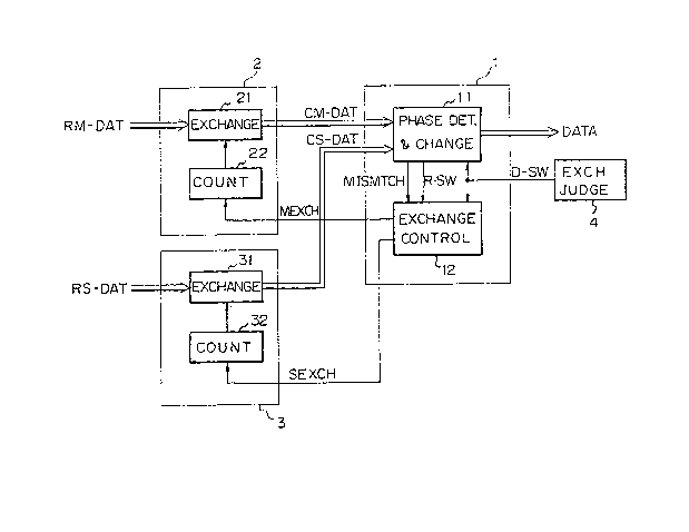
Figure 5 is a block diagram of the channel-system
exchange system CH-EXCH in Fig. 1~ The channel-system
exchange system includes a switching control unit 1
consisting of a phase detection and change circuit 11
and an exchange control circuit 12, a main exchange
unit 2 consisting of a main exchange circuit 21 and a
main counting circuit 22, a standby exchange unit 3
consisting of a standby exchange circuit 31 and a
standby counting circui.t 32, and a switching judgment
unit 4.
The phase detection and change circuit 11 receives
main channel~exchange data CM-DAT from the main exchange
circuit 21 and standby channel-exchange data CS-DAT from
the standby exchange circuit 31, detects phase differ-
ences between the channel-exchange data CM-DAT and
CS-DAT, and outputs a phase-mismatch signal MISMTCH to
~63~
g
the exchange control circuit 12 when the phase differ-
ences are detected. Vpon receipt of the phase-mismatch
signal MISMTCEI, the exchange control circuit 12 outputs
exchange command MEXCH or SEXCH to the main or standby
exchange unit 2 or 3.
The main exchange unit 2 and the standby exchange
unit 3 have substantially the same circuit construction.
The main exchange unit 2 exchanges main reception data
RM-DAT from the receiver R in response to the main
exchange command MEXCH. The standby exchange unit 4
also exchanges standby reception data RS-DAT from the
receiver-R in response to the standby exchange command
SEXCH. In other wordsl the main exchange unit 2 ex-
changes the channel~ CHl and CH2 as shown in Figs. 4a
and 4b so as to adjust data-branch patterns by a modu-
lation method and outputs channel-exchanged data CM-DAT.
The standby exchange unit 3 functions similarly to the
main exchange unit 2.
Referring to Figs. 6a to 6g, the operation of the
channel-system exchange system CH-EXCH shown in Fig. 5
will be more specifically described, with reference to
the digital data radio-communication system shown in
Fig. 1.
When many data errors appear in the first main
radio-communication channel system, the switching
judgment unit 4 decides the switching of the radio-
communication system from the main radio-communication
channel system to the standby radio-communication
channel system. The switching ~udgment unit 4 outputs a
switching demand signal D-SW to the phase detection and
change circuit 11 and the exchange control circuit 12
(Fig. 6a~, so that, by the exchange control circuit 12,
the switching circuit SW at the transmission side i5
energized to apply the transmission data Tl to the
standby radio-communication channel system. The switch-
ing circuit SW at the reception side is also energized
to apply the reception data RS~DATA of the standby
~3~
10 -
radio-communication channel system to the standby
exchan~e circuit 31 in the channel exchange system
CH-EXCH.
In an initial condition, the standby counting
circuit 32 is at rest (Fig. 6d). The main channel-
exchange data CM-DAT from the main exchange circuit 21
and the standby channel-exchange data CS-DAT from the
standby exchange circuit 31, which is not yet exchanged
at this stage and is available, i5 supplied to the phase
detection and change circuit 11 and compared there-
between. When the phases therebetween do not coincide,
the phase detection and change circuit 11 outputs the
phase-mismatch signal MISMTCH (Fig. 6c). Upon receipt
of the phase-mismatch signal MISMTCHI the exchange
control circuit 12 outputs the standby exchange command
SEXCH and sets the standby counting circuit 32 forward
by one (Fig. 6d). These operations can be continued
until the two phases coincide. When the two phases
coincide, the phase detection and change circuit 11
outputs a switching response signal R-SW to the exchange
control circuit 12 (Fig. 6b). The exchange control
circuit 12 no longer output the standby exchange command
SEXCH, holding a counted value in the standby counting
circuit 32 (Fig. 6d). On the other hand, the exchange
control circuit 12 resets the main counting circuit 22
(Fig~ 6f).
Accordiny to the above operation, the phase dif~er-
ence between the main and standby radio-communication
channel systems can be eliminated, and high-speed
channel system exchange can be carried out by driving
the switching circuits SWs in Fig. 1.
Thereafter, the switching demand signal D-SW is
removèd (Fig. 6a), placing the main radio-communication
channel system into a recover mode where the main
radio-communication channel system is restored when it
is placed in a normal condition~ The channel system
exchange from the standby radio-communication channel
~3~
system to the main radio-communication channel system
can be carried out similarly to the above, but by using
the main counting circuit 22 and the main exchange
circuit 21 as shown in Figs. 6f and 6g.
In addition, the phase detection and change circuit
11 carries out channel exchange of the received data to
adjust the pattern mismatch, as shown in Figs. 4a
and 4b, due to the time difference for converting the
serial data to the parallel data at the S/PCs in the two
radio-communication channel systems, when a pattern
mismatch is dekected. After completion of the adjust-
ment, the high-speed channel-system exchange can be
effected.
Referring to Fig. 7, the switching control unit 1
shown in Fig. 5 will be described more specifically.
The phase detection and change circuit 11 includes a
main elastic memory 111 receiving the main channel-
exchange data CM-DAT, a standby elastic memory 112
receiving the standby channel-exchange data CS-DAT, a
pattern match judgment circuit 113, and a high-speed
switching circuit 114. The main elastic memory 111 may
be formed by a shift register having a predetermined bit
length sufficiently storing the main channel-exchange
data CM-DAT. The standby elastic memory 112 may also be
formed ~y a shift register having a predetermined bit
length equal to that of the main elastic memory 111.
The main elastic memory 111 shifts the input main
channel-exchange data CM-DAT by certain bits on the
basis of a shift signal SFTl from the exchange control
circuit 12 and outputs shifted data SCMDT to the pattern
match judgment circuit 113 and the high-speed switching
circuit 114. Similarly, the standby elastic memory 112
shifts the input standby channel-exchange data CS-DAT by
certain bits in response to another shift signal SFT2
and outpu~s shifted data SCSDT to the circuits 113
and 114. The pattern match jud~ment circuit 113 com-
pares the shifted clata SCMDT and SCSDT. When the two
~ii3~
~ 12 -
shifted data SCMDT and SCSDT perfectly coincide, the two
shifted data lie i~ the same phase condition. Then, the
pattern match judgment circui.t 1].3 outputs a phase-match
signal MTCH to the high-speed switching circuit 114,
switching the shifted data SC~DT to the shifted data
SCSDT when the main radio-communication channel system
is abnormal, or vice-versa. Alternatively, when the two
shifted data SCMDT and SCSDT do not coincide, the
pattern match judgment circuit 113 outputs a phase
mismatch signal MISMTCH to the exchange control circuit
12. Upon receipt of the phase mismatch signal MISMTCH,
the exchange control circuit 12 outputg the shift signal
SFT2 indicating a one-bit data shift to the standby
elastic memory 112 when the channel exchange is to be
effected from the main radio-communication channel
system to the standby radio-communication channel
system. This shift operation is repeated until the two
shifted data coincide. During this shift operation, the
data in the main elastic memory 111 is not shifted.
When the channel exchange is reverse to the above, the
data in the main elastic memory 111 can be shifted.
During the above shift operation, the exchange control
circuit 12 outputs either the standby exchange command
SEXCH to the standby counting circuit 32 shown in Fig. 5
or the main exchange command MEXCH to the main exchange
counting circuit 22, inputting one bit of data of either
the standby channel-exchange data CS-DAT or the main
channel-exchange data CM-DAT to the standhy elastic
memory 112 or the main elastic memory 111. According to
the above shift operation, the phase difference at the
channel exchange can be eliminated.
However, a pattern mismatch due to the serial-to-
parallel conversion may still remain when the branched
data patterns are as shown in Fig. 4b. Next, the
operation for eliminating the pattern mismatch will be
described,
Figure 3 shows the serial-to-parallel data conver-
~3~
sion circuit S/PC applied to a four phase shift keying(PSK) modulation. A source transmission signal S-ORG of
32 MHz having a serial form is branched into two series
of channel data CHl and CH2 each of 16 MHz. As shown in
Fig. 4a, when the two branched data of the main S/PC and
the standby S/PC coincide, the phase difference at the
reception side can be eliminated by the above shift
operation without the channel change as shown in Fig. 8a.
Alternatively, when the two branched data do not coincide
as shown in Fig. 4b, the channel-data change is needed
as shown in Fig. 8b. This channel-data change can be
effected as follows:
a) the above shift operation is effected for
a predetermined bit data,
b) when the phase matching is not obtained
throughout the predetermined bit data shift, the main
exchange unit 2 or ~he standby exchange unit 3 delays
one bit of data of the channel data CH2 and exchanges
the channel data CHl and the delayed channel data CH2,
and
c) the pattern match judgment circuit 113
repeats the comparison and shift operation until the
channel-changed channel data CXl and the delayed and
channel-changed data CH2 coincide.
Figure 9 shows a circuit of the main exchange
unit 2 and the standby exchange unit 3, for carrying out
the channel exchange of four PSK modulation data des-
cribed above. The main exchange unit 2 includes the
main exchange circuit 21 consisting of a delay-type
flip-flop !D-FF) 212 having a one-bit shift ~unction and
a selector 211 and the main counting circuit 22 con-
sisting of a counter 221, a NAND gate 222, and an AND
gate 223. The standby exchange unit 3 includes the
standby exchange circuit 31 also consisting of a D-FF
312 and a selector 311, and the standby counting cir-
cuit 32 consisting of a counter 321, a NAND gate 322,
and an AND gate 323. An inverter 225 receiving the
3 IL~
- 14 -
switching demand signal D-SW and an inverter 226 receiv-
ing the switching response signal R-SW are provided in
the exchange control circuit 12 and supply inverted
signals to the NAND gates 222 and 322, the AND gates 223
and 323, and an inhibit terminal INH of the counter 221.
The non-inverted signals D-SW and R-SW are also supplied
to the AND gates 223 and 323, the NAND gate 322, and an
inhibit terminal INH of the counter 321. The phase-
mismatch signal MISMTCH is also supplied to the AND
gates 223 and 323 through the exchange control circuit
12 shown in Fig. 5. The main exchange command MEXCH and
the standby exchange command SEXCH shown in Figs. 5
and 7 are explicitly shown in Fig. 9 r but, an output
signal of the AND gate 223, connected to a clock ter-
minal CLK of the counter 221, substantially corresponds
to the main exchange command MEXCH, and an output signal
of the AND gate 323, connected to a clock terminal CLK
of the counter 321, also substantially corresponds the
standby exchange command SEXCH. As can be easily
understood, the switching demand signal D-SW and the
inverted switching response signal R-SW are supplied to
the AND gate 223, and the inverted switching demand
signal D SW and the switching response signal R-SW are
supplied to the AND gate 323. This complementary
circuit connection is the same for the NAND gates 222
and 322 and reset terminals R of the counters ~21
and 321. Accordingly, th~ counters 221 and 321 operate
exclusively from (or complementarily with) each other.
Referring to Figs. 6a to 6g, the operation of the
circuit shown in Fig. 9 will be described.
In the channel system exchange mode for exchanging
from the main radio-communication channel system to the
standby radio-communication channel system, a switching
demand,signal D-SW of a high level is supplied to the
NAND ga~e 322 (Fig~ 6a) resetting the counter 321
'' ~Fig. 6~d). The counter 321 counts up the phase~mismatch
signal MISMTCH (Fig. 6c) thxough the AND gate 323. The
' ,' ' ' ' ~ :
~ ;3~
- 15 -
counter 321 is preset at a predetermined value corres-
ponding to the number o~ the predetermined bit data
shift described above. ~hen the counted value reaches
the predetermined value, the counter 321 outputs a
standby carry~over signal SCROVR from an output ter-
minal Qn thereof. The carry-over signal SCROVR is
supplied to a selection terminal SEL of the selector
311. Before receiving the carry-over signal SCROVR,
the selector 311 outputs the standby reception data
RS-DAT received at input terminals lA and lB to output
terminals lY and 2Y as the standby channel-exchange
data CS-DAT. This operation is illustrated in ~ig. ~a.
Upon receipt of the carry-over signal SCROVR, the
selector 311 outputs the standby reception data RS-DAT,
of which the channels CHl and CH2 are exchanged and one
bit of the channel CH2 is delayed, to the output ter-
minals lY and 2Y. This operation is schematically
illustrated in Fig. 8b~ Clearly, when the phase match
is established, the output of the phase-mismatch signal
MISMTCH is terminated and the channel system exchange
from the main radio-communication channel system to
the standby radio-communication channel system is
made by driving the switching circuit 114. The counter
321 is reset in response to the switching response
signal R-SW.
The above operation is the same for the channel
system exchange from the standby radio-communication
channel system to the main radio-communication channel
system, i.e., the reversal of the exchange of the
channel system.
As described above, by eliminating the phase
difference and by adjusting the pattern mismatch,
channel system exchange without any loss of data can be
achieved.
The elimination of the phase diference by using
the elastic memories is applicable to all modulation
data because the phase detection can be effected for
serial data. However, the channel exchange must be
modified according to the modulation.
Figure 10 is a block diagram of a serial-to-
parallel converter for eight-phase PSK modulation. The
S/PC receives serial transmission data S-ORG and con-
verts three channel data CH1, CH2, and CH3. Accord-
ingly, three modes of the channel exchange can be
considered, as shown in Figs. lla to llc. First, the
phase match detection is effected in a mode 1 shown in
Fig. lla. When the phase match is not obtained in spite
of shifting the bits of data a predetermined amount, the
channel exchange of a mode 2 shown in Fig. llb is
effected and the phase match detection is again effect-
ed. When the phase match is still not obtained, the
channel exchange of a mode 3 shown in Fig. llc and the
phase match detection are further effected. The phasematch can be obtained through the above operation.
Figure 12 is a block diagram of an S/PC for 16
quadrature amplitude modulation (QAM). The S/PC re-
ceives serial transmission data S-ORG and converts four
channel data CHl to CH4. Accordingly, four modes MODEl
to MODE4 of the channel exchange can be considered as
shown in Figs. 13a to 13d. The change of th~ mode is
similar to the above for eight~-phase PSK.
Figure 14 is a block diagram o~ an S/PC for 64 QAM.
The S/PC receives serial transmission data S-ORG and
converts six channel data CHl to CH6. Accordingly, six
modes MODEl to MODE6 of the channel exchange can be
considered as shown in Figs. 15a to 15f. The change of
the mode is similar to the above for eight-phase PSK.
Many widely different embodiments of the present
invention may be constructed without departing from the
spirit and scope of the present invention. It should be
understood that the present invention is not limited to
the specific embodiments described in this specifica-
tion, except as defined in the appended claims.
`
. .