Note : Les descriptions sont présentées dans la langue officielle dans laquelle elles ont été soumises.
~3~ii
D E S C R I :P T I O N
The inven-tion relates to a method to ensure the
cooling of electronic componen-ts fixed on a multilayer
for printed circuits, the multilayer comprising at
least a metal layer interposed between insulating
layers and, on the outside faces, a copper layer for
said circuits; the invention relates also to a multilayer
realized according to said method.
According to the invention, the method comprises
the steps o;f:
- applying, before the matching of the layers of the
multilayer9 onto at least one of the faces o~ the metal
layer or of one of the metal layers, a special thin
layer or film of insulating or conductive material;
- creating, through a milling operation, seats or
cavities for the insertion of the base portion of the
electronic component and possible other seats for the
insertion of heat-dissipating rods, the bottom of said
seats being made up of said interposed metal layer,
for the removal of said special thln layer by means of
the milling cutter;
- formin~ -through-holes in the vicinity of said seats
for -the insertion of the componen-t base and at close
dis-tance :F`rom the body ou-tside walls of the componen-t
which is to be fixed in each seat;
.
~ ' . '
:~263~
- covering, by means of a metalllzation layer, all the
uncovered surfaces o~ -the mul-tilayer, including those
of said seats and those inside said through-holes7
thereby achieving the electrical and heat transmission
connection of all the surfaces covered by the metallization
layer;
- carrying out - through a photoengraving operation, or in
~ nother way, on the face or faces of the multilayer
on the side wherein said seats are formed - some areas
outlining the same seats for the fixing of the component
by welding, as well as other areas for connecting, by
welding, the component with the printed circuit, and
also metal strips ma~ing up the leads of said circui-t.
The thin layer or film applied upon the first step is ca=
pable of determining anelectrical signal which causes
the milling cu-tter to move away - immediately after the
removal of the same thin layer, but, in practice, without
having indented the metal layer of the multilayer -
from the seat it has formed; and the cooling of the
component is achi.evedby hea-t conduction along said metal
layer or by dissipator means located outside the multilayer
and in thermal conductivity connec-tion with sail metal
layer interposed inside the multilayerO
~ he invention will be better understood by following
-the description and -the attached drawing which shows a
. , ~
. .
~2~i3 IL~6
practical non limi-tative exemplification of the
invention i-tself. In -the drawing:
Fig.1 shows a section view of a laminated multilayer
realized according to the method of the invention;
Figs.2, 3, 4, 5 and 6 are section views illustrating
successive phases of said method for the realization of
metallized seats and holes for the purposes of the
inven-tion;
Figs.7, 8, 9 and ~0 show section views of examples
of multilayers with electronic components whose heat
dissipation is achieved according to the method of the
invention; and
~ igs~11 and 12 show in respective plan and perspective
views, examples of members for the heat dissipation of
electronic components through air cooling or a cooling
fluid.
According to the attached drawing, numeral 1 indicates
a multilayer laminate or panel, preferably having a very
low coefficient of thermal expansion, which is realized
on a first step of the method according to the invention.
Upon this step, areas 5 and 5A are created on one face of
a flat metal layer or element 3J by silk-screen printing
or other suitable sys-tem, on which areas an insulating
or conductive -thin layer 6 is in this way applied,capable Of de=
termining, when the cutting edges o-f a milling cut-ter 7
~ 3 -
or 7A come into con-tact therewith,a si~nal which
causes -the cutter to lift immediately after the
removal of the same layer 6, tha-t is, after it has
uncovered but not indented the metal of layer 3~ The
layer 6 may be realized in the form of a more or less
thin film, usually capable of being easily stripped and
made, for example, but not exclusively, of polyimide
ma-terial being filled or not with extremely fine metal
powder; or else, the layer may be constituted by a real
electricity conductive metal paste being alloyed with
resins being for example but not exclusively, epoxy type
resins; in any case, the silk-screen printing process
(or other) for the application of the layer 6 may be
followed by a phase for the hot-polymerization of the
material or of the carrier making part of said layer,
in order -to achie~e a correct anchorage thereof~
~ he multilayer laminate 1, for the applications falling
within the objects of the invention, is usually made up,
after the application step of` layer 6 on the areas 5
and 5A, of two outer copper layers 9 7 of a~ least two
but preferably three layers of insulating material 11
and of at least one, but preferably two metal layers
3~ The metal layers 3 are usually continuous throughout
the multilayer but, according to the circumstances, may
exhibit suitable holes 8 or interrup-tions or be limlted
_ L~ _
.
~3~S 20333-2~5
to given zones. To obtain a very low coef~icient of
thermal expansion o-f the mull;ilayer 1, the layers 11
are usually realized in epoxy resin reinforced with
glass fiber cloth, or in polyimide resins reinforced
with said cloth; moreover, the interposed metal layers
3 are of "INVAR"*alloy or~ as shown in -the drawin~, of
a layer of INV M* together with two upper and lower
thin layers of copper. The layers 3 cooperate with the
material of the layers 11 to give rise to the maximum
dimension stabili-ty of the multilayer upon the
temperature changes. In the formation of a multilayer,
likè that indicated by 1 ~with or without the areas 5
and 5a co~ered with a layer 6) 9 relatively v~ry high
temperatures occur which the material of the layer 6
must be able to withstand without having its oharacteristics
changed.
In -the successive steps - which are the ones ~or use -
seats or dead holes 13 are formed in the multilayer 1
~or the fastening o~ electronic components CE thereon,
by means of milling cutters like those indicated by 7
and 7A. The milling opera-tion will be performed by
utili~ing suitable jigs able to make the drilling coincide
with the area S or 5A positions~ When the cutting edges
of` the cutters, like tho~e indicated by 7 and 7A, encounter
the layer 6 - which di~ers ~rom the layer 11 previously
- 5 -
*trade mark
crossed by the cutter - either a sudden change of the
cut-ter rotation speed, or.- in case the layer 6 is
formed by a conductive paste , being in contact with
the layer 3 - an electrical contact between the
cutter and the layer 6 takes place. In one case or the
other, at said sudden speed change or at said electrical
contact, an electrical signal can be made to correspond,
able to automatically drive the immediate removal of the
cutter from the multila~er, substantially at the very
moment it has finished cutting out a seat 13 whose bot-tom
wall 15 makes part of the upper surface of one of the
metal layers 3, as it is shown in Figs.3 and 40 Moreover,
as shown in Figs.l t 2~ 3 and 4, upon the formation of
the multilayer 1, when the area 5A finds itself on the
metal layer 3 located in a lower position (in the drawing),
a hole 8, relatively larger than the area 5A and the
corresponding seat 13A realized by the cutter 7A, must
be provided on the layer 3 located in a upper position,
in order to avoid undesirable contacts.
Further steps for achieving the objects of the
inven-tion, that is, for achieving an extremely good
dissipati.on of the heat due to the working of the electronic
components CE mounted on the multilayer, are the formatlon
at a suitable position, of one or more -through-holes
like that indica-ted by 31, and subsequently, the
- 6
g~
metallization o~ all -the ~covered surfaces of the
multilayer being in the condition shown in Fig.~. By
this metallization- which gives rise to a layer 18 -
the cavities 13 obtained through the above described
milling operation, have - as shown in Fig.5 - their
side sur~ace and their bottom completely metallized,
and the outer areas result electrically and thermally
connected with the inner metal element or layer 3. Also
the inner walls of the through holes 31 result
metallized.
A subsequent step of the method consists in carrying
out a photo-engraving of the outer surface (s) o~ the
multilayer 1 or a selective electro-deposition of
metals with a subsequent engraving of the copper, thereby
ob-taining areas, usually in the form of circular rings
like that indicated by 17 and 19 (Fig.6), on which the
components CE can be welded or made to rest so that their
heat can be dissipated, for example in the disposition
o~ Fig.7~ through the metal layers 3 located inside the
multilayer. In order to better help the heat transfer,
a metal paste having a good thermal conductivity, can
be made to adhere on the base of the component~
~his paste may also be inserted and distributed on
the walls of -the metallized cavities thereb~ further
improving the heat transmission.
- 7 --
ii3~
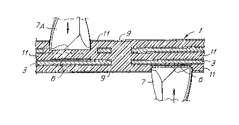
In the condition shown in Fig.7, the component CE
results to be cooled only by the transit of the heat
from its base and from the side ~alls of its lower
cylindrical portion to the metal layer 3 with which
it is in contact inside the cavity 13, this heat moving
along said la~er as far as the outside and also being
able to dissipate through the other layers of the
multilayer. However, and especially for components
whose operating functions give rise to a larger amoun-t
of heat to be cooled off, the method offers the
possibility of transferring said amoun-t of heat to an
outer dissipator member, like those indicated by 21 in
Figs.8 and 9. In the example of Figo8, the dissipator
member 21, provided with fins 23 to facilitate the air
cooling, is equippad with at least two metal rods 25
and 27 solid therewith, the one indicated by 25 bein~
inserted and welded in a metallized cavity 29 similar
to the cavity 13 and likewise formed, while the rod 27
is inserted and welded in a metallized through~hole 31;
both the cavity 29 and the hole 31 being connected, for
heat transfer purposes, with the inner layer 3 which
receives heat from the component ~E~ ~he cavity like
that indicated by 29 and the holes like that indicated
b~ 31 are suitably located around -the component or
around groups o~ components~ In the example of Fig.9,
-- 8 --
: .. : , .~ : ,
the dissipator member 21 results connected wi-th the
inner layer 3 - which receives heat - through at
least -two rods 25' and 27' both welded insi.de the
metallized through-holes 31', this solution being
preferable as the layer 3 is located further in depth,
that is, more spaced than in the case shown in Fig.8,
in respect to the face of the multilayer on which -the
component is applied. Whereas Fig.8 shows an example of
mixed ( 90 to speak) connection of the element 21 with
the layer 3, that is a connection performed in two
different ways, in -the example of ~ig.10, the rods 25
and 27 are both welded inside cavities 29.
It should be noted that the layer 3 is usually a
layer having the function to "ground" connect the individual
components, which are then connected - according to the
circuit diagram, by means of weldings 35 - o~ the portions
19 of the circuit which is printed, that is,photo-engraved
on the multilayer after the described metallization step.
The dissipator members 21 may be also cooled through
forced ventilation; moreover, they may be variously
shaped as show.n in the examples of ~ig.11 wherein 21C
i.ndicates a plan view of an element being rectangular
on top~ while 21Q indicates a similar view of a square
shaped element made up by the union of four straight
elements and which has four rods 23 to receive the heat
_ 9 _
~ ~;i3~
from the layer 3 being in contact with the component
base.
The method provides also for -the utilization of
external heat dissipato.rs of tubular (or similar)
type, internally cooled by water or other cooling
fluid~ In Fi~.12, a mul-tilayer 1, with a cavity 1~
for a parallelepiped component CE, drawn with dotted
linesg results cooled by the cooling liquid circulating
in the -tubing 39O The tubing 39 is supported by and
receives the heat from blocks 41 which are provided
with lower shanks 43 inser-ted into metallized through-
-holes 31 o~ the multilayer, said shanks receiving the
heat from the metal layer 3 on which the component CE
restsO The heat dissipator, made up of the two right-angle
branches of the tubing 39, is substantially similar to
that9 made up of a U-shaped tubing ~5 borne by blocks
51, shown in plan view on the right in ~ig.11.
The heat dissipation system which results from the
in~ention method is particularly advantageous when
multilayers having high dimensional stability like -those
hereinbefore described are used, in case of possible
overhea-ting o~ the components during their "switch-on/
/swi-tch-o~f" operation since, in this case, the components
thermally expand in a different wa~ -from the base support
thereo-f, -that is from the multilayer. Upon the "swi-tch-on/
10 -
.~
,
3~
/switch-off" operation, a breaking of the so-called
"leadless" (tha-t iS9 without an inteI~ediate lead)
weldings of the components may often occur owing to
the above said differences in thermal expansion; a
good heat dissipation represents, in -this case, a
radical solution of the problem.
The method o-f the invention can be obvlously applied
also -to multilayers laminates less valuable, so to
speak, than those having high dimensional stability as
mentioned in this description, that is, multilayers
with at least one metal layer disposed inside the
insulating layers, all without particular characteristics
of non-de-formability~ However, in case of multilayers
o~ the type taken into consideration, the method is capa=
ble of advantageously integrating their ~haracteristics by
broadening the possibilities of use thereof~
It is understood that the drawing shows an exemplification
given only as a practical demonstratlon of the inven-tion,
as this may vary in the forms and dispositions without
nevertheless departing from the scope of the idea on
which the same invention is based.
;
. .
.. . : .